PERIPHERAL PROGRAMMABLE-LOGIC DEVICES
A programmable peripheral device is designed to perform various interface functions. Such a device can be set up to perform specific functions by writing an instruction (or instructions) in its internal register, called the control register. This function can be changed during execution by writing a new instruction in this register. These devices are flexible, versatile, and economical; they are widely used in microprocessor-based products.
A programmable device, on the other hand, has its functions determined through software instructions. A programmable peripheral device can not only be viewed as a multiple I/O device, but it also performs many other functions, such as time delay, interrupt handling, and graphic user machine interactions, etc. In fact, it consists of many devices on a single chip, interconnected through a common bus. This is a hardware approach through software control to performing the I/O functions, discussed earlier in this chapter.
This section describes five typical programmable peripheral devices: programmable I/O ports; interrupt controller; timer; CMOS (complementary metal-oxide-semiconductor); and DMA (direct memory access).
Programmable peripheral I/O ports
The programmable peripheral interface, especially the 8255 programmable peripheral I/O interface, is a very popular and versatile input and output chip, easily configured to function in several different configurations. The 8255 is used on several ranges of interface cards that plug into an available slot in controllers or computers, allowing the use of both digital input and output.
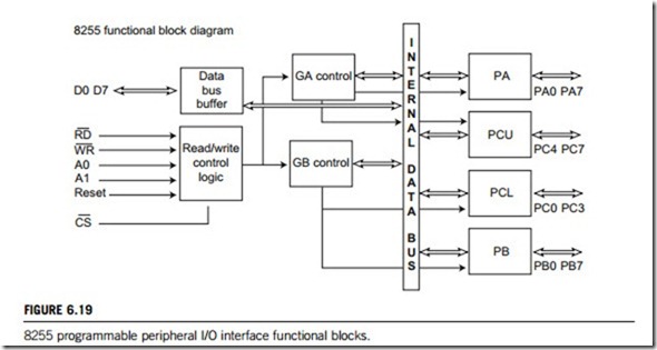
As illustrated in Figure 6.19, each 8255 programmable peripheral I/O interface has three 8-bit TTL-compatible I/O ports that will allow the control of up to 24 individual outputs or inputs. For example, they can be attached to a robotic device to control movement by use of motors to control motion and switches to detect position, etc.
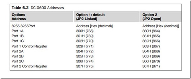
Addressing ports is different from addressing memory, as ports have port addresses and memory has memory addresses; port address 1234 is different from memory address 1234. The 8255 programmable peripheral I/O interface cards use port addresses and cannot be set to use memory addresses (see Table 6.2). They plug into any available 8- or 16-bit slot (also known as an AT or ISA slot) on the motherboard of a controller in the same way a sound card or disk drive controller card. The CPU of the motherboard communicates with the cards via its address. By physically using jumpers on the card, we can assign a set of addresses to the card; then in software, we can tell the CPU what these addresses are (more discussion about this are in the FPGA subsection on programming).
Before the chip can be used, its configuration must be set. This tells the 8255 whether ports are input, output or some strange arrangements called bidirectional and strobed. The 8255 allows for three distinct operating modes (modes 0, 1, and 2) as follows:
1. Mode 0: basic input/output. Ports A and B operate as either inputs or outputs and Port C is divided into two 4-bit groups either of which can be operated as inputs or outputs.
2. Mode 1: strobed input/output. Same as Mode 0 but Port C is used for handshaking and control.
3. Mode 2: bidirectional bus. Port A is bidirectional (both input and output) and Port C is used for handshaking. Port B is not used.
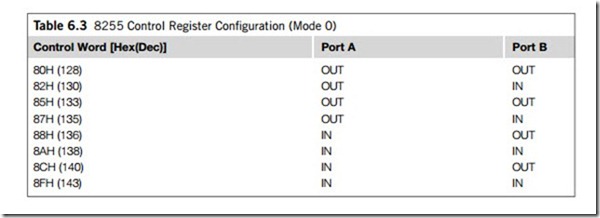
Mode 0 is the most used. Each of the three ports has 8 bits, and each of these bits can be indi- vidually set ON or OFF, somewhat like having three banks of eight light switches. These bits are configured, in groups, to be inputs or outputs. The various modes can be set by sending a value to the control port. The control port is Base Address þ 3 (i.e., 768 þ 3 ¼ 771 decimal). Table 6.3 shows the different arrangements that can be configured and the values to be sent to the configu- ration port.
As mentioned, the control port is Base Address þ 3. Port A is always at Base Address; Port B is Base Address þ 1; Port C is Base Address þ 2. Thus, in our example Ports A, B, and C are at 768, 769, and 770 (decimal), respectively. By writing, say, 128, the control port will then configure the 8255 to have all three ports set for output.
Programmable interrupt controller chipset
Both microcontroller and microcomputer system designs require that I/O devices such as keyboards, displays, sensors, and other components receive servicing in an efficient manner so that most of the total system tasks can be assumed by the microcomputer with little or no effect on throughput. As mentioned in subsection 5.1.2, there are two common methods of servicing such devices the polled approach and the interrupt method, which allows the microprocessor to continue executing its main program and only stop to service peripheral devices when told to do so by the device itself.
The programmable interrupt controller (PIC) functions as an overall manager in an interrupt-driven system environment. It accepts requests from the peripheral equipment, determines which of the incoming requests is of the highest importance (priority), ascertains whether the incoming request has a higher priority value than the level currently being serviced, and issues an interrupt to the CPU based on this determination. The PIC, after issuing an interrupt to the CPU, must input information into the CPU that can “point” the program counter to the correct service routine. This “pointer” is an address in a vectoring table, and will be referred to, in this document, as vectoring data.
The 8259A is taken as an example of the PIC. It manages eight levels of requests and has built-in
features for expandability to other 8259As (up to 64 levels). It is programmed by the system’s software as an I/O peripheral. A selection of priority modes is available to the programmer so that the manner in which the requests are processed can be configured to match system requirements. Priority modes can be changed or reconfigured dynamically whenever the main program is executing. This means that the complete interrupt structure can be defined on the requirements of the total system environment.
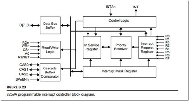
Figure 6.20 gives the block function diagram of 8259A PIC, which includes these function blocks and pins:
1. Interrupt request register (IRR) and in-service register (ISR). The interrupts at the IR input lines are handled by two registers in cascade, the IRR and the ISR. The IRR is used to store all the interrupt levels that are requesting service, and the ISR is used to store all the interrupt levels that are being serviced.
2. Priority resolver. This logic block determines the priorities of the bits set in the IRR. The highest priority is selected and strobed into the corresponding bit of the ISR during INTA pulse.
3. Interrupt mask register (IMR). The IMR stores the bits that mask the interrupt lines that are to be
masked. The IMR operates on the IRR. Masking of a higher-priority input will not affect the interrupt request lines of lower priority.
4. INT (interrupt). This output goes directly to the CPU interrupt input. The VOH level on this line is
designed to be fully compatible with the 8080A, 8085A, and 8086 input levels.
5. INTA (interrupt acknowledge). INTA pulses will cause the 8259A to release vectoring information onto the data bus. The format of these data depends on the system mode (mPM) of the 8259A.
6. Data bus buffer. This is a three-state, bidirectional 8-bit buffer that is used to interface the 8259A to
the system data bus. Control words and status information are transferred through the data bus buffer.
7. Read/write control logic. The function of this block is to accept OUTPUT commands from the
CPU. It contains the initialization command word (ICW) registers and operation command word (OCW) registers that store the various control formats for device operation. This function block also allows the status of the 8259A to be transferred onto the data bus.
244 CHAPTER 6 Programmable logic and application specific integrated circuits (PLASIC)
8. CS (chip select). A LOW on this input enables the 8259A. No reading or writing of the chip will occur unless the device is selected.
9. WR (write). A LOW on this input enables the CPU to write control words (ICWs and OCWs) to the 8259A.
10. RD (read). A LOW on this input enables the 8259A to send the status of the IRR, ISR, IMR, or the interrupt level onto the data bus.
11. A0. This input signal is used in conjunction with WR and RD signals to write commands into the
various command registers, as well as reading the various status-registers of the chip. This line can be tied directly to one of the address lines.
12. The cascade buffer/comparator. This function block stores and compares the IDs of all 8259A that
are used in the system. The associated three I/O pins (CAS0-2) are outputs when the 8259A is used as a master, and are inputs when the 8259A is used as a slave. As a master, the 8259A sends the ID of the interrupting slave device onto the CAS0 ± 2 lines. The slave thus selected will send its pre-programmed subroutine address onto the data bus during the next one or two consecutive INTA pulses.
The powerful features of the 8259A in a microcomputer system are its programmability and interrupt routine addressing capability. The latter allows direct or indirect jumping to the specific interrupt routine requested without any polling of the interrupting devices. The normal sequence of events during an interrupt depends on the type of CPU being used. The events occur as follows in an MCS-80/ 85 system:
1. One or more of the INTERRUPT REQUEST lines (IR7 ± 0) are raised high, setting the corresponding IRR bit(s).
2. The 8259A evaluates these requests and sends an INT to the CPU, if appropriate.
3. The CPU acknowledges the INT and responds with an INTA pulse.
4. Upon receiving an INTA from the CPU group, the highest-priority ISR bit is set, and the corresponding IRR bit is reset. The 8259A will also release a CALL instruction code (11001101) onto the 8-bit data bus through its D7 ± 0 pins.
5. This CALL instruction will initiate two more INTA pulses to be sent to the 8259A from the CPU group.
6. These two INTA pulses allow the 8259A to release its pre-programmed subroutine address onto the
data bus. The lower 8-bit address is released at the first INTA pulse and the higher 8-bit address is released at the second INTA pulse.
7. This completes the 3-byte CALL instruction released by the 8259A. In the AEOI mode the ISR bit
is reset at the end of the third INTA pulse. Otherwise, the ISR bit remains set until an appropriate EOI command is issued at the end of the interrupt sequence.
The events occurring in an 8086 system are the same until the fourth step; from the fourth step onward:
(d) Upon receiving an INTA from the CPU group, the highest-priority ISR bit is set and the corresponding IRR bit is reset. The 8259A does not drive the data bus during this cycle.
(e) The 8086 will initiate a second INTA pulse. During this pulse, the 8259A releases an 8-bit pointer onto the data bus where it is read by the CPU.
(f) This completes the interrupt cycle.
In the AEOI mode the ISR bit is reset at the end of the second INTA pulse. Otherwise, the ISR bit remains set until an appropriate EOI command is issued at the end of the interrupt subroutine. If no interrupt request is present at step (d) of either sequence (i.e., the request was too short in duration) the 8259A will issue an interrupt level 7. Both the vectoring bytes and the CAS lines will look as if an interrupt level 7 was requested.
When the 8259A PIC receives an interrupt, INT becomes active and an interrupt acknowledge cycle is started. If a higher-priority interrupt occurs between the two INTA pulses, the INT line goes inactive immediately after the second INTA pulse. After an unspecified amount of time the INT line is activated again to signify the higher-priority interrupt waiting for service. This inactive time is not specified and can vary between parts. The designer should be aware of this consideration when designing a system that uses the 8259A. It is recommended that proper asynchronous design techniques be followed.
Advanced programmable interrupt controllers (APICs) are designed to attempt to solve interrupt
routing efficiency issues in multiprocessor computer systems. There are two components in the Intel APIC system; the local APIC (LAPIC) and the IOAPIC. The LAPIC is integrated into each CPU in the system, and the IOAPIC is used throughout the system’s peripheral buses, typically one for each bus. In the original system designs, LAPICs and IOAPICs were connected by a dedicated APIC bus. Newer systems use the system bus for communication between all APIC components.
LAPICs manage all external interrupts for the processor that it is part of. In addition, they are able to accept and generate interprocessor interrupts (IPIs) between LAPICs. LAPICs may support up to 224 usable IRQ vectors from an IOAPIC. Vectors numbers 0 31, out of 0 255, are reserved for exception handling by x86 processors.
IOAPICs contain a redirection table, which is used to route the interrupts it receives from peripheral buses to one or more LAPICs.
Programmable timer controller chipset
The programmable timer controller provides a programmable interval timer and counter that are designed to solve one of the most common problems in any microcomputer system; the generation of accurate time delays by software control. Instead of setting up timing loops in software, the programmer configures the programmable timer controller to the desired delay. After this time, the programmable timer controller will interrupt the CPU. Software overhead is minimal and variable- length delays can easily be accommodated.
Some of the other computer and timer functions that it can implement are real-time clock, event counter, digital one-shot, programmable rate generator, square-wave generator, binary rate multiplier, complex waveform generator, and complex motor controller.
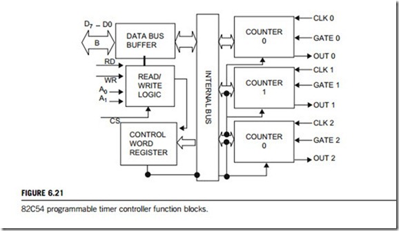
Figure 6.21 gives the typical function blocks for an 82C54 programmable interval timer controller, which has these main blocks:
1. Data bus buffer. This three-state, bidirectional 8-bit buffer is used to interface the 82C54 to the system bus.
2. Read/write logic. The read/write logic accepts inputs from the system bus and generates control
signals for the other functional blocks of the 82C54. A1 and A0 select one of the three counters on the control word register to be read from or written into. A “low” on the RD input tells the 82C54 that the CPU is reading one of the counters. A “low” on the WR input tells the 82C54 that the CPU is writing either a control word or an initial count. Both RD and WR are qualified by CS; RD and WR are ignored unless the 82C54 has been selected by holding CS low.
3. Control word register. The control word register is selected by the read/write logic when A1, A0 ¼
11. If the CPU then does a write operation to the 82C54, the data are stored in the control word
register and interpreted as a control word used to define the counter operation. The control word register can only be written to.
4. Counter 0, Counter 1, Counter 2. These three functional blocks are identical in operation, so only
a single counter will be described. The counters are fully independent. Each counter may operate in a different mode.
The programmable timer is normally treated by the system software as an array of peripheral I/O ports; three are counters and the fourth is a control register for mode programming. Basically, the select inputs A0, A1 connects to the A0, A1 address bus signals of the CPU. The CS can be derived directly from the address bus by using a linear select method, or it can be connected to the output of a decoder.
After power-up, the state of the programmable timer is undefined, as are the mode, count value, and output of all counters. Each counter operates a determined when programmed which must happen before use. Unused counters need not be programmed. They are programmed by writing a control word and then an initial count. All control words are written into the control word register, which is selected when A1, A0 ¼ 11. The control word specifies which counter is being programmed. By contrast, initial counts are written into the counters, not the control word register. The A1, A0 inputs are used to select the counter to be written into. The format of the initial count is determined by the control word used.
1. Write operations. A new initial count may be written to a counter at any time without affecting the counter’s programmed mode in any way. Counting will be affected as described in the mode definitions.
The new count must follow the programmed count format. If a counter is programmed to read and write 2-byte counts, the following precaution applies. A program must not transfer control between writing the first and second byte to another routine that also writes into that same counter. Otherwise, the counter will be loaded with an incorrect count.
2. Read operations. There are three possible methods for reading the counters. The first is through the read-back command. The second is a simple read operation of the counter, which is selected with the A1, A0 inputs. The only requirement is that the CLK input of the selected counter must be inhibited by using either the GATE input or external logic. Otherwise, the count may be in the process of changing when it is read, giving an undefined result.
CMOS chipset
The complementary metal-oxide-semiconductor (CMOS) chip is battery-powered and stores the hard drive’s configuration and other information. In a microcomputer and a microcontroller, CMOS chips normally provide real-time clock (RTC) and CMOS memory.
The real-time clock provides the board with a time-of-day clock, periodic interrupt, and system configuration information. In personal computers, the CMOS chipset typically contains 64 (00hex- 3Fhex) 8-bit locations of battery-backed-up CMOS RAM (random access memory). The split is (1) 00hex 0Ehex, used for real-time clock functions (time of day), (2) 0Fhex 35hex, used for system configuration information, for example, hard drive type, memory size, etc., and (3) 36hex 3Fhex, used for power-on password storage.
CMOS memory is an accessible set of memory locations on the same chip as the RTC and has its own battery backup so that it retains both functions, even when the computer is turned off. Battery-powered CMOS and RTCs did not exist in early systems and the current time was entered manually every time the system was turned on. This memory location in CMOS is separate from the RTC registers and is generally updated by the BIOS which can update the century information, as can many operating systems, network time systems, and applications, or the user can set it using the right commands.
Direct memory access controller chipset
Direct memory access (DMA) is an I/O technique commonly used for high-speed data transfer among internal memories, I/O ports, and peripherals, and also between the memories and I/O devices on different chipsets. The DMA technique allows the microprocessor to release bus control to a device called a DMA controller. The DMA controller manages data transfer between memory and a periph- eral under its control, thus bypassing the microprocessor. The microprocessor communicates with the controller by using the chip select line, buses, and control signals. However, once the controller has gained control, it plays the role of a microprocessor for data transfer. For all practical purposes, the DMA controller is a microprocessor capable only of copying data at high speed from one location to another. An illustration of a programmable DMA controller, the Intel 8237A, is described below.
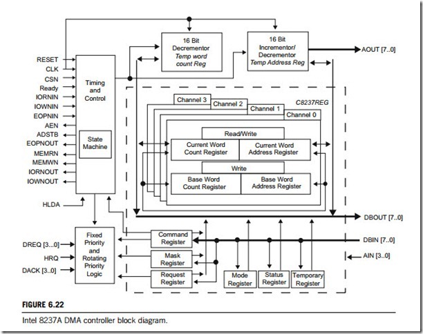
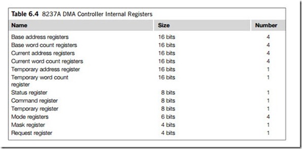
The 8237A block diagram shown in Figure 6.22 includes its major logic blocks and all the internal registers. The data interconnection paths are also shown. Not shown are the various control signals between the blocks. The 8237A contains 344 bits of internal memory in the form of registers. Table 6.4 lists these registers by name and shows the size of each. It contains three basic blocks of control logic; the timing control block generates internal timing and external control signals for the 8237A. The program command control block decodes the various commands given to the 8237A by the micro- processor prior to servicing a DMA request, and also decodes the mode control word used to select the type of DMA during the servicing. The priority encoder block resolves priority contention between DMA channels that are requesting service simultaneously.
To perform block moves of data from one memory address space to another with a minimum of program effort and time, the 8237A includes a memory-to-memory transfer feature. Programming a bit in the command register selects channels 0 and 1 to operate as memory-to-memory transfer channels. The transfer is initiated by setting the software DREQ for channel 0. The 8237A requests a DMA service in the normal manner. After HLDA is true, the device, using four-state transfers in block transfer mode, reads data from the memory. The channel 0 current address register is the source for the address used and is decremented or incremented in the normal manner. The data byte read from the memory is stored in the 8237A internal temporary register. Channel 1 then performs a four-state transfer of the data from the temporary register to memory using the address in its current address register and incrementing or decrementing it in the normal manner. The channel 1 current word count is decremented. When the word count of channel 1 goes to FFFFH, a TC is generated causing an EOP output terminating the service. Channel 0 may be programmed to retain the same address for all transfers. This allows a single word to be written to a block of memory. The 8237A will respond to external EOP signals during memory-to-memory transfers. Data comparators in block search schemes may use this input to terminate the service when a match is found.
The 8237A will accept programming from the host processor at any time that the HLDA is inactive; this is true even if HRQ is active. The responsibility of the host is to ensure that programming and HLDA are mutually exclusive. Note that a problem can occur if a DMA request occurs on an unmasked channel while the 8237A is being programmed. For instance, the CPU may be starting to reprogram the 2-byte address register of channel 1 when channel 1 receives a DMA request. If the 8237A is
enabled (bit 2 in the command register is 0) and channel 1 is unmasked, a DMA service will occur after only 1 byte of the address register has been reprogrammed. This can be avoided by disabling the controller (setting bit 2 in the command register) or masking the channel before programming any other registers. Once the programming is complete, the controller can be enabled and unmasked. After power-up it is suggested that all internal locations, especially the mode register, be loaded with some valid value. This should be done even if some channels are unused. An invalid mode may force all control signals to go active at the same time.
The 8237A is designed to operate in two major cycles. These are called idle and active cycles. Each device cycle is made up of a number of states. The 8237A can assume seven separate states, each composed of one full clock period. State I (SI) is the inactive state. It is entered when the 8237A has no valid DMA requests pending. While in SI, the DMA controller is inactive but may be in program condition, being programmed by the processor. State S0 (S0) is the first state of a DMA service. The 8237A has requested a hold but the processor has not yet returned an acknowledgement. The 8237A may still be programmed until it receives HLDA from the CPU. An acknowledgement from the CPU
will signal that DMA transfers may begin. S1, S2, S3, and S4 are the working states of the DMA service. If more time is needed to complete a transfer than is available with normal timing, wait states (SW) can be inserted between S2 or S3 and S4 by the use of the ready line on the 8237A. Eight states are required for a single transfer. The first four states (S11, S12, S13, S14) are used for the read-from- memory half and the last four states (S21, S22, S23, S24) for the write-to-memory half of the transfer.
(1) Idle cycle
When no channel is requesting service, the 8237A will enter the idle cycle and perform “SI” states. In this cycle the 8237A will sample the DREQ lines every clock cycle to determine whether any channel is requesting a DMA service. The device will also sample CS, looking for an attempt by the microprocessor to write or read the internal registers of the 8237A. When CS is low and HLDA is low, the 8237A enters the program condition. The CPU can now establish, change, or inspect the internal definition of the part by reading from or writing to the internal registers. Address lines A0 ± A3 are inputs to the device and select which registers will be read or written. The IOR and IOW lines are used to select and time reads or writes. Special software commands can be executed by the 8237A in the program condition. These commands are decoded as sets of addresses with the CS and IOW. The commands do not make use of the data bus. Instructions include Clear First/Last Flip-Flop and Master Clear.
(2) Active cycle
When the 8237A is in the idle cycle and a nonmasked channel requests a DMA service, the device will output an HRQ to the microprocessor and enter the active cycle. It is in this cycle that the DMA service will take place, in one of four modes:
1. Single transfer mode. In single transfer mode the device is programmed to make one transfer only.
The word count will be decremented, and the address decremented or incremented following each transfer. When the word count rolls over from 0 to FFFFH, a terminal count (TC) will cause an auto-initialize if the channel has been programmed to do so. DREQ must be held active until DACK becomes active in order to be recognized. If DREQ is held active throughout the single transfer, HRQ will go inactive and release the bus to the system. It will again go active and, upon receipt of a new HLDA, another single transfer will be performed. Details of timing between the 8237A and other bus control protocols will depend upon the characteristics of the microprocessor involved.
2. Block transfer mode. In block transfer mode the device is activated by DREQ to continue making transfers during the service until a TC, caused by word count going to FFFFH, or an external end- of-process (EOP) is encountered. DREQ need only be held active until DACK becomes active. Again, an auto-initialization will occur at the end of the service if the channel has been programmed for it.
3. Demand transfer mode. In demand transfer mode the device is programmed to continue making transfers until a TC or external EOP is encountered or until DREQ goes inactive. Thus, transfers may continue until the I/O device has exhausted its data capacity. After the I/O device has had a chance to catch up, the DMA service is re-established by means of a DREQ. During the time between services when the microprocessor is allowed to operate, the intermediate values of address and word count are stored in the 8237A current address and current word count registers. Only an EOP can cause an auto-initialize at the end of the service. EOP is generated either by TC or by an external signal. DREQ has to be low before S4 to prevent another transfer.
4. Cascade mode. This mode is used to cascade more than one 8237A together for simple system expansion. The HRQ and HLDA signals from the additional 8237A are connected to the DREQ and DACK signals of a channel of the initial 8237A. This allows the DMA requests of the additional device to propagate through the priority network circuitry of the preceding device. The priority chain is preserved and the new device must wait for its turn to acknowledge requests. Since the cascade channel of the initial 8237A is used only for prioritizing the additional device, it does not output any address or control signals of its own. These could conflict with the outputs of the active channel in the added device. The 8237A will respond to DREQ and DACK but all other outputs except HRQ will be disabled. The ready input is ignored.
Each of the three active transfer modes above can perform three different types of transfers; read, write, and verify. Write transfers move data from an I/O device to the memory by activating MEMW and IOR. Read transfers move data from memory to an I/O device by activating MEMR and IOW. Verify transfers are pseudotransfers. The 8237A operates as in read or write transfers generating addresses, and responding to EOP, etc. However, the memory and I/O control lines all remain inactive. The ready input is ignored in verify mode.
