Constant-Current Sources and “Current Mirrors”
As mentioned earlier, the use of high-value collector load resistors in the interests of high stage gain and low inherent distortion carries with it the penalty that the performance of the amplifying device may be impaired by the low collector current levels that result from this approach.
Advantage can, however, be taken of the very high output impedance of a junction transistor, which is inherent in the type of collector current/supply voltage characteristics
illustrated in Figure 7.21, where even at currents in the 1- to 10-mA region, dynamic impedances of the order of 100 kilohms may be expected.
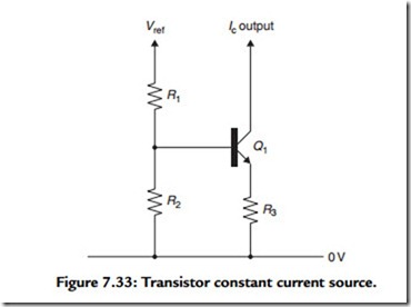
A typical circuit layout that utilizes this characteristic is shown in Figure 7.33, in which R1 and R2 form a potential divider to define the base potential of Q1, and R3 defines the total emitter or collector currents for this effective base potential.
This configuration can be employed with transistors of either PNP or NPN types, which allow the circuit designer considerable freedom in their application.
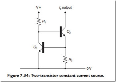
An improved, two-transistor, constant current source is shown in Figure 7.34. In this, R1 is used to bias Q2 into conduction, and Q1 is employed to sense the voltage developed across R2, which is proportional to emitter current, and to withdraw the forward bias from Q2 when that current level is reached at which the potential developed across R2 is just sufficient to cause Q1 to conduct.
The performance of this circuit is greatly superior to that of Figure 7.33 in that the output impedance is about 10x greater and the circuit is insensitive to the potential, +Vref., applied to R1, so long as it is adequate to force both Q2 and Q1 into conduction.
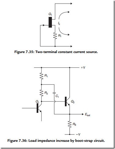
An even simpler circuit configuration makes use of the inherent very high output impedance of a junction FET under constant gate bias conditions. This employs the circuit layout shown in Figure 7.35, which allows a true “two-terminal” constant current
source, independent of supply lines or reference potentials, and which can be used at either end of the load chain.
The current output from this type of circuit is controlled by the value chosen for R1, and this type of constant current source may be constructed using almost any available junction FET, provided that the voltage drop across the FET drain-gate junction does not exceed the breakdown voltage of the device. This type of constant current source is also available as small, plastic-encapsulated, two-lead devices, at a relatively low cost, and with a range of specified output currents.
All of these constant current circuit layouts share the common small disadvantage that they will not perform very well at low voltages across the current source element. In the case of Figures 7.33 and 7.34, the lowest practicable operating potential will be about 1 V. The circuit of Figure 7.35 may require, perhaps, 2–3 V, and this factor must be considered in circuit performance calculations.
The “boot-strapped” load resistor arrangement shown in Figure 7.36, and commonly used in earlier designs of audio amplifier to improve the linearity of the last class ‘A’ amplifier stage (Q1), effectively multiplies the resistance value of R2 by the gain which Q2 would be deemed to have if operated as a common-emitter amplifier with a collector load of R3 in parallel with R1.
This arrangement is the best configuration practicable in terms of available rms output voltage swing as compared with conventional constant current sources, but has fallen into
disuse because it leads to slightly lower quality THD figures than are possible with other circuit arrangements.
All these circuit arrangements suffer from a further disadvantage, from the point of view of the integrated circuit designer: they employ resistors as part of the circuit design, and resistors, although possible to fabricate in IC structures, occupy a disproportionately large area of the chip surface. Also, they are difficult to fabricate to precise resistance values without resorting to subsequent laser trimming, which is expensive and time-consuming.
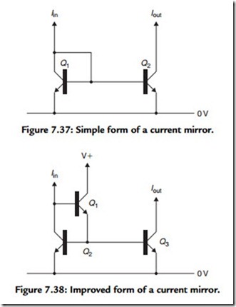
Because of this, there is a marked preference on the part of IC design engineers for the use of circuit layouts known as “current mirrors,” of which a simple form is shown in Figure 7.37.
7.14.1 IC Solutions
These are not true constant current sources in that they are only capable of generating an output current (Lout) that is a close equivalent of the input or drive current (Lin). However, the output impedance is very high, and if the drive current is held to a constant value, the output current will also remain constant.
A frequently found elaboration of this circuit, which offers improvements in respect to output impedance and the closeness of equivalence of the drive and output currents, is shown in Figure 7.38. Like the junction FET-based constant current source, these current mirror devices are available as discrete, plastic-encapsulated, three-lead components,
having various drive current/output current ratios, for incorporation into discrete component circuit designs.
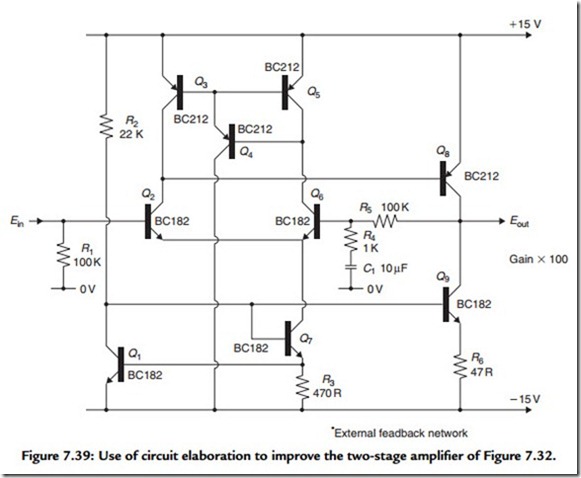
The simple amplifier circuit of Figure 7.32 can be elaborated, as shown in Figure 7.39, to employ these additional circuit refinements, which would have the effect of increasing the open-loop gain, that is, that before negative feedback is applied, by 10-100x and improving the harmonic and other distortions, and the effective bandwidth by perhaps 3-10x . From the point of view of the IC designer, there is also the advantage of a potential reduction in the total resistor count.
These techniques for improving the performance of semiconductor amplifier stages find particular application in the case of circuit layouts employing junction FETs and
MOSFETs, where the lower effective mutual conductance values for the devices would normally result in relatively poor stage gain figures.
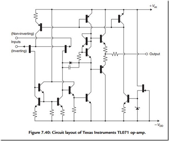
This has allowed the design of IC operational amplifiers, such as the RCA CA3140 series or the Texas Instruments TL071 series, which employ, respectively, MOSFET and junction FET input devices. The circuit layout employed in the TL071 is shown, by way of example, in Figure 7.40.
Both of these op-amp designs offer input impedances in the million megohm range— in comparison with the input impedance figures of 5–10 kilohm, which were typical of early bipolar ICs—and the fact that the input impedance is so high allows the use of such ICs in circuit configurations for which earlier op-amp ICs were entirely inappropriate.
Although the RCA design employs MOSFET input devices, which offer, in principle, an input impedance that is perhaps 1000 times better than this figure, the presence of on-chip Zener diodes, to protect the device against damage through misuse or static electric charges, reduces the input impedance to roughly the same level as that of the junction FET device.
It is a matter for some regret that the design of the CA3140 series devices is now so elderly that the internal MOSFET devices do not offer the low level of internal noise of which more modern MOSFET types are capable. This tends to rule out the use of this MOSFET op-amp for high-quality audio use, although the TL071 and its equivalents, such as the LF351, have demonstrated impeccable audio behavior.
