Audibility of Distortion
Harmonic and Intermodulation Distortion
Because of the small dissipations that are normally involved, almost all discrete component voltage amplifier circuitry will operate in class ‘A’ (that condition in which the bias applied to the amplifying device is such as to make it operate in the middle of the linear region of its input/output transfer characteristic), and the residual harmonic components are likely to be mainly either second or third order, which are audibly much more tolerable than higher order distortion components.
Experiments in the late 1940s suggested that the level of audibility for second and third harmonics was of the order of 0.6 and 0.25%, respectively, which led to the setting of a target value, within the audio spectrum, of 0.1% THD, as desirable for high-quality audio equipment.
However, recent work aimed at discovering the ability of an average listener to detect the presence of low-order (i.e., second or third) harmonic distortions has drawn the uncomfortable conclusion that listeners, taken from a cross section of the public, may rate a signal to which 0.5% second harmonic distortion has been added as “more musical” than, and therefore preferable to, the original undistorted input. This discovery tends to cast doubt on the value of some subjective testing of equipment.
What is not in dispute is that the intermodulation distortion (IMD), which is associated with any nonlinearity in the transfer characteristics, leads to a muddling of the sound picture so that if the listener is asked not which sound he prefers, but which sound seems to him to be the clearer, he will generally choose that with the lower harmonic content.
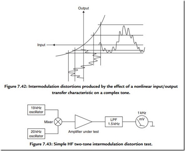
The way in which IMD arises is shown in Figure 7.42, where a composite signal containing both high-frequency and low-frequency components, fed through a nonlinear
system, causes each signal to be modulated by the other. This is conspicuous in the drawing in respect to the HF component, but is also true for the LF one.
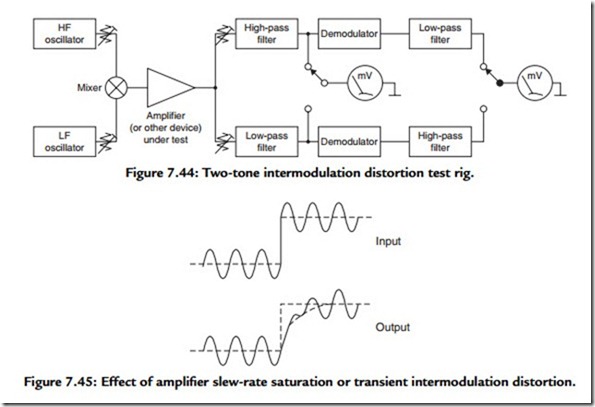
This can be shown mathematically to be due to the generation of sum and difference products, in addition to the original signal components, and provides a simple method, shown schematically in Figure 7.43, for the detection of this type of defect. A more formal IMD measurement system is shown in Figure 7.44.
With present circuit technology and device types, it is customary to design for total harmonic and IM distortions to be below 0.01% over the range 30 Hz–20 kHz, and at all signal levels below the onset of clipping. Linear IC op-amps, such as the TL071 and the LF351, will also meet this specification over the frequency range 30 Hz–10 kHz.
Transient Defects
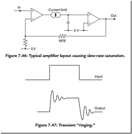
A more insidious group of signal distortions may occur when brief signals of a transient nature, or sudden step type changes in base level, are superimposed on the more continuous components of the program signal. These defects can take the form of slew-rate distortions, usually associated with a loss of signal during the period of the slew-rate saturation of the amplifier—often referred to as transient intermodulation distortion or TID.
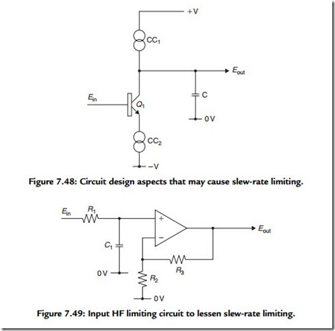
This defect is illustrated in Figure 7.45 and arises particularly in amplifier systems employing substantial amounts of negative feedback when there is some slew-rate limiting component within the amplifier, as shown in Figure 7.46.
A further problem is that due to “overshoot,” or “ringing,” on a transient input, as illustrated in Figure 7.47. This arises particularly in feedback amplifiers if there is an inadequate stability margin in the feedback loop, particularly under reactive load
conditions, but will also occur in low-pass filter systems if too high an attenuation rate is employed.
The ear is very sensitive to slew-rate induced distortion, which is perceived as a “tizziness” in the reproduced sound. Transient overshoot is normally noted as a somewhat overbright quality. The avoidance of both these problems demands care in the circuit design, particularly when a constant current source is used, as shown in Figure 7.48.
In this circuit, the constant current source, CC1, will impose an absolute limit on the possible rate of change of potential across the capacitance, C1 (which could well be simply the circuit stray capacitance), when the output voltage is caused to move in a positive-going direction. This problem is compounded if an additional current limit mechanism, CC2, is included in the circuitry to protect the amplifier transistor (Q1) from output current overload.
Since output load and other inadvertent capacitances are unavoidable, it is essential to ensure that all such current limited stages operate at a current level that allows potential slewing to occur at rates that are at least 10x greater than the fastest signal components. Alternatively, means may be taken, by way of a simple input integrating circuit, (R1C1), as shown in Figure 7.49, to ensure that the maximum rate of change of the input signal voltage is within the ability of the amplifier to handle it.
Spurious Signals
In addition to harmonic, IM, and transient defects in the signal channel, which will show up on normal instrumental testing, there is a whole range of spurious signals that may not arise in such tests. The most common of these is that of the intrusion of noise and alien signals, either from the supply line or by direct radio pick up.
This latter case is a random and capricious problem that can only be solved by steps appropriate to the circuit design in question. However, supply line intrusions, whether because of unwanted signals from the power supply or from the other channel in a stereo system, may be reduced greatly by the use of circuit designs offering a high immunity to voltage fluctuations on the DC supply.
Other steps, such as the use of electronically stabilized DC supplies or the use of separate power supplies in a stereo amplifier, are helpful, but the required high level of supply line signal rejection should be sought as a design feature before other palliatives are applied. Modern IC op-amps offer a typical supply voltage rejection ratio of 90 dB (30,000:1). Good discrete component designs should offer at least 80 dB (10,000:1).
This figure tends to degrade at higher frequencies, which has led to the growing use of supply line bypass capacitors having a low effective series resistance. This feature is either a result of the capacitor design or is achieved in the circuit by the designer’s adoption of groups of parallel connected capacitors chosen so that the AC impedance remains low over a wide range of frequencies.
A particular problem in respect to spurious signals, which occurs in audio power amplifiers, is a consequence of the loudspeaker acting as a voltage generator, when stimulated by pressure waves within the cabinet, and injecting unwanted audio components directly into the negative feedback loop of the amplifier. This specific problem is unlikely to arise in small signal circuitry, but the designer must consider what effect output/line load characteristics may have, particularly in respect to reduced stability margin in a feedback amplifier.
In all amplifier systems there is a likelihood of microphonic effects due to vibration of the components. This is likely to be of increasing importance at the input of “low-level,” high-sensitivity preamplifier stages and can lead to coloration of the signal when the equipment is in use, which is overlooked in the laboratory in a quiet environment.
Mains-Borne Interference
Mains-borne interference, as evidenced by noise pulses on switching electrical loads, is most commonly due to radio pick up problems and is soluble by the techniques (attention to signal and earth line paths, avoidance of excessive HF bandwidth at the input stages) that are applicable to these.


