Voltage Amplifier Design
The sources of nonlinearity in bipolar junction transistors have already been referred to, in respect to the influence of collector load impedance, and push–pull symmetry in reducing harmonic distortion. An additional factor with bipolar junction devices is the external impedance in the base circuit, as the principal nonlinearity in a bipolar device is that due to its input voltage/output current characteristics. If the device is driven from a high impedance source, its linearity will be substantially greater, since it is operating under conditions of current drive.
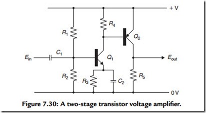
This leads to the good relative performance of the simple, two-stage, bipolar transistor circuit of Figure 7.30 in that the input transistor, Q1, is only required to deliver a very small voltage drive signal to the base of Q2 so that the signal distortion due to Q1 will
be low. Q2, however, which is required to develop a much larger output voltage swing, with a much greater potential signal nonlinearity, is driven from a relatively high source impedance, composed of the output impedance of Q1, which is very high indeed, in parallel with the base-emitter resistor, R4. R1, R2, and R3/C2 are employed to stabilize the DC working conditions of the circuit.
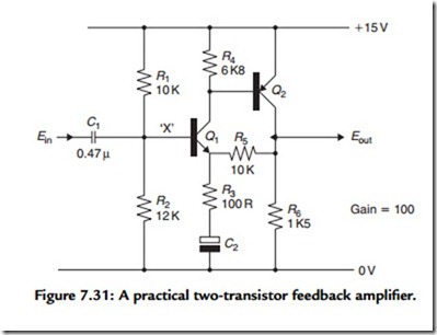
Normally, this circuit is elaborated somewhat to include both DC and AC negative feedback from the collector of Q2 to the emitter of Q1, as shown in the practical amplifier circuit of Figure 7.31.
This is capable of delivering a 14-V p-p output swing, at a gain of 100, and a bandwidth of 15 Hz to 250 kHz, at -3-dB points; largely determined by the value of C2 and the output capacitances, with a THD figure of better that 0.01% at 1 kHz.
The practical drawbacks of this circuit relate to the relatively low value necessary for R3—with the consequent large value necessary for C2 if a good LF response is desired, and the DC offset between point ‘X’ and the output, due to the base-emitter junction potential of Q1, and the DC voltage drop along R5, which makes this circuit relatively unsuitable in DC amplifier applications.
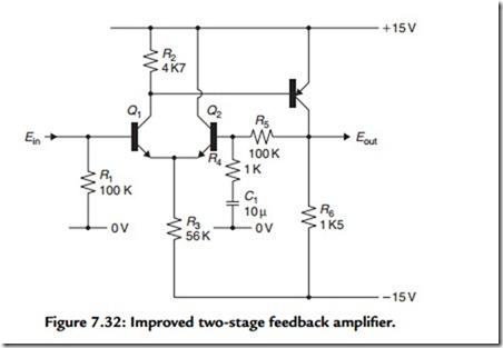
An improved version of this simple two-stage amplifier circuit is shown in Figure 7.32, in which the single input transistor has been replaced by a “long-tailed pair” configuration
of the type shown in Figure 7.32. In this, if the two-input transistors are reasonably well matched in current gain and if the value of R3 is chosen to give an equal collector current flow through both Q1 and Q2, the DC offset between input and output will be negligible, which will allow the circuit to be operated between symmetrical (+ and -) supply rails over a frequency range extending from DC to 250 kHz or more.
Because of the improved rejection of odd harmonic distortion inherent in the input “push–pull” layout, the THD due to this circuit, particularly at less than maximum output voltage swing, can be extremely low, which probably forms the basis of the bulk of linear amplifier designs. However, further technical improvements are possible, which are discussed next.


