Voltage multipliers
In all previous cases, the DC voltage is limited to the peak value of the input sine wave. When higher DC voltages are required, a step-up transformer is used. However, higher DC voltages can be produced with- out a step-up transformer. Circuits that are capable of producing higher DC voltages without the benefit of a transformer are called voltage multipliers. Two voltage multipliers are the voltage doubler and the voltage tripler.
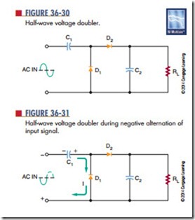
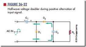
Figure 36-30 shows a half-wave voltage doubler. It produces a DC output voltage that is twice the peak value of the input signal. Figure 36-31 shows the circuit during the negative alternation of the input signal. Diode D1 conducts, and the current flows along the path shown. Capacitor C1 charges to the peak value of the input signal. Because there is no discharge path, capacitor C1 remains charged. Figure 36-32 shows the positive alternation of the input signal. At this point, capacitor C1 is charged to the negative peak value. This keeps diode D1 reverse biased and makes diode D2 for- ward biased. This allows diode D2 to conduct, charging capacitor C2. Because capacitor C1 is charged to the maximum negative value, capacitor C2 charges to twice the peak value of the input signal.
As the sine wave changes from the positive half cycle to the negative half cycle, diode D2 is cut off because capacitor C2 holds diode D2 reverse biased. Capacitor C2 discharges through the load, holding the voltage across the load constant. Therefore, it also acts as a filter capacitor. Capacitor C2 recharges only during the positive cycle of the input signal, resulting in a ripple frequency of 60 hertz (hence the name “half-wave voltage doubler”). One disadvantage of the half-wave voltage doubler is that it is difficult to filter because of the 60-hertz ripple frequency. Another disadvantage is that capacitor C2 must have a voltage rating of at least twice the peak value of the AC input signal.
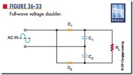
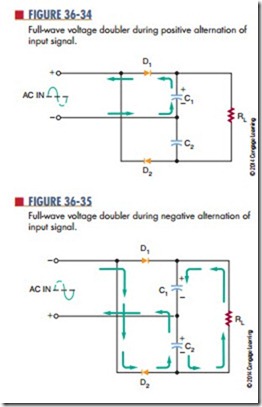
A full-wave voltage doubler overcomes some of the disadvantages of the half-wave voltage doubler. Figure 36-33 is a schematic of a circuit that operates as a full-wave voltage doubler. Figure 36-34 shows that, on the positive alternation of the input signal, capacitor C1 charges through diode D1 to the peak value of the AC input signal. Figure 36-35 shows that on the negative alternation, capacitor C2 charges through diode D2 to the peak value of the input signal.
the total voltage across the load is two times the peak value of the input signal.
Capacitors C1 and C2 are charged during the peaks of the input signal. The ripple frequency is 120 hertz because both capacitors C1 and C2 are charged during each cycle. Capacitors C1 and C1 split the output voltage to the load, so each capacitor is subject to the peak value of the input signal.
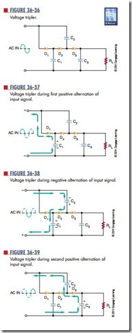
Figure 36-36 shows the circuit of a voltage tripler. In Figure 36-37, the positive alternation of the input signal
biases diode D1 so that it conducts. This charges capacitor C1 to the peak value of the input signal. Capacitor C1 places a positive potential across diode D2.
Figure 36-38 shows the negative alternation of the input signal. Because diode D2 is now forward biased, Voltage tripler during second positive alternation of input signal.
current flows through it to capacitor C1 via capacitor C2. This charges capacitor C2 to twice the peak value because of the voltage stored in capacitor C1.
Figure 36-39 shows the occurrence of the next positive alternation. It places a difference of potential
across capacitor C2 that is three times the peak value. The top plate of capacitor C2 has a positive peak value of two times the peak value. The anode of diode D3 has a positive value of three times the peak value with respect to ground. This charges capacitor C3 to three times the peak value. This is the voltage that is applied to the load.
Questions
1. What is the function of a voltage multiplier circuit?
2. Draw a schematic of a half-wave voltage doubler, and explain how it operates.
3. Draw a schematic of a full-wave voltage doubler.
4. Draw a schematic of a voltage tripler.
5. What requirement must be placed on capacitors used in voltage doubler and tripler circuits?
