OPERATIONAL DETAILS
Registers and the ALU
The main circuit element in a CPU is the register. Usually the data to be processed by the CPU is taken from memory and stored temporarily in a register. Like a memory location, a register usually has a fixed length such as 8, 16, or 32 bits. But unlike a memory location, registers are often used to manipulate data as well as store it. That is, the register can alter or process the data in some way.
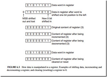
Examples of how a register can process data are shown in Figure 6.5. A binary word in a register can be shifted one or more bit positions to the right or left, or the register may be connected as an up/down counter so that it can be incremented (add one to the content) or decremented (subtract one from the content). A register can also be reset or cleared, thereby erasing any data in it and leaving the content zero.
Data transfers and manipulations performed on a register are initiated by individual computer instructions. For example, one instruction may cause the register to be loaded from a memory location. Another instruction may cause the word in the register to be transferred to a memory location. All data transfers are parallel, meaning that all bits are moved simultaneously from the source to the destination.
The main working register in most digital computers is called the accumulator. It may also be called the A register, W register, or something else.
The accumulator can hold one word whose bit length is equal to that of a memory location. An 8-bit microprocessor has an 8-bit accumulator. The accu- mulator is part of the ALU.
The accumulator can be loaded from memory or the accumulator content can be stored in any memory location. I/O operations with peripheral units sometimes also take place through the accumulator.
Data to be processed by the arithmetic/logic section is usually held in the accumulator. This data is fed to the ALU. The ALU is a digital logic circuit that can add, subtract, and perform a wide variety of logic operations.
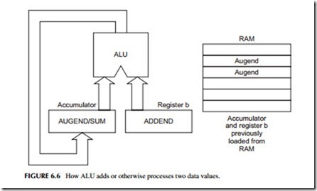
The ALU is capable of processing two inputs, one from the accumulator and one from the memory of another register (see Figure 6.6). Let’s assume that you wish to add two binary numbers. To do this, you first load one of the numbers (the augend) into the accumulator. This is done with a load- accumulator instruction that takes the number from a memory location and puts it into the accumulator. Next, an ADD instruction is executed. This causes another word (the addend) to be taken from memory and placed in register B. It is then added to the content of the accumulator. The sum is usually stored back in the accumulator, replacing the augend originally there.
Some microprocessors have two or more accumulator registers that share a single ALU. Two accumulators provide greater flexibility in the manipulation of data than a single accumulator. Such multiple registers simplify, speed up, and shorten a program to perform a given operation. Some sophisticated CPUs have 4, 8, 16, or even more accumulators. Usually they are referred to as GPRs or a register file. These registers can each use the ALU and act as temporary storage locations for data and the intermediate results of calculations. Instructions are provided to move data from one register to another.
In most micros, the GPRs share a single ALU. The ALU accepts only two input words and generates a single output word. The two words to be processed by the ALU usually come from any two GPRs or any GPR and a designated memory location. The destination of the ALU output can also be one of the GPRs in some CPUs.
Control Unit
CPUs also have several other registers, including the instruction register; the program counter, also called the instruction counter; and the memory address register, also called the address buffer.
The instruction register (IR) is used to store the instruction word. When the CPU fetches an instruction from memory, it is temporarily stored in the IR. The instruction is a binary word or code that defines a specific operation to be performed. The instruction word is also called the op code or operation code. The CPU decodes the instruction, and then executes it.
The program counter (PC) is really a counter and a register. It stores a binary word that is used as the address for accessing the instructions in a program. If a program begins with an instruction stored in memory location 43, the PC is first loaded with the address 43. The address in the PC is applied to the memory, causing the instruction in location 43 to be fetched and executed. After the instruction is executed, the PC is incremented (add 1) to the next address in sequence, or 44. The instructions in a program are stored in sequential memory locations.
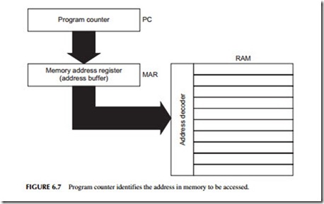
The memory address register (MAR) or address buffer also stores the address that references memory. This register directly drives the address bus and the memory address decoder in RAM or ROM. The MAR gets input from the PC when an instruction is to be accessed (see Figure 6.7 ). The MAR can also be loaded with an address that is used to access data words stored in memory. To retrieve a data word used in an arithmetic operation, the MAR is loaded with the binary word that points to the location of that word in RAM. This address is often a part of the instruction.
It is important to note that the PC and the MAR (address buffer) have a fixed length of so many bits. And that limits the amount of memory that can be accessed. For example, with a 16-bit address register, the address bus has 16 bits to address RAM and ROM. With 16 bits, a maximum of 216 = 65,536 words can be addressed.
There are usually two other registers, the flag and stack pointer registers. The flag or F register is an 8-bit register whose individual flip-flops are set and reset by the ALU as the various arithmetic and logic operations are carried out. Each flip-flop is called a flag. As an example, there are zero (Z) and carry (C) flags. If the accumulator content is zero after an operation is performed, the Z flag is set indicating this condition. If an arithmetic operation (addition) results in a carry from the MSB of the accumulator, the C flag is set indicating this
condition. These flags can be monitored or tested by the control circuitry to change the sequence of processing.
The stack register is a 16-bit or larger register used to address a selected area of RAM known as the stack. This memory is used to store register con- tents and status information when subroutines and interrupts are used.
Instruction-Word Formats
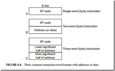
There are three types of instruction formats used in typical 8-bit microprocessors, illustrated in Figure 6.8. In the single-word format, the instruction is a single 8-bit word. This word is called the op code. The op code tells the ALU, the registers, and other elements of the system what to do. In this format, no address is used. The focus of the instruction is implied in the instruction. That is, the data to be processed is already in a location designated by the instruction. Usually the data is in a register. Typical instructions using this format are register-to-register transfer, shift data left (or right), or clear to zero.
The two-word instruction format in Figure 6.8 requires two 8-bit words to define the operation. These two words are stored in sequential memory locations. The first word is the op code. The second word is usually an address that specifies a memory location where the data word to be processed is stored. For example, if the op code calls for an add operation, the address word designates the location in RAM of the number to be added to the contents of the accumulator. The 256 bytes of RAM can be addressed with 1 byte of address.
In some 2-byte instructions, the second byte is not the address. Instead, it is the data itself. This is called an immediate instruction since it is not necessary to address the data that is available immediately within the instruction itself.
The three-word instruction format in Figure 6.8 is comprised of an 8-bit op code and two 8-bit address words stored in sequential memory locations. The second and third bytes together form a 16-bit address word that designates the location in RAM of the data to be processed. In the 3-byte instruction for- mat, the first byte is the op code, the second byte is the least significant half of the address, while the third byte is the most significant part of the address. Different formats are used by other micros.
To access a word in RAM, the instruction address word must be stored in the MAR. This happens during the instruction fetch operation. When an instruction is fetched from memory, the op code is stored in the instruction register while the address is stored in the MAR. The instruction is then executed. The MAR usually gets its input from the PC. Once an instruction is fetched and executed, the PC is incremented.
The PC may be incremented once, twice, or three times, depending on the length of the instruction just executed. If a 2-byte instruction is executed, the PC is incremented twice so that the PC points to the address of the next instruction op code.
Program Execution Example
Now let’s illustrate how a typical CPU executes a simple program. Here are a few common instructions similar to those found in any micro.
Move A to B (MOV B,A): This is a 1-byte instruction that causes the content of the accumulator (A) to be moved to register B. The content of the accumulator is not erased.
Load Accumulator (LDA): This is a 3-byte instruction that takes the content of the address specified by the second and third bytes and loads it into the accumulator.
Add Immediate (ADI): This is a 2-byte instruction that takes the content of the second byte of the instruction and adds it to the content of the accumulator. The sum is stored in the accumulator, replacing the number that was there previously.
Halt (HLT): Halt is a 1-byte instruction that stops processing.
Note that we refer to each instruction by a three-letter abbreviation called a mnemonic.
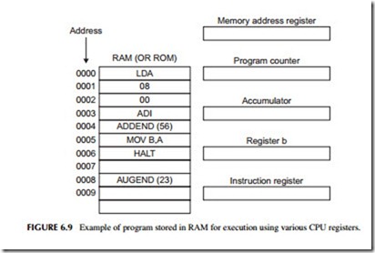
Figure 6.9 shows a complete CPU and the RAM containing a simple pro- gram. The first instruction in the program is the LDA stored in location 0000.
To begin the execution, the address of the first instruction is loaded into the PC that points to the location of the instructions in RAM.
Next, the content of the PC is transferred to the MAR that addresses RAM. The LDA instruction op code is fetched and stored in the instruction register. The address bytes of the LDA instruction in locations 0001 and 0002 are then transferred to the memory address register. The address of the data to be loaded into the accumulator in bytes 2 and 3 is 0008. The desired data word in location 0008 is retrieved and loaded into the accumulator. This is the augend (23).
After the LDA instruction is executed, the number 23 is stored in the accumulator. Next, the PC is incremented three times. The ADI instruction is then fetched and stored in the instruction register. The number to be added is stored in location 0004.
This is an ADD immediate instruction where the second byte contains the data, in this case the addend (56). The number in location 0004H is 56, which is added to 23 in the accumulator, creating the sum 79. The mnemonic of the next instruction to be executed is MOV B,A in location 0005.
The sum in the accumulator is then moved to the B register by the MOV B,A instruction. The content of the accumulator is not changed when data is transferred to the B register.
The PC is incremented once since the HLT is a 1-byte instruction.
As you can see by this step-by-step analysis of the execution of a computer program, there is nothing mysterious about its operation. The CPU simply fetches and then executes the sequentially stored instructions at very high speed until the operation is complete. This process is sometimes referred to as the stored program concept.
Microcomputer Buses
Data transfers inside a microprocessor take place in parallel. This means that all bits in a word are transferred simultaneously from one place to another. It takes only a few nanoseconds (one billionth of a second) for all data bits in one register to be moved to another register.
The parallel data transfers take place over a data bus. A bus is simply multiple parallel electrical connections from a source to a destination. A number of these buses are contained within the CPU and are known as internal buses.
Microprocessors usually have three major buses—a data bus, an address bus, and a control bus. These are made available to external circuits in some micros. A typical 8-bit CPU has an 8-bit data bus and a 16-bit address bus. The data bus sends data to and from the CPU, RAM, ROM, and I/O sections. All data transfers between the CPU and memory or I/O sections take place over the data bus. The address bus drives all of the memory and I/O devices.
When an instruction is fetched from RAM or ROM, it is transferred over the data bus from the memory into the instruction register. Any data word retrieved from memory or a peripheral device via the input section also passes over the data bus into the accumulator or GPR.
When a store instruction is executed, the word in the accumulator is transmitted over the data bus into RAM. Data can also be transferred from the accumulator over the data bus to an external device such as an LCD. Or, data from an input device such as a keyboard passes over the data bus and is placed into the accumulator. The important point here is that data can move in either direction over the data bus. We say that it is a bidirectional bus.
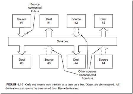
Another key point is that the data bus can be connected to only one data source at a time. Data can originate only at a single source, but it can be sent to one or more destinations. To accomplish this, circuits called bus multiplexers, or three-state line-driver circuits, are used to connect or disconnect the various data sources to or from the bus. Figure 6.10 illustrates this concept.
The address bus is a unidirectional bus. It transfers an address from the CPU to all external circuits (memory and I/O). Address words are produced in the CPU. The PC generates the address that points to the instruction to be fetched. The content of the PC is transferred over a parallel 16-bit internal
address bus to the memory address register or address buffer. The output of the MAR or address buffer is the address bus.
The control bus consists of numerous signals generated by the microprocessor and used to initiate various memory or I/O operations. The control bus also contains input lines from external circuits that tell the CPU what to do and when. The number of control signals varies from CPU to CPU.
