Circuit Arrangements
Five different approaches are in common use for moving coil PU input amplification.
Step-Up Transformer
This was the earliest method to be explored and was advocated by Ortofon, which was one of the pioneering companies in the manufacture of MC PU designs. The advantage of this system is that it is substantially noiseless, in the sense that the only source of wide-band noise will be the circuit impedance of the transformer windings and that the output voltage can be high enough to minimize the thermal noise contribution from succeeding stages.
The principal disadvantages with transformer step-up systems, when these are operated at very low signal levels, are their proneness to mains “hum” pick up, even when well shrouded, and their somewhat less good handling of “transients” because of the effects of stray capacitances and leakage inductance. Care in their design is also needed to overcome the magnetic nonlinearities associated with the core, which are particularly significant at low signal levels.
Systems Using Paralleled Input Transistors
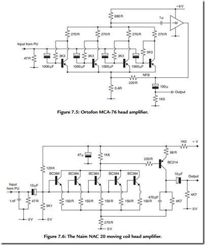
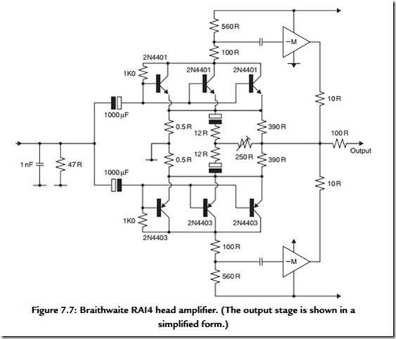
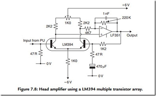
The need for a very low input circuit impedance to minimize thermal noise effects has been met in a number of commercial designs by simply connecting a number of small signal transistors in parallel to reduce their effective base-emitter circuit resistance. Designs of this type came from Ortofon, Linn/Naim, and Braithwaite and are shown in Figures 7.5–7.7.
If such small signal transistors are used without selection and matching—a time- consuming and expensive process for any commercial manufacturer—some means must be adopted to minimize the effects of the variation in base-emitter turn-on voltage that exist between nominally identical devices because of variations in the doping level in the silicon crystal slice or to other differences in manufacture.
This is achieved in the Ortofon circuit by individual collector-base bias current networks, for which the penalty is the loss of some usable signal in the collector circuit. In the
Linn/Naim and Braithwaite designs, this evening out of transistor characteristics in circuits having common base connections is achieved by the use of individual emitter resistors to swamp such differences in device characteristics. In this case, the penalty is that such resistors add to the base-emitter circuit impedance when the task of the design is to reduce this.
Monolithic Super-Matched Input Devices
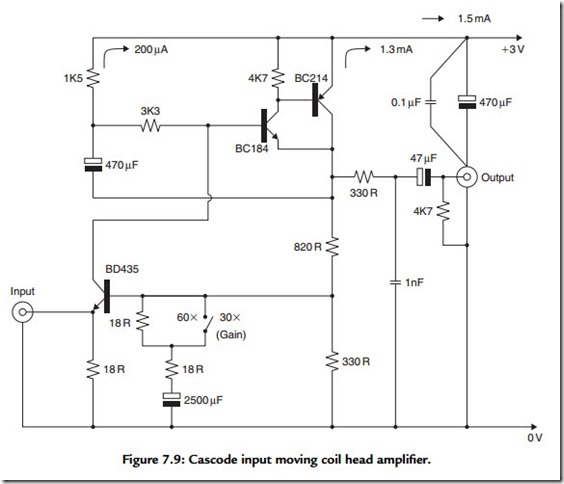
An alternative method of reducing the input circuit impedance, without the need for separate bias systems or emitter circuit-swamping resistors, is to employ a monolithic (integrated circuit type) device in which a multiplicity of transistors has been
simultaneously formed on the same silicon chip. Since these can be assumed to have virtually identical characteristics, they can be paralleled, at the time of manufacture, to give a very low impedance, low noise, matched pair.
An example of this approach is the National Semiconductors LM 194/394 super-match pair, for which a suitable circuit is shown in Figure 7.8. This input device probably offers the best input noise performance currently available, but is relatively expensive.
Small Power Transistors as Input Devices
The base-emitter impedance of a transistor depends largely on the size of the junction area on the silicon chip. This will be larger in power transistors than in small signal transistors, which mainly employ relatively small chip sizes. Unfortunately, the current gain of power transistors tends to decrease at low collector current levels, making them unsuitable for this application.
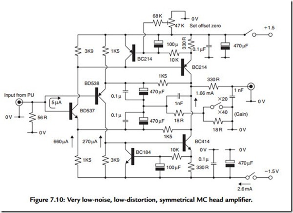
However, use of the plastic encapsulated medium power (3–4 A lc max.) styles, in T0126, T0127, and T0220 packages, at collector currents in the range of 1–3 mA, achieves a satisfactory compromise between input circuit impedance and transistor performance and allows the design of very linear low-noise circuitry. Two examples of MC head amplifier designs of this type, by the author, are shown in Figures 7.9 and 7.10.
The penalty in this case is that, because such transistor types are not specified for low noise operation, some preliminary selection of the devices is desirable, although, in the writer’s experience, the bulk of the devices of the types shown will be found to be satisfactory in this respect.
In the circuit shown in Figure 7.9, the input device is used in the common base (cascode) configuration so that the input current generated by the PU cartridge is transferred directly to the higher impedance point at the collector of this transistor so that the stage gain, prior to the application of negative feedback to the input transistor base, is simply the impedance transformation due to the input device.
In the circuit of Figure 7.10, the input transistors are used in a more conventional common-emitter mode, but the two input devices, although in a push–pull configuration, are effectively connected in parallel so far as the input impedance and noise figure are concerned. The very high degree of symmetry of this circuit assists in minimizing both harmonic and transient distortions.
Both of these circuits are designed to operate from 3-V DC “pen cell” battery supplies to avoid the introduction of mains hum due to the power supply circuitry or to earth loop effects. In mains-powered head amps, great care is always necessary to avoid supply line signal or noise intrusions in view of the very low signal levels at both the inputs and the outputs of the amplifier stage.
It is also particularly advisable to design such amplifiers with single point “0-V” line and supply line connections, which should be coupled by a suitable combination of good quality decoupling capacitors.
