Depletion Insulated Gate FETS (MOSFETs)
Insulated gate FETs do not use a P–N junction. Instead, they use a metal gate, which is electrically isolated from the semiconductor channel by a thin layer of oxide. This device is known as a metal-oxide semiconductor field effect transistor (MOSFET or MOST).
There are two important types of MOSFETs: N- type units with N channels and P-type units with P channels. N-type units with N channels are called depletion mode devices because they conduct when zero bias is applied to the gate. In the depletion mode, the electrons are conducting until the gate bias volt- age depletes them. The drain current is depleted as a negative bias is applied to the gate. P-type units with P channels are enhancement mode devices. In the enhancement mode, the electron flow is normally cut off until it is aided or enhanced by the bias voltage on the gate. Although P-channel depletion MOSFETs and N-channel enhancement MOSFETs exist, they are not commonly used.
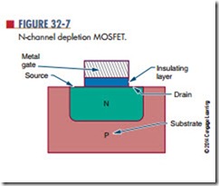
Figure 32-7 shows a cross section of a N-channel depletion MOSFET. It is formed by implanting an N channel in a P substrate. A thin insulating layer of silicon dioxide is then deposited on the channel, leaving the ends of the channel exposed to be attached to wires and act as the source and the drain. A thin metallic layer is attached to the insulating layer over the N channel. The metallic layer serves as the gate. An additional lead is attached to the substrate. The metal gate is insulated from the semiconductor channel so that the gate and the channel do not form a P–N junction. The metal gate is used to control the conductivity of the channel, as in the JFET.
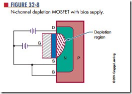
The MOSFET shown in Figure 32-8 has an N chan- nel. The drain is always made positive with respect to the source, as in the JFET. The majority carriers are electrons in the N channel, which allow drain current (ID) to flow from the source to the drain. As with the JFET, the drain current is controlled by the gate-to- source bias voltage (EGS). When the source voltage is 0, a substantial drain current flows through the device because a large number of majority carriers (electrons) are present in the channel. When the gate is made negative with respect to the source, the drain current decreases as the majority carriers are depleted. If the negative gate voltage is increased sufficiently, the drain current drops to 0. One difference between MOSFETs and JFETs is that the gate of the N-channel depletion MOSFET can also be made positive with respect to the source. This cannot be done with a JFET because it would cause the gate and channel P–N junction to be forward biased.
When the gate voltage of a depletion MOSFET is made positive, the silicon-dioxide insulating layer pre- vents any current from flowing through the gate lead. The input resistance remains high, and more majority carriers (electrons) are drawn into the channel, enhancing the conductivity of the channel. A positive gate voltage can be used to increase the MOSFET’s drain current, and a negative gate voltage can be used to decrease the drain current. Because a negative gate voltage is required to deplete the N-channel MOSFET, it is called a depletion mode device. A large amount of drain current flows when the gate voltage is equal to 0. All depletion mode devices are considered to be turned on when the gate voltage is equal to 0.
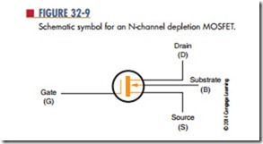
An N-channel depletion MOSFET is represented by the schematic symbol shown in Figure 32-9. Note that the gate lead is separated from the source and drain
leads. The arrow on the substrate lead points inward to represent an N-channel device. Some MOSFETs are constructed with the substrate connected internally to the source lead, and the separate substrate lead is not used.
A properly biased N-channel depletion MOSFET is shown in Figure 32-10. Note that it is biased the same way as an N-channel JFET. The drain-to-source volt- age (EDS) must always be applied so that the drain is positive with respect to the source. The gate-to-source voltage (EDS) can be applied with the polarity reversed. The substrate is usually connected to the source, either internally or externally. In special applications, the substrate may be connected to the gate or another point within the FET circuit.
A depletion MOSFET may also be constructed as a P-channel device. P-channel devices operate in the same manner as N-channel devices. The difference is that the majority carriers are holes. The drain lead is made negative with respect to the source, and the
interchanged. In special applications, the gate may be offset from the drain region to reduce capacitance between the gate and drain. When the gate is offset, the source and drain leads cannot be interchanged.
QUESTIONS
1. How does a MOSFET differ in construction from a JFET?
2. Describe how a MOSFET conducts a current.
3. What is the major difference in operation between a MOSFET and a JFET?
4. Draw and label schematic diagrams of P-channel and N-channel MOSFETs.
5. What leads can be interchanged on JFETs and MOSFETs?


