PROGRAMMABLE LOGIC DEVICES
There are two ways that digital devices are built today. The most common is to use an embedded controller or microcomputer. This is a single-chip computer that you can program to do whatever digital function you want. Most electronic products have at least one embedded controller at the heart of their design.
In some cases, the embedded controller is not fast enough to do the job. One way to make the circuitry is to use individual logic circuits such as gates, flip-flops (FFs), counters, and so on. That is the way it used to be done. Now, if you need fast custom digital logic, you build the circuit with a programmable logic device (PLD). A PLD is an IC that contains a mix of gates, FFs, and other circuits that can be programmed to implement any digital function. The programming is usually done on a computer and a file is created. The file is then downloaded to the PLD, where it is stored in a RAM or ROM. The file in the memory determines how the unique circuit is formed.
There are three basic types of PLDs: simple PLDs, complex PLDs, and field programmable gate arrays (FPGAs). The SPLDs are small devices for simpler digital circuits. The most common types are called programmable array logic (PAL), programmable logic arrays (PLAs), and generic array logic (GAL). PROMs are also used as SPLDs. For example, the address input to a ROM is some binary number or a collection of binary inputs. These form an address to locate a specific binary word stored in that location. When that particular selection of input bits occurs, it forms the address that identifies the memory location where the desired set of output responses is stored. This form of SPLD is also called a look-up table or LUT.
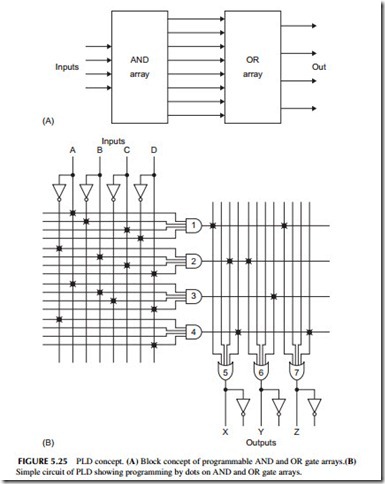
The other SPLDs are essentially a set of AND and OR gates that can be pro- grammed. They all take the form shown in Figure 5.25. You can select which inputs go to the AND gates, and/or select which AND outputs go to which OR gate inputs. A PROM has the AND array fixed and you can program the OR gates. A PAL is an SPLD in which you can program the AND inputs but the OR connections are fixed. A PLA is a PLD that lets you program both the AND inputs and the OR connections. In both PLAs and PALs, the programming is usually permanent.
A GAL is a variation of the PAL with its AND inputs programmable. The difference is that the programming can be changed. The program you develop is actually stored in flash memory. The flash memory cells send the program- ming bits to the various AND and OR gates telling them what logic to imple- ment. You can then erase it and reprogram if you want or need to. GALs also have one or more FFs associated with the logic gates, so you can store bits or actually build counters and registers by programming.
CPLDs are complex PLDs similar to SPLDs, only larger. They contain more gates and flip-flops so that very large logic projects can be built on a single chip. A typical CPLD is really just a large collection of PALs or GALs that can be individually programmed and then connected together with a large
interconnect matrix. Input/output (I/O) circuits also provide inversion if needed or extra power to drive external circuits. Again, flash memory is used to store the programming.
The largest and most flexible PLD is the field programmable logic array or FPGA. It has become the most popular and common way to implement digital equipment other than a microcontroller. FPGAs are large chips that contain thousands of logic circuits. The largest devices have millions of gates and other circuits. Most FPGAs are programmed by storing a bit pattern in the SRAM cells inside. These cells tell the logic circuits what configuration to take and what functions to perform. If you turn the power off, the programming goes away and all you have is a dumb FPGA with no logic interconnections or func- tions. When you power up an FPGA, the desired program, usually from a flash memory, or a computer loads the RAM cells with the program, thereby enabling the FPGA to perform its desired function.
The logic inside an FPGA is essentially thousands of look-up tables (LUTs) that can be individually programmed. Each LUT has its own program memory block as well as one or more FFs and I/O circuits. The LUTs may also be interconnected to one another by programming. With this arrangement virtually any digital logic operation can be programmed. You can even make your own custom computer with an FPGA, for example.
There are about a half-dozen companies that make PLDs. The two oldest and largest are Xilinx and Altera. Both have extensive lines of CPLDs and FPGAs.
