Insulated Gate FETs (MOSFETs)
Insulated gate FET devices, usually called MOSFETs, are by far the most widely available, and most widely used, of all the field effect transistors. They normally have a
rather worse noise figure than an equivalent JFET, but, on the plus side, they have rather more closely controlled operating characteristics. The range of types available covers the very small-signal, low-working voltage components used for VHF amplification in TVs and FM tuners (for which applications a depletion-mode dual-gate device has been introduced that has very similar characteristics to those of an RF pentode valve) to high- power, high-working voltage devices for use in the output stages of audio amplifiers, as well as many other high-power and industrial applications. They are made in both depletion- and enhancement-mode forms (the former having gate characteristics similar to that of the JFET, whereas the latter description refers to the style of device in which there is normally no drain current in the absence of any forward gate bias), in N-channel and P-channel versions, and, at the present time, in voltage and dissipation ratings of up to 1000 V and 600 W, respectively.
All MOSFETs operate in the same manner, in which a conducting electrode (the gate) situated in proximity to an undoped layer of very high purity single-crystal silicon (the channel), but separated from it by a very thin insulating layer, is caused to induce an electrostatic charge in the channel, which will take the form of a layer of mobile electrons or holes. In small-signal devices this channel is formed on the surface of the chip between two relatively heavily doped regions, which will act, respectively, as the source and the drain of the FET, while the conducting electrode will act as the current controlling gate.
Although modern photolithographic techniques are capable of generating exceedingly precise diffusion patterns, the length of the channel formed by surface-masking techniques in a lateral MOSFET will be too long to allow a low channel “on” resistance. For high current applications, the semiconductor manufacturers have therefore evolved a range of vertical MOSFETs. In these, very short channel lengths are achieved by sequential diffusion processes from the surface, which are then followed by etching a V- or U-shaped trough inward from the surface so that the active channel is formed across the exposed edge of a thin diffused region. Because this channel is short in length, its resistance will be low, and because the manufacturers generally adopt device structures that allow a multiplicity of channels to be connected electrically in parallel, channel “on” resistances as low as 0.008 Ω have been achieved.
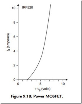
Like a JFET, the MOSFET would, left to itself, have a square-law relationship between gate voltage and drain current. However, in practice, this is affected by the device geometry, and many modern devices have a quite linear Id/Vg characteristic, as shown in Figure 9.18 for an IRF520 power MOSFET.
The basic problem with the MOSFET is that of gate/channel overvoltage breakdown, in which the thin insulating layer of silicon oxide or silicon nitride between the gate electrode and the channel breaks down. If this happens the gate voltage will no longer
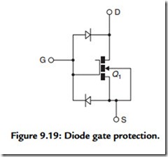
control the drain current and the device is defunct. Because it is theoretically possible for an inadvertent electrostatic charge, such as might arise with respect to the ground if a user were to wear nylon or polyester fabric clothing and well-insulated shoes, it is common practice in the case of small-signal MOSFETs for protective diodes to be formed on the chip at the time of manufacture. These could be either zener diodes or simple junction diodes connected between the gate and the source or the source and drain, as shown in Figure 9.19.
In power MOSFETs, these protective devices are seldom incorporated into the chip. There are two reasons for this: (1) that the effective gate/channel area is so large that the associated capacitance is high, which would then require a relatively large inadvertently applied static charge to generate a destructive gate/channel voltage (typically >40 V), and (2) that such protective diodes could, if they were triggered into conduction, cause the MOSFET to act as a four-layer thyristor and become an effective electrical short circuit. However, there are usually no performance penalties that will be incurred by connecting some external protective zener diode in the circuit to prevent the gate/source or gate/drain voltage exceeding some safe value; this is a common feature in the output stages of audio power amplifiers using MOSFETs.
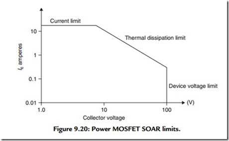
Apart from the possibility of gate breakdown, which, in power MOSFETs, always occurs at less than the maker’s quoted voltage, except at zero drain current, MOSFETs are quite robust devices, and the safe operating area rating (SOAR) curve of these devices, shown for a typical MOSFET in Figure 9.20, is free from the threat of secondary breakdown whose limits are shown, for a power BJT, in Figure 9.12. The reason for this freedom
from localized thermal breakdown in the MOSFET is that the mobility of the electrons (or holes) in the channel decreases as the temperature increases, which gives all FETs a positive temperature coefficient of channel resistance.
Although it is possible to propose a mathematical relationship between gate voltage and drain current, with MOSFETs as was done in the case of the JFET, the manufacturers tend to manipulate the diffusion pattern and construction of the device to linearize its operation, which leads to the type of performance (quoted for an actual device) shown in Figure 9.21. However, as a general rule, the gfs of a MOSFET will increase with drain current, and a forward transconductance (slope) of 10 S/A is quoted for an IRF140 at an ID value of 15 A.


