Junction Field Effect Transistors ( JFETs)
JFETs are, almost invariably, depletion mode devices, which means that there will be some drain current at a zero-applied gate-source potential. This current will decrease in a fairly linear manner as the reverse gate-source potential is increased, giving an operating characteristic, which is, in the case of an N-channel JFET, very similar to that of a triode valve, as shown in curve ‘c’ of Figure 9.3. Like a thermionic valve, the operation of the device is limited to the range between drain (or anode) current cutoff and gate (or grid) current. In the case of the JFET, this is because the gate-channel junction is effectively a silicon junction diode—normally operated under reverse bias conditions. If the gate source voltage exceeds some 0.6 V in the forward direction, it will conduct, which will prevent gate voltage control of the channel current.
P-channel JFETs are also made, although in a more limited range of types, and these have what is virtually a mirror image of the characteristics of their N-channel equivalents, although in this case the gate-source forward conduction voltage will be of the order of -0.6 V, and drain current cutoff will occur in the gate voltage range of +3 to +8 V. Although Sony did introduce a range of junction FETs for power applications, these are no longer available, and typical contemporary JFETs cover the voltage range (maximum) from 15 to 50 V, mainly limited by the gate-drain reverse breakdown potential, and with permitted dissipations in the range 250–400 mW. Typical values of gm (usually called gfs in the case of JFETs) fall in the range of 2–6 mS.
JFETs mainly have good high-frequency characteristics, particularly the N-channel types, of which there are some designs capable of use up to 500 MHz. Modern types can also offer very low noise characteristics, although their very high input impedance will lead to high values of thermal noise if their input circuitry is also of high impedance; however, this is within the control of the circuit designer. The internal noise resistance of a JFET, R(n), is related to the gfs of the device by
and the value of gfs can be made higher by paralleling a number of channels within the chip. The Hitachi 2SK389 dual matched-pair JFET achieves a gfs value of 20 mS by this technique, with an equivalent channel thermal noise resistance of 33 ohms.
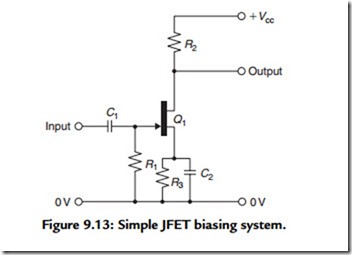
Although JFETs will work in most of the circuit layouts shown for junction transistors, the most significant difference in the circuit structure is due to their different biasing needs. In the case of a depletion mode device it is possible to use a simple source bias arrangement, similar to the cathode bias used with an indirectly heated valve, of the kind shown in Figure 9.13. As before, the source resistor, R3, will need to be bypassed with a capacitor, C2, if the loss of stage gain due to local NFB is to be avoided. As with a
pentode valve, which the junction FET greatly resembles in its operational characteristics, the simplest way of calculating stage gain is by the relationship:
The device manufacturers will frequently modify the structure of the JFET to linearize its Vg/Id characteristics, but, in an ideal device, these will have a square-law relationship, as defined by
For a typical JFET operating at 2 mA drain current, the gfs value will be of the order of 1–4 mS, which would give a stage gain of up to 40 if R2, in Figure 9.13, is 10 kΩ. This is very much lower than would be given by a BJT and is the main reason why they are not often used as voltage-amplifying devices in audio systems unless their very high input impedance (typical values are of the order of 1012 Ω) or their high, and largely constant, drain impedance characteristics are advantageous.
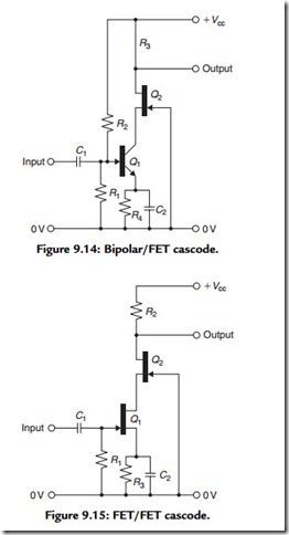
The real value of the JFET emerges in its use with other devices, such as the bipolar/FET cascode shown in Figure 9.14 or the FET/FET cascode layout of Figure 9.15. In the first of these, use of the JFET in the cascode connection confers the very high output impedance of the JFET and the high degree of output/input isolation characteristic of the cascode
layout, coupled with the high stage gain of the BJT. The source potential of the JFET (Q2) will be determined by the reverse bias appearing across the source/gate junction, and could typically be of the order of 2–5 V, which will define the collector potential applied to Q1. A further common application of this type of layout is that in which the cascode FET (Q2 in Figure 9.15) is replaced by a high-voltage BJT. The purpose of this
arrangement is to allow a JFET amplifier stage to operate at a much higher rail voltage than would be allowable to the FET on its own; this layout is often found as the input stage of high-quality audio amps.
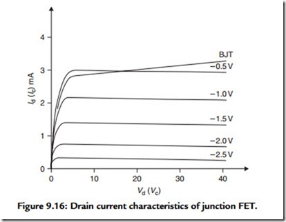
A feature that is very characteristic of the JFET is that for drain potentials above about 3 V, the drain current for a given gate voltage is almost independent of the drain voltage, as shown in Figure 9.16. BJTs have a high characteristic collector impedance, but their Ic/Vc curve for a fixed base voltage, also shown, for comparison, in Figure 9.16, is not as flat as that of the JFET. The very high dynamic impedance of the JFET resulting from this very flat Id/Vd relationship encourages the use of these devices as constant current sources, shown in Figure 9.17. In this form the JFET can be treated as a true two-terminal device, from which the output current can be adjusted, with a suitable JFET, over the range of several milliamperes down to a few microamperes by means of RV1.


