8051 Microcontroller Hardware

Introduction

The first task faced when learning to use a new computer is to become familiar with the capability of the machine. The features of the computer are best learned by studying the internal hardware design, also called the architecture of the device, to determine the type, number, and size of the registers and other circuitry.

The hardware is manipulated by an accompanying set of program instructions, or software, which is usually studied next. Once familiar with the hardware and software, the system designer can then apply the microcontroller to the problems at hand.

A natural question during this process is "What do I do with all this stuff?" Similar to attempting to write a poem in a foreign language before you have a vocabulary and rules of grammar, writing meaningful programs is not possible until you have become ac­quainted with both the hardware and the software of a computer.

This chapter provides a broad overview of the architecture of the 8051 . In subsequent chapters, we will cover in greater detail the interaction between the hardware and the software.

8051 Microcontroller Hardware

The 8051 microcontroller actually includes a whole family of microcontrollers that have numbers ranging from 8031 to 8751 and are available in N-Channel Metal Oxide Silicon (NMOS) and Complementary Metal Oxide Silicon (CMOS) construction in a variety of package types. An enhanced version of the 8051. the 8052, also exists with its own family of variations and even includes one member that can be programmed in BASIC. An inspection of Appendix E shows that there are dozens of other variations on the “core” 8051 architecture .This gal­axy of parts, the result of desires by the manufacturers to leave no market niche unfilled. would require many topics to cover.

8051 Microcontroller Hardware

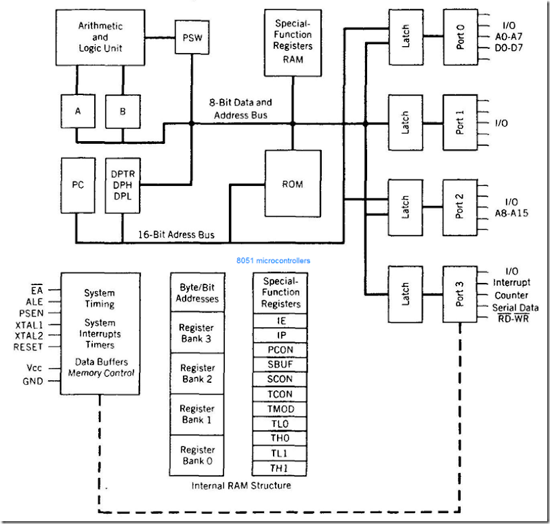
In this topic , we will study a "generic" 8051. housed in a 40-pin DIP. and direct the investigation of a particular type to the data books. The block diagram of the 8051 in Figure l a shows all of the features unique to micro­controllers:

Internal ROM and RAM

I/O ports with programmable pins Timers and counters

Serial data communication

The figure also shows the usual CPU components: program counter, ALU, working regis­ters, and clock circuits.

The 8051 architecture consists of these specific features:

Eight-bit CPU with registers A (the accumulator) and B

Sixteen-bit program counter (PC) and data pointer (DPTR)

Eight-bit program status word (PSW)

Eight-bit stack pointer (SP)

Internal ROM or EPROM (8751) of 0 (8031) to 4K (8051)

Internal RAM of 128 bytes:

Four register banks, each containing eight registers

Sixteen bytes, which may be addressed at the bit level

Eighty bytes of general-purpose data memory

Thirty-two input/output pins arranged as four 8-bit ports: PO-P3

Two 16-bit timer/counters: TO and TI

Full duplex serial data receiver/transmitter: SBUF

Control registers: TCON, TMOD, SCON, PCON, IP, and IE

Two external and three internal interrupt sources

Oscillator and clock circuits . Knowledge of the details of circuit operation that cannot be affected by any instruction or external data. while intellectually stimulating. tends to confuse the student new to the 8051. For this reason. this text will concentrate on the essential features of the R051: the more advanced student may wish to refer to manufacturers’ data books for additional information.

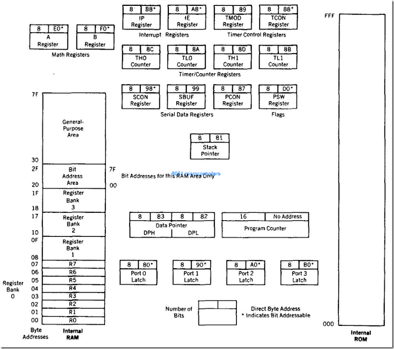
The programming model of the 8051 in Figure 1 b shows the 8051 as a collection of 8- and 16-bit registers and 8-bit memory locations. These registers and memory locations can be made to operate using the software instructions that are incorporated as part of the design. The program instructions have to do with the control of the registers and digital data paths that are physically contained inside the 8051, as well as memory locations that are physically located outside the 8051 .

The model is complicated by the number of special-purpose registers that must be present to make a microcomputer a microcontroller. A cursory inspection of the model is recommended for the first-time viewer; return to the model as needed while progressing through the ‘remainder of the text.

Most of the registers have a specific function; those that do occupy an individual block with a symbolic name, such as A or TH0 or PC. Others, which are generally indis­tinguishable from each other, are grouped in a larger block, such as internal ROM or RAM memory.

Each register, with the exception of the program counter, has an internal l-byte ad­dress assigned to it. Some registers (marked with an asterisk * in Figure 1b) are both byte and bit addressable. That is, the entire byte of data at such register addresses may be read or altered, or individual bits may be read or altered. Software instructions are gener­ally able to specify a register by its address, its symbolic name, or both.

8051 Microcontroller Hardware 2

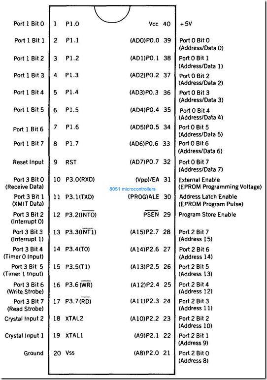
A pinout of the 8051 packaged in a 40-pin DIP is shown in Figure 2 with the full and abbreviated names of the signals for each pin. It is important to note that many of the pins are used for more than one function (the alternate functions are shown in parentheses in Figure 2). Not all of the possible 8051 features may be used at the same time.

8051 Microcontroller Hardware 3 

Programming instructions or physical pin connections determine the use of any multi­function pins. For example, port 3 bit 0 (abbreviated P3.0) may be used as a general­-purpose I/O pin, or as an input (RXD) to SBUF, the serial data receiver register. The system designer decides which of these two functions is to be used and designs the hard­ware and software affecting that pin accordingly.

The 8051 Oscillator and Clock

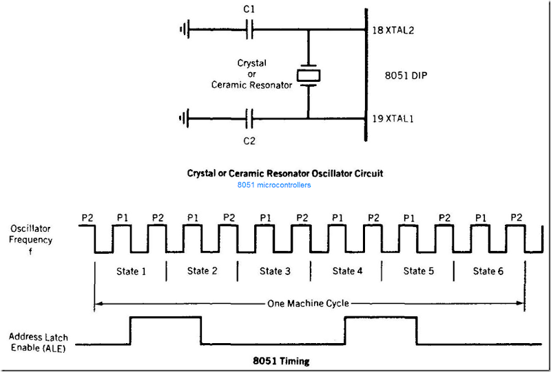
The heart of the 8051 is the circuitry that generates the clock pulses by which all internal operations are synchronized. Pins XTALI and XTAL2 are provided for connecting a reso­nant network to form an oscillator. Typically, a quartz crystal and capacitors are em­ployed, as shown in Figure 3. The crystal frequency is the basic internal clock fre­quency of the microcontroller. The manufacturers make available 8051 designs that can run at specified maximum and minimum frequencies, typically I megahertz to 16 mega­hertz. Minimum frequencies imply that some internal memories are dynamic and must always operate above a minimum frequency, or data will be lost.

8051 Microcontroller Hardware 4

Serial data Communication needs often dictate the frequency of the oscillator due to the require­ment that internal counters must divide the basic clock rate to yield standard communica­tion bit per second (baud) rates. If the basic clock frequency is not divisible without a remainder. then the resulting communication frequency is not standard.

Ceramic resonators may be used as a low-cost alternative to crystal resonators. How­ever, decreases in frequency stability and accuracy make the ceramic resonator a poor choice if high-speed serial data communication with other systems, or critical timing, is to be done.

The oscillator formed by the crystal, capacitors, and an on-chip inverter generates a pulse train at the frequency of the crystal, as shown in Figure 3.

The clock frequency, f. establishes the smallest interval of time within the micro­controller, called the pulse, P, time. The smallest interval of time to accomplish any simple instruction, or part of a complex instruction, however, is the machine cycle. The machine cycle is itself made up of six states. A state is the basic time interval for discrete operations of the microcontroller such as fetching an opcode byte, decoding an opcode, executing an opcode, or writing a data byte. Two oscillator pulses define each state.

Program instructions may require one, two, or four machine cycles to be executed. depending on the type of instruction. Instructions are fetched and executed by the micro­controller automatically, beginning with the instruction located at ROM memory address 0000h at the time the microcontroller is first reset.

To calculate the time any particular instruction will take to be executed, find the num­ber of cycles, C. from the list in Appendix A. The time to execute that instruction is then found by multiplying C by 12 and dividing the product by the crystal frequency:

8051 Microcontroller Hardware 5

For example, if the crystal frequency is 16 megahertz. then the time to execute an ADD A, RI one-cycle instruction is .75 microseconds. A 12 megahertz crystal yields the con­venient time of one microsecond per cycle. An 11.0592 megahertz crystal, while seem­ingly an odd value, yields a cycle frequency of 921.6 kilohertz, which can be divided evenly by the standard communication baud rates of 19200, 9600, 4800, 2400, 1200, and 300 hertz.

Program Counter and Data Pointer

The 8051 contains two 16-bit registers: the program counter (PC) and the data pointer (DPTR). Each is used to hold the address of a byte in memory.

Program instruction bytes are fetched from locations in memory that are addressed by the PC. Program ROM may be on the chip at addresses 0000h to OFFFh, external to the chip for addresses that exceed 0FFFh, or totally external for all addresses from 0000h to FFFFh. The PC is automatically incremented after every instruction byte is fetched and may also be altered by certain instructions. The PC is the only register that does not have an internal address.

The DPTR register is made up of two 8-bit registers. named DPH and DPL, that are used to furnish memory addresses for internal and external code access and external data access. The DPTR is under the control of program instructions and can be specified by its 16-bit name, DPTR, or by each individual byte name, DPH and DPL. DPTR does not have a single internal address; DPH and DPL are each assigned an address.

A and B CPU Registers

The 8051 contains 34 general-purpose, or working. registers. Two of these, registers A and B, comprise the mathematical core of the 8051 central processing unit (CPU). The other 32 are arranged as part of internal RAM in four banks, B0-B3. of eight registers and comprise the mathematical core .

The A (accumulator) register is the most versatile of the two CPU registers and is used for many operations. including addition, subtraction, integer multiplication and divi­sion, and Boolean bit manipulations. The A register is also used for all data transfers be­tween the 8051 and any external memory. The B register is used with the A register for multiplication and division operations and has no other function other than as a location where data may be stored.

Flags and the Program Status Word (PSW)

Flags are 1-bit registers provided to store the results of certain program instructions. Other instructions can test the condition of the flags and make decisions based upon the flag states. In order that the flags may be conveniently addressed, they are grouped inside the program status word (PSW) and the power control (PCON) registers.

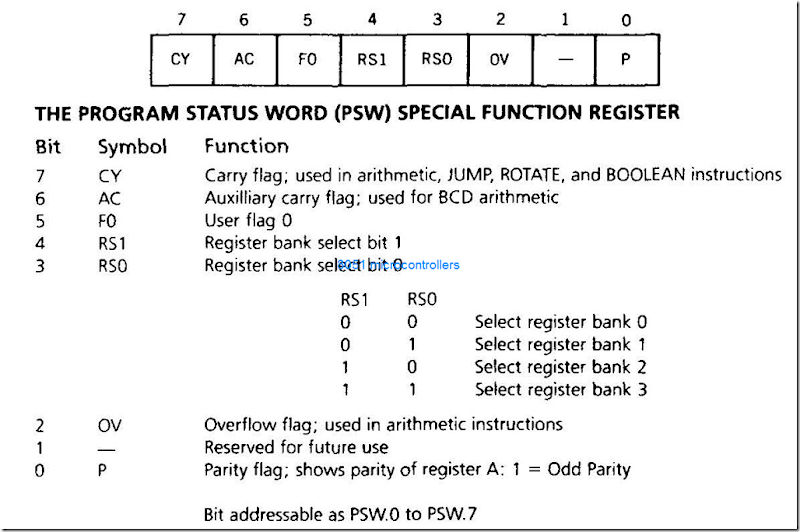
The 8051 has four math flags that respond automatically to the outcomes of math operations and three general-purpose user flags that can be set to I or cleared to 0 by the programmer as desired. The math flags include carry (C), auxiliary carry (AC), overflow (OY), and parity (P). User flags are named FO, GFO, and GFI; they are general-purpose flags that may be used by the programmer to record some event in the program. Note that all of the flags can be set and cleared by the programmer at will. The math Hags, however, are also affected by math operations .

The program status word is shown in Figure 4. The PSW contains the math flags, user program Hag FO, and the register select bits that identify which of the four general-­purpose register banks is currently in use by the program. The remaining two user flags, GFO and GFI, are stored in PCON, which is shown in Figure 13.

8051 Microcontroller Hardware 6 

Detailed descriptions of the math Hag operations will be discussed in topics that cover the opcodes that affect the flags. The user flags can be set or cleared using data move instructions will be covered .

Internal Memory

A functioning computer must have memory for program code bytes, commonly in ROM, and RAM memory for variable data that can be altered as the program runs. The 8051 has internal RAM and ROM memory for these functions. Additional memory can be added externally using suitable circuits.

Unlike microcontrollers with Von Neumann architectures, which can use a single memory address for either program code or data, but not for both, the 8051 has a Harvard architecture, which uses the same address, in different memories, for code and data. In­ternal circuitry accesses the correct memory based upon the nature of the operation in progress.

Internal RAM

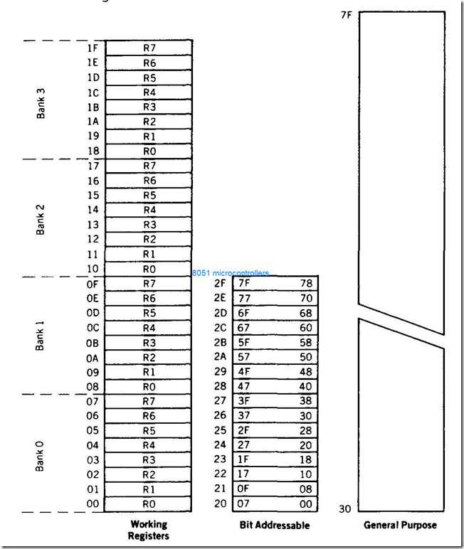
The 128-byte internal RAM, which is shown generally in Figure 1 and in detail in Fig­ure 5, is organized into three distinct areas:

1. Thirty-two bytes from address 00h to 1 Fh that make up 32 working registers or­ganized as four banks of eight registers each. The four register banks are num­bered 0 to 3 and are made up of eight registers named R0 to R 7. Each register can be addressed by name (when its bank is selected) or by its RAM address. Thus R0 of bank 3 is R0 (if bank 3 is currently selected) or address 18h (whether bank 3 is selected or not). Bits RS0 and RS 1 in the PSW determine which bank of registers is currently in use at any time when the program is running. Register banks not selected can be used as general-purpose RAM. Bank 0 is selected upon reset.

8051 Microcontroller Hardware 7

2. A bit-addressable area of 16 bytes occupies RAM byte addresses 20h to 2Fh, forming a total of 128 addressable bits. An addressable bit may be specified by its bit address of 00h to 7Fh, or 8 bits may form any byte address from 20h to 2Fh. Thus. for example, bit address 4Fh is also bit 7 of byte address 29h. Ad­dressable bits are useful when the program need only remember a binary event (switch on, light off, etc.). Internal RAM is in short supply as it is, so why use a byte when a bit will do?

3. A general-purpose RAM area above the bit area, from 30h to 7Fh, addressable as bytes.

The Stack and the Stack Pointer

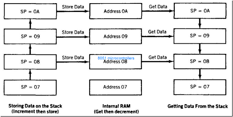
The stack refers to an area of internal RAM that is used in conjunction with certain op­codes to store and retrieve data quickly. The 8-bit stack pointer (SP) register is used by the 8051 to hold an internal RAM address that is called the "top of the stack." The address held in the SP register is the location in internal RAM where the last byte of data was stored by a stack operation.

When data is to be placed on the stack, the SP increments before storing data on the stack so that the stack grows up as data is stored. As data is retrieved from the stack, the byte is read from the stack, and then the SP decrements to point to the next available byte of stored data.

Operation of the stack and the SP is shown in Figure 6. The SP is set to 07h when the 8051 is reset and can be changed to any internal RAM address by the programmer.

The stack is limited in height to the size of the internal RAM. The stack has the poten­tial (if the programmer is not careful to limit its growth) to overwrite valuable data in the register banks, bit-addressable RAM, and scratch-pad RAM areas. The programmer is responsible for making sure the stack does not grow beyond pre-defined bounds!

The stack is normally placed high in internal RAM, by an appropriate choice of the number placed in the SP register, to avoid conflict with the register, bit, and scratch-pad internal RAM areas.

8051 Microcontroller Hardware 8

Special Function Registers

The 8051 operations that do not use the internal 128-byte RAM addresses from 00h to 7Fh are done by a group of specific internal registers. each called a special-function register (SFR). which may be addressed much like internal RAM. using addresses from 80h to FFh .

Some SFRs (marked with an asterisk * in Figure 1b) are also bit addressable. as is the case for the bit area of RAM. This feature allows the programmer to change only what needs to be altered. leaving the remaining bits in that SFR unchanged.

Not all of the addresses from 80h to FFh are used for SFRs. and attempting to use an address that is not defined. or "empty." results in unpredictable results. In Figure 2. I b, the SFR addresses are shown in the upper right corner of each block. The SFR names and equivalent internal RAM addresses are given in the following list :

NAME

FUNCTION

INTERNAL RAM ADDRESS (HEX)

A

Accumulator

OEO

B

Arithmetic

0F0

DPH

Addressing external memory

83

DPl

Addressing external memory

82

IE

Interrupt enable control

0A8

IP

Interrupt priority

0B8

PO

Input/output port latch

80

Pl

Input/output port latch

90

P2

Input/output port latch

A0

P3

Input/output port latch

0B0

PC ON

Power control

87

PSW

Program status word

0D0

SCON

Serial port control

98

SBUF

Serial port data buffer

99

SP

Stack pointer

81

TMOD

Timer / counter mode control

89

TCON

Timer / counter control

88

TLO

Timer 0 low byte

8A

THO

Timer 0 low byte

8C

TL1

Timer 0 low byte

8B

TH1

Timer 1 high byte

8D

Note that the PC is not part of the SFR and has no internal RAM address . see also Appendix F

SFRs are named in certain opcodes by their functional names, such as A or TH0, and are referenced by other opcodes by their addresses, such as 0E0h or 8Ch. Note that any address used in the program must start with a number; thus address E0h for the A SFR begins with 0. Failure to use this number convention will result in an assembler error when the program is assembled.

Internal ROM

The 8051 is organized so that data memory and program code memory can be in two entirely different physical memory entities. Each has the same address ranges.

The structure of the internal RAM has been discussed previously. A corresponding block of internal program code, contained in an internal ROM, occupies code address space 0000h to 0FFFh. The PC is ordinarily used to address program code bytes from addresses 0000h to FFFFh. Program addresses higher than 0FFFh, which exceed the internal ROM capacity, will cause the 8051 to automatically fetch code bytes from external program memory. Code bytes can also be fetched exclusively from an external memory, addresses 0000h to FFFFh, by connecting the external access pin (EA pin 31 on the DIP) to ground. The PC does not care where the code is; the circuit designer decides whether the code is found totally in internal ROM, totally in external ROM, or in a combination of internal and external ROM.
 

SUMMARY of MPU memory and I/O

SUMMARY

In this chapter, we examined the requirements of the Microprocessor Unit (MPU) to communicate with memory and I/O devices and to process binary data. Based on those requirements, we designed a generalized model of the

M PU. We discussed memory in terms of its storage elements, namely, latches and registers and techniques of assigning addresses. The steps required for the MPU to communicate with memory and I/Os were briefly described. The impor­tant concepts are summarized as follows.

· The MPU performs four primary operations: Memory Read, Memory Write, I/O Read, and I/O Write.

· To communicate with memory and I/Os, the MPU needs three types of buses: the unidirectional address bus to send memory and I/O addresses, the bidirec­tional data bus to transfer data, and control signals to enable the devices.

· The MPU should have signal lines to accept and to acknowledge external re­quests. These requests are Reset (go back to beginning), interrupt ( stop the ongoing process and attend to something urgent). wait to synchronize with slow memory, and allow the use of buses to an external device because the MPU response time is slower than that of the external device.

· To process data, the MPU should include registers to store data, memory pointers to hold memory addresses, ALU to perform arithmetic and logic op­erations, and flags to indicate data conditions.

· Memory is a group of registers, arranged in a sequence, to store bits. The number of cells (latches) in a register determines the size of the memory word in a chip.

· A memory chip requires address lines to identify a memory register, Chip Se­lect signal to select the chip, and control signals to read from and write into memory registers.

· The range of memory addresses assigned to a memory chip is done through

· the Chip Select logic.

· An I/O device can be identified either with an 8-bit address called the peripheral-mapped I/O or with a 16-bit address called the memory-mapped I/O.

· To communicate with memory or I/O, the MPU places the address of the de­vice on the address bus, sends the appropriate control signal, and places (or receives) data on the data bus.

Looking Ahead

In this topic , we examined the microprocessor as a programmable logic de­vice and developed a generalized model. Similarly, we discussed memory as a storage element and constructed a memory model. We examined briefly the role of l/Os as channels of communication with "the outside world." These three elements were interconnected through a bus architecture to form a model of a microprocessor-based system. Then we discussed how the MPU communicates with memory and I/Os.

In the next three chapters, we will explore each component and its com­munication process separately with details and specific examples. In Chapter 3. we will examine the Z80 microprocessor in the context of our generalized model of a programmable logic device. Chapter 4 discusses memory and its interfacing. and Chapter 5 is devoted to interfacing I/O devices.

ASSIGNMENTS

1. List the four operations commonly performed by the MPU .

2. What is a bus?

3. What is the function of the address bus?

4. How many memory locations can be addressed by the MPU with thirteen address lines?

S. How many address lines are necessary to address two megabytes (2048K) of memory?

6. What is the function of the interrupt signal and when is it used?

7. When is the bus request signal used?

8. Specify the number of registers and memory cells in a 128 x 4 memory chip.

9. How many bits are stored by a 256 x 4 memory chip? Can this chip be specified as 128-byte memory?

10. If the memory size is 1024 x 4 bits, how many chips are required to make J K-byte of memory?

11. If the memory chip size is 1024 x I bits, how many chips are necessary to make 4K (4,096) bytes of memory?

12. What is the function of the WR’ signal on the memory chip?

13. How many address lines are necessary for the memory chip with 2048 x 8 size?

14. How many address lines are necessary for the memory chip with 2048 x 4 size?

I5. The memory address range of a 4K (4,096)-byte memory chip begins at the

location 8000H Specify the entire memory address range and the number of pages in the chip.

16. The memory address of the last location of an 8K-byte memory chip is FFFFH . Find the starting address.

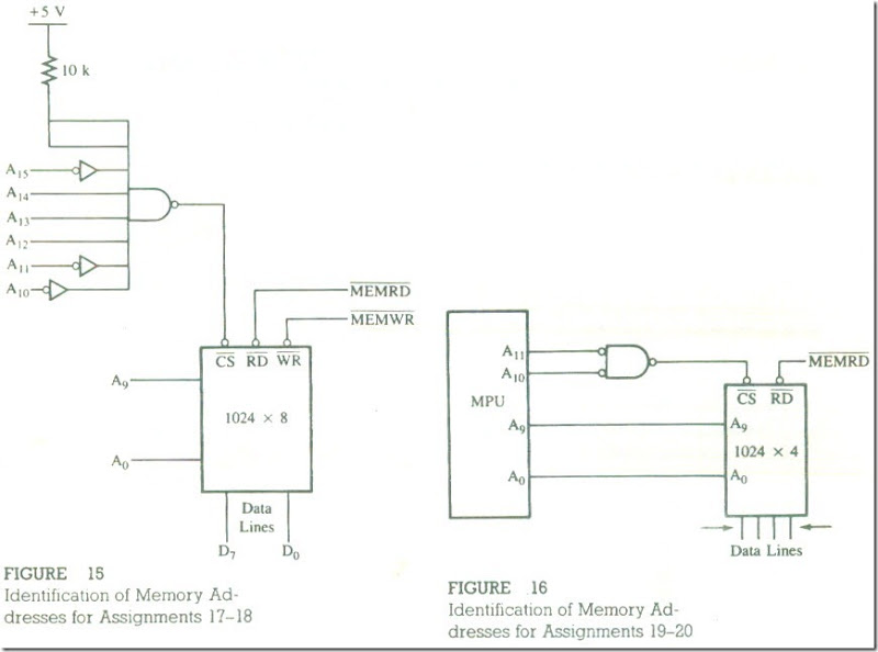
17. Identify the memory address range in Figure 15. List the high-order and low-order address lines. How many pages of memory does the chip include?

18. In Figure 2.IS, identify the address range if the inverter of the address line AIS is eliminated and AIS is connected directly to the NAND gate.

19. Figure 2.16 shows an MPU with the address bus containing 12 address lines and the data bus with four data lines; it is interfaced with the 1024 x 4 memory chip. Find the memory address range.

20. Specify the size of the memory word shown in Figure 16.

SUMMARY-23_03

FIGURE 15  Identification of Memory Ad­dresses for Assignments 17-18                                                    FIGURE 16 Identification of Memory Ad­dresses for Assignments 19-20


EXAMPLE OF A MICROPROCESSOR-BASED SYSTEM

EXAMPLE OF A MICROPROCESSOR-BASED SYSTEM

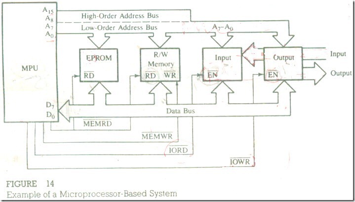
In the last three sections, we discussed a generalized MPU model. prime memory and its organization model. and I/Os. The discussion can be summarized in the block diagram of a microprocessor-based system as shown in Figure 14. It in­cludes a generalized MPU, two types of prime memory. and two I/O devices.

All address lines are used to address memory. and only the low-order ad­dress bus is used to identify I/O devices, indicating that they are connected as peripheral-mapped I/O (the details of Chip Select decoding are omitted here). The

MICROPROCESSOR-BASED SYSTEM: MPU, MEMORY, AND I/O

data bus is bidirectional and common to all devices. The four control signals gen­erated by the MPU are connected to different peripheral!" as shown in Figure 2.14.

HOW DOES THE SYSTEM WORK?

Let us assume that a simple program with three instructions is already written and stored in binary in R/W memory. Those instructions are

1. Read on/off switches at input port No. 20H (H stands for hexadecimal.)

2. Turn on the devices corresponding to on switches at the output port 80H  

3. Stop.

To execute these instructions, the MPU performs the following operations:

1. Places the memory address of instruction I on the address bus and fetches the instruction using the control signal Memory Read EXAMPLE OF A MICROPROCESSOR-BASED SYSTEM (The MPU may have to fetch instruction codes more than once if the instruction has more than one byte.) It decodes the instruction.

· Places the address 20H of the input port on the address bus, reads data(logic levels 0/1 of the switches) using the control signal I/O Read EXAMPLE OF A MICROPROCESSOR-BASED SYSTEM 2and stores the data in one of the registers.

2. Fetches the next instruction by placing the memory address of that instruction on the address bus and the control signal EXAMPLE OF A MICROPROCESSOR-BASED SYSTEM 3. Then, it decodes the instruction.

· It places the port address 80H and transfers the data using the control signal I/O Write EXAMPLE OF A MICROPROCESSOR-BASED SYSTEM 4 and turns on the devices corresponding to on switches.

EXAMPLE OF A MICROPROCESSOR-BASED SYSTEM 5

Figure 14

Example of a Microprocessor-Based System

3. Again fetches the last instruction from memory as before, decodes it, and stops.

This is a simplified description of how the system works; it excludes the details about multibyte instructions, machine cycles. and timing.


INPUT AND OUTPUT (1/0) DEVICES

INPUT AND OUTPUT (1/0) DEVICES

Input/Output devices are the means through which the MPU communicates with "the outside world." The MPU accepts binary data as input from devices such as keyboards and analog-to-digital (A/D) converters and sends data to output devices such as LEDs or printers. There are two different methods b which an MPU can identify I/O devices :one uses an 8-bit address and the other a 16- bit address These methods are described briefly in the following sections.

I/Os with 8-Bit Addresses (Peripheral-Mapped I/O)

In this type of I/O, the MPU uses eight address lines to identify an input or an output device; this is also known as peripheral-mapped I/O .The eight address lines can have 256 (28 combinations) a dresses ;thus the MPU can identify 256 input devices and 256 output devices with addresses ranging from 00H to FFH· The input and output devices are differentiated by the control signals I/O Read for input devices and I/O Write for output devices. The entire range of I/O ad­dresses from 00H to FFH is also known as an I/O map. and individual addresses are also referred to as I/O device addresses or I/O port numbers.

If we use LEDs as output or switches as input. we need to resolve two issues: how to assign addresses and how to connect these I/O devices to the data bus . In a bus architecture ,these devices cannot be connected directly to the data bus or the address bus; all connections must be made through tri-stale interfacing devices so they will be enabled and connected to the buses only when the MPU chooses to communicate with them .In the case of memory . we did not have to be concerned with these problems because of the internal address decoding, Read/Write buffers .and availability of CS’ and control signals of the memory chip .In the case of I/O devices, we need to use external interfacing devices.

The steps in communicating with an I/O device are similar to those in com­municating with memory and can be summarized as follows:

1. The MPU places an 8-bit address on the address bus, which is decoded by the external decode logic

2. The MPU sends a control signal (I/O Read or I/O Write) to enable the I/O device.

3. Data are transferred on the data bus.

I/Os with I6-bit Addresses (Memory-Mapped I/O)

In this type of I/O. the MPU uses 16 address lines to identify an I/O device; an I/O is connected as if it is a memory register. In memory-mapped I/O, the MPU uses the same control signals (Memory Read or Memory Write)and instructions as those of memory and follows the same steps as when it is accessing a memory. register. In some microprocessors. such as the Motorola 6800, all I/Os have 16- bit addresses so that I/Os and memory share the same memory map (64K) .

The peripheral- and memory-mapped I/O techniques will be discussed in detail in the context of interfacing I/O devices  .


Memory Classification

Memory Classification

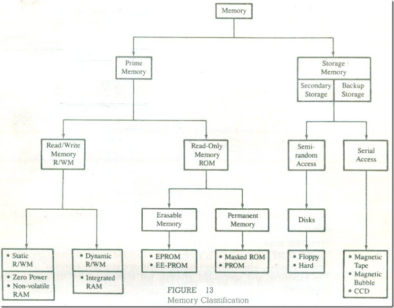
Memory can be classified into two groups: prime(or main) memory and storage memory .The RIWM and ROM discussed in the last section are examples of prime memory; this is the memory the microcomputer uses in executing and storing programs. This memory should be able to respond fast enough to keep up with the execution speed of the microprocessor. Therefore. it should be random-access memory, meaning that the microprocessor should be able to access information from any register with the same speed (independent of its place in the chip).

Storage memory includes examples such as magnetic disks and tapes (see Figure 13). This memory is used to store programs and results after the comple­tion of program execution. Information stored in’ these memories is nonvolatile, meaning information remains intact even if the system is turned off. Generally, these memory devices are not a part of any system; they are made part of the system only when stored programs need to be accessed. The microprocessor can­not execute or directly process programs stored in these devices: programs must be copied into the prime memory first. Therefore, the size of the prime memory (e.g., 64K or 128K) determines how large a program the system can process. The size of the storage memory is unlimited; when one disk or tape is full. Another can be used.

Figure 13 shows two subdivisions of storage memory: secondary storage and backup storage. The secondary storage is similar to what you put on your shelf in your study, and the backup is similar to what you store in your attic. Storage memory includes such devices as disks, magnetic tapes, magnetic. bubble memory, and charged-coupled devices (CCD), The primary features of all these

Memory Classification -16_03

FIGURE 13

Memory Classification

devices are high capacity, low cost, and slow access. A disk is similar to a record; the access to the stored information in the disk is semi-random. The remaining devices shown in Figure 13 are serial: if information is stored in the middle of the tape, it can be accessed only after running half the tape. We will discuss some of these memory storage devices again in Chapter 7. In this chapter, we will focus on various types of prime memory.

Figure 13 shows that the prime memory is divided into two main groups:

Read/Write Memory (R/WM) and Read-Only Memory (ROM), and each group includes several different types of memory.

R/WM (READIWRITE MEMORY)

As the name suggests, the microprocessor can write into or read from this mem­ory, and it is popularly known as Random-Access Memory (RAM). It is used primarily for information that is likely to be altered, such as writing programs or receiving data. This memory is volatile, meaning that when the power is turned off, all its contents are destroyed.

Two types of R/W memories-static and dynamic-are available . Static memory is made of flip-flops ,and it stores the bit as a voltage. Dynamic memory is made MOS transistor gates, and it stores the bit as a charge . the advantage is of the dynamic memory are that it has higher density. Lower power consumption, and is cheaper than the static memory. The disadvantage is that the charge(bit information). therefore, stored information needs to be read and written again every few milliseconds. This is called refreshing the memory ,and it requires extra circuitry, which adds to the cost of the system. It is generally economical to use dynamic memory when the system memory size is larger than 16K; for smaller systems, the static memory is appropriate.

ROM (READ-ONLY MEMORY)

The ROM is a nonvolatile memory; it retains stored information even if the power is turned off. This memory is used for programs and data that need not be altered because, as the name suggests, the information can be read only so that once a bit pattern is stored, it is permanent or at least semi permanent. The permanent group includes two types of memory: masked ROM and PROM, and the semi permanent group also includes two types of memory: EPROM and EE-PROM as shown in Figure 13.

MASKED ROM

In this ROM, a bit pattern is permanently recorded by the masking and metalli­zation process. which memory manufacturers are generally equipped to do. It is an expensive and specialized process, but economical for large production quantities.

PROM (PROGRAMMABLE READ-ONLY MEMORY)

This memory has nichrome or polysilicon wires arranged in a matrix; these wires can be functionally viewed as diodes or fuses. This memory can be programmed by the user with a special PROM programmer that selectively burns the fuses according to the bit pattern to be stored. The process is known a "burning the PROM," and the information stored is permanent.

EPROM (ERASABLE PROGRAMMABLE READ-ONLY MEMORY)

This memory stores a bit by charging the floating gate of a field-effect transistor (FET). Information is stored by using an EPROM programmer .which applies high voltages to charge the gate. All the information can be erased by exposing the chip to ultraviolet light through its quartz window, and the chip can be repro­grammed. Because the chip can be reused many times, this memory is ideally suited for product development, experimental projects, and college laboratories.

EE-PROM (ELECTRICALLY ERASABLE PROM)

This memory is functionally similar to EPROM, except that information can be altered by using electrical signals at the register level rather than erasing all the information. This has an advantage in field and remote control applications. In microprocessor systems, software update is a common occurrence. If EE-PROMs are used in the systems, they can be updated from a central computer by using a remote link via telephone lines. Similarly, in a process control in which timing information has to be changed, it can be done by sending electrical signals from a central place. This memory also includes a chip-erase mode whereby the entire chip can be erased in 10 ms as opposed to 15 to 20 minutes for an EPROM.

RECENT ADVANCES IN MEMORY TECHNOLOGY

Memory technology has advanced considerably in recent years. In addition to static and dynamic R/W memory, there are now more options available in memory devices. Recent examples include Zero Power RAM from MOSTEK, Non-Vola­tile RAM from Intel, and Integrated RAM from several manufacturers.

The Zero Power RAM is a complementary metal-oxide semiconductor (CMOS) Read/Write memory with battery backup built internally. It includes lith­ium cells and voltage-sensing circuitry. When the external power supply voltage falls below + 3 Y, the power switching circuitry connects the lithium battery; thus, this memory provides the advantages of both R/W and Read-Only Memory.

The Non- Volatile RAM is a high speed static R/W Memory array backed lip, bit for bit, by an EE-PROM array for nonvolatile storage. When the power is about to go off, the contents of R/W memory are quickly stored in the EE-PROM by activating a STORE signal on the memory chip, and the stored data can be read into the R/W memory segment when the power is turned on again. This memory chip combines the flexibility of static R/W memory with the novolatility of EE-PROM.

The Integrated RAM (iRAM) is a dynamic memory with the refreshed cir­cuitry built on the chip. For the user. it is similar to the static R/W memory. The user can derive the advantages of the dynamic memory without having to build the external refreshing circuitry. At present, this memory is economical for a sys­tem with medium-sized memory (between 8K and 64K).


Memory Map

Memory Map

Typically, in an 8-bit microprocessor system, 16 address lines are available for memory. This means it is a numbering system of 16 binary bits and is capable of identifying 216 (65,536) memory registers. each register with a 16-bit address. The entire memory addresses can range from 0000 to FFFF in Hex. A memory map is like a pictorial representation in which memory devices are located in the entire range of addresses. Memory addresses provide the locations of various memory devices in the system, and the interfacing logic defines the range of memory ad­dresses for each memory device.

Memory Map -10_13

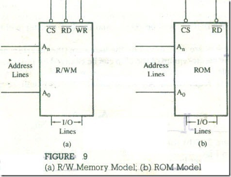
Figure 9

(a) RIW Memory Model; (b) ROM Model

Now let us assume that we have a memory chip with 256 registers that needs only eight address lines (28 = 256). How can we assign 16-bit addresses to 256 registers? This can be accomplished by using the remaining eight lines for the Chip Select through appropriate logic gates as illustrated in the next example.

Example 1

Illustrate the address range of the memory chip with 256 bytes of memory, shown in Figure 10(a), and explain how the address range can be changed by modifying the hardware of the Chip Select CS line in Figure 10(b) .

solution

Figure 10(a) shows a memory chip with 256 registers with 8 I/O lines; the mem­ory size of the chip is Chip Select CS’ signal (active low), and two control signals Read (RD) and write (WR). The eight address line (A7-A0) of the microprocessor are required to iden­tify 256 memory registers. The remaining eight lines (A15-A8) are connected to the chip Select (CS) line through inverters and the NAND gate .The memory chip is enabled or selected when CS goes low. Therefore, to select the chip ,the address lines A15-A8 should be at logic 0,which will cause the output of the NAND gate. to go low .No other logic levels on the lines A Is-AM can select the chip. Once the chip is selected (enabled). the remaining address lines A/An can assume any com­bination from 00H to 00FFH and identify any of the 256 memory registers through .its decoder Therefore, the memory addresses of the chip in Figure 10(a) will range from 0000H to 00FFH as shown below.

Memory Map 11_09

                                                                                                  Chip Enable or Chip Select                                                  Register Select

The address of the first memory register is 0000H, and the address of the last register is 00FFH. If we numbered these registers in decimal with a four-digit sys­tem, the address of the first register will be 000010, and the last register will be 025510.

The chip select addresses are determined by the hardware (the inverters and ‘NAND gate); therefore, the memory map of the chip can be changed by modifying the hardware. For example, if the inverter on line Allis removed as shown in Figure 10(b). the address required on A15-A8 to enable the chip will be follows:

Memory Map 11_13

The memory map for Figure 10(b) will be 8000H to 80FFH·

The memory chips in Figures I0(a) and (b) are the same chips. However by changing the hardware of the Chip Select logic, the location of the memory in the map can be changed ,and memory can be assigned addresses in various lo­cations over the entire range of 0000 to EFFF .

 Memory Map-12_03

Example 2

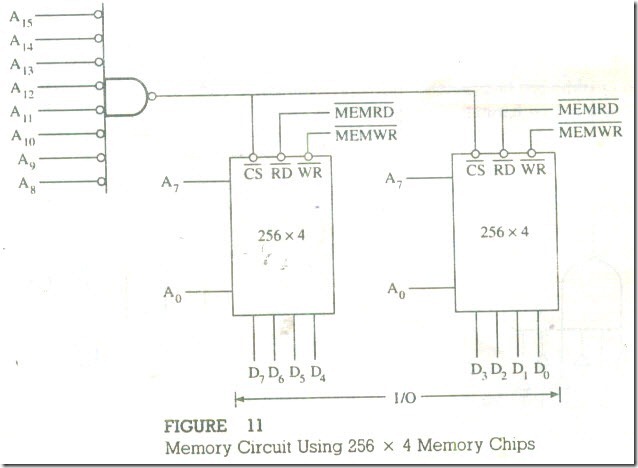
In Figure 10(a), how many 256 x 4 memory chips would be required to replace the 256 x 8 memory chip’? Redraw Figure 10(a) using 256 x 4 memory chips.

solution 

The memory chip with the size of256 x 4 has 256 registers, and each register has four data or 110 lines. Therefore, we would need two 256 x 4 memory chips to replace the 256x 8 memory chip as shown in Figure 11. The address lines A1 to A0 and CS’ line will be the same for both chips; however. data lines D7 to D4 will be connected to the first chip, and the lines D3 to D0 will be connected to the second chip.

In a memory system, a l6-bit address can be conceptually organized into two groups of Hex number .With two Hex digits, 256 registers can be numbered from 00H to FFH as shown in Example 1. This is defined as a page with 256 lines (registers) 10 read from or write on. Similarly ,high-order Hex digits in an address can be used to number the pages from 00H to FFH ; thus, the total range of 64K can be conceptually divided into 256’pages with each page having 256 lines. For example. the memory address 020FH represents line (register) 15 on page 2. and the address 07FFH represents register 255 on page 7. A memory chip with IK (1,024) byte can be viewed as a chip with four pages. This is just a convenient way of thinking about memory addresses.

Memory Map-13_03

Another way of viewing a memory address is in terms of high-order and low order addresses. The lines used for chip select are called high-order address lines, and the lines connected to memory address lines are called low-order address lines. Let us use an example of a four-digit (decimal) numbering system in a high­rise apartment building. Generally, the first two digits (high-order) represent a floor and the last two digits (low-order) represent an apartment number. To locate apartment 1241. we go first to the twelfth floor (similar to Chip Select in memory addressing), and then we look for the apartment 41 (similar to selecting a register). Now let us use the example of an apartment complex. Let us assume the complex is divided into sections I to 9, and each section has up to 999 apartments. In this situation, the number 245) would represent Section 2 and apartment number 451; the digit 2 is a high-order address. and 451 is a low-order address. This is similar to memory addresses of 1 K memory. The I K memory chip will require 10 address lines. and the remaining six lines of the address bus will be used for the CS’. Thus, the group of six address lines will be high order, and the remaining ten address lines will be low order. The memory addresses will be determined by combining the logic levels of these address lines. If the number of address lines in a micro­processor is larger than 16, we will use a five-digit Hex numbering scheme.

Example 3

If the address range of a memory chip is from 4000H to 43FFH, calculate the num­ber of memory registers in the chip.

Solution

The number of registers in Hex: 43FFH – 4000H = 3FFH

The decimal equivalent of 3FFH = 1023

Therefore, the total number of registers in the chip = 1024 (I K). To include the first address, we need to add one to the calculated value.

How the MPU Writes into and Reads from Memory

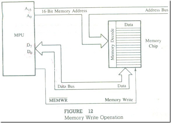
To store (write) a byte into a memory location (Figure 12), the MPU

1. Places the 16-bit address on the address bus of the memory location where a byte is to be stored .The interfacing logic of the memory chip decodes the address and selects the memory register-to be written into.

2. Places the byte on the data bus.

3 . Send the control signal Memory Write to enable the input buffers of the memory and then stores the byte.

To read from memory the steps are similar to that of writing into memory, except the order of steps 2 and 3.

1. The MP places the 16-bit address on the address bus of the memory location from where a byte is to be read. The interfacing logic of the memory chip decodes the address and selects the appropriate memory register.

2. The MPU sends the control signal Memory Read to enable the output buffer of the memory chip.

3. The memory chip places the data byte on the data bus ,and the MPU reads the data byte.

Memory Map15_03

FIGURE 12

Memory Write Operation


MEMORY

MEMORY

Memory is an essential component of a microcomputer system; it stores binary instructions and data for the microprocessor. There are various types of memory, and they can be classified in two groups: prime (or main) memory and storage memory. In the last chapter. we saw two examples of prime memory: Read/Write Memory (R/WM) and Read-Only Memory (ROM). Magnetic tapes and disks can be cited as examples of storage memory. First. we will focus on prime memory and then briefly discuss storage memory when we examine various types of memory.

The R/W memory is made up of registers, and each register has a group of

flip-flops or field-effect transistors that store bits of information. The user can use this memory to hold programs and store data. On the other hand, the ROM stores information permanently in the form of diode ; the group of diodes can be viewed as a register. In a memory chip. all registers are arranged in a sequence and iden­tified by binary numbers called memory addresses. The MPU uses its address bus ­to send the address of a memory register and uses data and control buses to read from or write into that register. In the following sections, we examine the basic concepts related to memory-its structure, its addresses. and its requirements for communication with the MPU-and build a model for RJW memory. However, the discussion is equally applicable to ROM except for slight differences in Read! Write control signals.

Flip-Flop or Latch as a Storage Element

What is memory? It is a circuit that can store bits-generally high or low voltage levels representing 1 and O. A flip-flop or a latch is a basic element of memory.

MEMORY -6_03

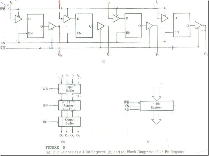
FIGURE 4

Latches as Storage Elements

To write or store a bit in the latch. we need an input data bit and an enable signal (Figure 4(a)) . In this latch, the stored bit is always available on the output line. If a tri-state buffer is connected to the output of the latch(as shown in Figure 4(b) , the stored bit can be read only when the buffer is enabled . Similarly. we can also use a tri-state buffer on the input of the latch. Now we can write into the latch (Figure 4(c)) by enabling the input buffer and read from it by enabling the output buffer. This latch. which can store one binary bit. is called a memory cell. Figure 5(a) shows four such cells or latches grouped together to form a register that has four input lines and four output lines and can store four bits. The size of this register is specified as either 4-bit or 1 x 4 bit which indicates one register with four cells or four I/O lines. The number of bits stored in a register is called a memory word. Figures 5(b) and (c) show simplified block diagrams of the 4- bit register.

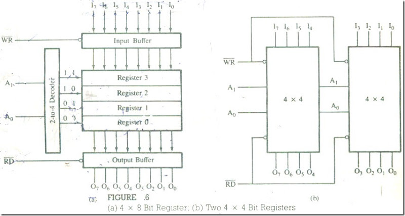
In Figure 6(a), four registers with eight cells (or 8-bit memory word) are arranged in a sequence :to write into or read from anyone of the registers. specific register should be identified or enabled .This is a simple decoding func­tion :a 2-to-4 decoder can perform that function. However. two more input lines A1 and A0, called address lines. are required to the decoder. These two input lines can carry four different bit combinations (00. 01. 10, 11), and each combination can identify or enable one of the registers named as Register 0 through Reg­ister 3.

In Figure 6(a), the chip has an 8-bit memory word, and its size can be specified as 32 bits, 4 x 8 bits, or 4 bytes. If we have a memory chip with a 4-bit memory word, we can combine two such chips in parallel to make an 8-bit mem­ory word as shown in Figure 6(b). The address lines and RD/WR control signals ( -indicates active low) will be connected in parallel, but the memory word will consist of 4 bits from each chip as shown.

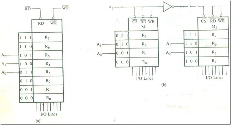
Now we can expand the number of registers. If we have eight registers on one chip, we need three address tines and a 3-to-8 decoder. an interesting problem is how to deal with two chips with four registers each . We have a total of eight registers ; therefore, we need throe address lines. One address line. A,. is used to select a chip, and the address lines A1 and A0 are connected to both chips.

MEMORY -7_03

MEMORY -8_03

FIGURE 6

(a) 4 x 8 Bit Register; (b) Two 4 x 4 Bit Registers

Figure 7(b) shows that the Chip Select signal CS’ is active low .so that when A2 is 0 (low). Chip M1 is selected and when A2 is 1 (high), Chip M2 is selected. The ad­dresses on A1 and An will determine the registers to be selected; thus. by combin­ing the logic on A2. A1. and A0. the memory addresses range from 000 to 111. The concept of the Chip Select signal gives us more flexibility in designing chips and allows us to expand memory size by using multiple chips.

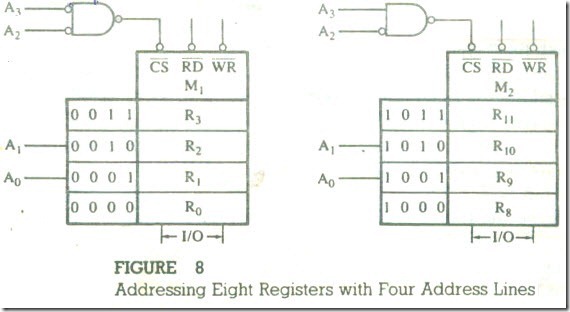
Now let us examine the problem from a different perspective. Assume that we have available four address lines and two memory chips with four registers each as before .Four address lines are capable of identifying sixteen (24) registers: however ,we need only three address lines to identify eight registers .What should we do with the fourth line? One of the solutions is shown in Figure 8. Memory chip M1 is selected when A3 and A2 are both 0; therefore. registers in this chip are identified with the addresses ranging from 0000 to 0011 (0 to 3). Similarly. the addresses of memory chip Ml range from 1000 to 1011 (8 to B); this chip is selected only when A3 is 1 and A2 is 0. In this example. we need three lines to identify eight registers. two for registers and one for Chip Select. However. we used also the fourth line for Chip Select. This is called complete or absolute decoding. An­other option is to leave the fourth line as "don’t care"; we will further explore this concept later.

After reviewing the above explanation, we can summarize the requirements of a memory chip as follows:

memory-9_03

FIGURE 7

(a) Memory Chip with Eight Registers; (b) Two Memory Chips with Four Registers Each

1. A memory chip requires address lines to identify a memory register, a Chip. Select CS’ signal to enable the chip, and control signals to read from and write into memory registers.

2. The number of address lines required is determined by the number of registers in a chip (2n = Number of registers where n is the number of address lines).

3. If additional address lines are available in a system. they are used to enable the Chip Select CS’ signal. The memory address of a register is determined by

memory-9_07

FIGURE 8

Addressing Eight Registers with Four Address Lines

the logic levels (011) of all the address lines (including the address lines used for CS’).

4. The control signal Read (RD’) enables the output buffer. and data from the selected register are made available on the output lines. Similarly, the control signal Write (WR’) enables the input buffer, and data on the input lines are written into memory cells.

A model of a typical memory chip representing the requirements just stated is shown in Figure 9. Figure 9(a) represents the R/W memory and Figure 9(b) represents the Read-Only Memory; the only difference between the two as far as addressing is concerned is that ROM does not need a WR’ signal. Internally, the memory cells are arranged in a matrix format (in rows and columns), because as the size increases the internal decoding scheme we discussed becomes impracti­cal. For example, a memory chip with 1024 registers would require a 10-to-1024 decoder. 1f the cells are arranged in six rows and four columns, however. the internal decoding circuitry can be designed with two decoders, one for-selecting a row and the other for selecting a column. The internal row and column arrangement does not affect our external interfacing logic.


Microprocessor as a Processing Unit

Microprocessor as a Processing Unit

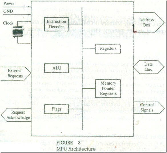
When the microprocessor executes instructions, it does so in a continuous se­quence of fetch, decode, and execute operations. After examining these opera­tions in more detail, we can describe the requirements of the internal architecture of our generalized microprocessor.

FETCHING AN INSTRUCTION

To fetch an instruction, the microprocessor places a memory address on the ad­dress bus and reads binary information using the data bus .Therefore, it needs a register that can hold memory addresses and increment these addresses after the fetching is completed, a sort of memory pointer.

DECODING AN INSTRUCTION

Once an instruction byte is fetched,’ it needs to be decoded to answer the following:

· Is it a complete instruction? If not, how many more bytes need to be fetched?

· What type of operation is required and on what data ?

To perform these functions. the microprocessor needs an instruction decoder that can interpret the fetched binary information.

STORING DATA

The microprocessor gets data from memory, I/O, or directly as part of an instruction. Therefore. it needs a set of registers to store data (or addresses) temporarily before it can process the data.

EXECUTING AN INSTRUCTION

The type of data manipulation the microprocessor can perform depends on its internal micro programs , that is, on its instruction SCI. These operations can be classified as data copy (transfer). arithmetic/logic operations, and decision mak­ing .For example. to subtract two numbers, both numbers must be loaded into registers. After the subtraction, it is necessary to indicate whether the result is positive, negative, or zero. This can be indicated by setting or resetting flip-flops called flags. To perform these arithmetic and logic operations. the microprocessor needs a group of logic circuits called Arithmetic/Logic Unit (ALU).

This description of the requirements of the microprocessor to process data

Microprocessor as a Processing Unit _03

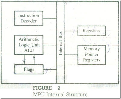
FIGURE 2

MPU Internal Structure

can be summarized in a simplified block diagram shown in Figure 2 From this block diagram, we can derive a programming model for a specific microprocessor.

Review of Important Concepts

The description and the requirements of a generalized microprocessor unit can be summarized as follows

Microprocessor as a Processing Unit -4_06

FIGURE 3

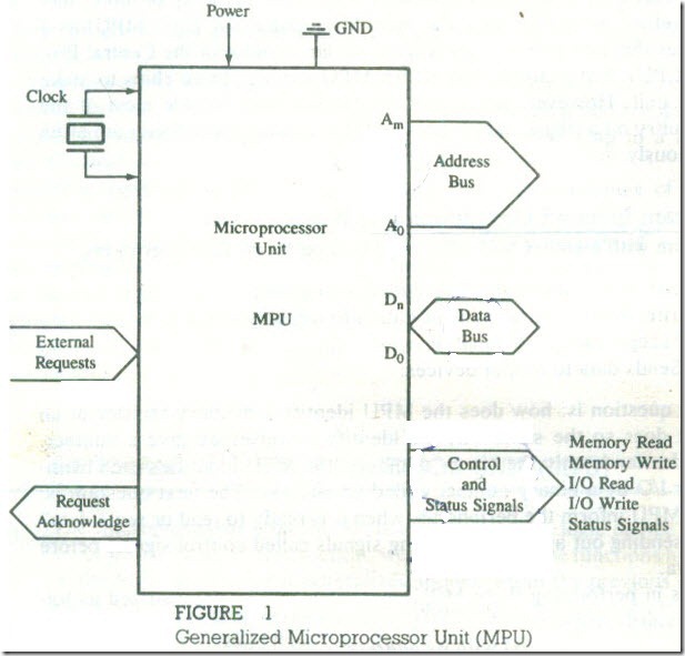
To communicate with memory and I/O devices, the MPU should have the following:

l. Address bus to send the address of a memory register or an I/O.

2. Data bus to transfer data between the MPU and memory and I/O devices.

3. Control signals to identify its operations and provide timing .

4. External Request signal lines to interrupt the MPU operations.

5. Request Acknowledge signals to respond to the requests by peripherals.

6. Clock signal to provide timing and power to operate circuits.

To process data internally, the MPU should include the following:

1. Instruction Decoder to decode the fetched binary information.

2. Registers to store binary data.

3. Registers as memory pointers for addressing memory registers.

4. ALU to perform arithmetic and logic operations.

5. Flags (flip-flops) to indicate data conditions for decision making.


Microprocessor ­Based System : MPU, Memory, and 1/0

Microprocessor ­Based System : MPU, Memory, and 1/0

A microprocessor-based system consists pri­marily of three components-the micropro­cessor unit (MPU). memory. and I/O (input / output). The MPU is the central player; it com­municates with memory and I/O devices. pro­cesses data, and controls timing of all its oper­ations. In this chapter. we will examine what the MPU does and what its requirements are. We then design a model for a generalized MPU that expands on the bus concept discussed in the previous chapter and shows signals neces­sary for the MPU to communicate with other devices. The model also describes the require­ments for processing data and shows registers and logic circuits the MPU needs.

Memory and 1I0s are integral parts of a microprocessor-based system. We will discuss memory in terms of its basic elements-latches and registers-and specify the requirements for a memory chip to store information and com­municate with the MPU. Based on those re­quirements, we then develop the concepts of memory addressing and memory maps. We also discuss how the MPU addresses and commu­nicates with I/Os.

OBJECTIVES

· List the four program-initiated operations performed by the MPU.

· Define the functions of the address bus. data bus. and control signals.

· List the externally initiated operations the MPU should respond to.

· Draw the model of a generalized MPU show­ing the necessary signals.

· List the types of registers the MPU needs to process data internally.

· Explain the internal organization of memory and the requirements of a memory chip to store information and communicate with the MPU.

· Explain the functions of the control signals: Chip Select (CS). Read (RD),and Write (WR).

· Explain how memory addresses are assigned to a memory chip and recognize the’ address range of a given chip in a microprocessor ­based system.

· List the two techniques of addressing I/O devices.

· Draw a block diagram of a microprocessor based system showing the MPU. memory. I/Os. and buses.

The Microprocessor Unit (MPU)

is a programmable logic device with a designed set of instructions. In this section. we will examine the functions and requirements of the MPU and derive a generalized model. From the previous chapter, we can recall what the MPU does. It reads or fetches each instruction, one at a time, from memory and performs data manipulation specified by the instruction; it also reads data from input devices. and writes (or sends) data to output devices.

When the MPU is executing a program. it communicates frequently with memory and 1/0 devices; the process consists of fetch, decode, and execute op­erations. However. the question is: Can it respond to unexpected events? For example, while printing a long program. can it stop printing temporarily and read any critical data that may arrive at the input? Can it be "interrupted"? Can it wait until a peripheral is ready? For example. when memory response is too slow, can the MPU wait until memory is ready? The answer to all these questions must be affirmative.

In addition to processing data according to the instructions written in memory, the MPU needs to respond to various situations described above. External devices should be able to interrupt and request the attention of the MPU. This communication process and related operations between the MPU and the external devices (memory, 1/Os) can be classified into two main categories:

· Program-initiated operations

· Peripheral (or externally) initiated operations.

To perform these operations, the MPU requires a group of logic circuits, a set of signals to transfer information, control signals for timing, and clock cir­cuitry; these constitute the architecture. Early microprocessors did not have the necessary circuitry on one chip; the complete units were made up of more than one chip. Therefore, we define here the term Microprocessor Unit (MPU) as a group of device that can perform operations similar to those of the Central Pro­cessing Unit (CPU). For example, the 8080A MPU requires three chips to make it a functional unit. However, since later microprocessors include most of the necessary circuitry on a single chip, the terms MPU and microprocessor are often used synonymously.

Program-Initiated Operations and Buses 

To communicate with memory and IIOs, the MPU performs four operations:

1. Memory Read: Reads instructions or data from memory.

2. Memory Write: Writes instructions or data into memory.

3. I/O Read: Accepts data from input devices.

4. I/O Write: Sends data to output devices.

Now the question is: how does the MPU identify a memory register or an I/O device? It does so the same way we identify a house: we give a number. Because it understands only the binary numbers, the MPU identifies each mem­ory register or 1/0 by a binary number called an address. The next question is: how does’ the MPU inform the peripherals when it is ready to read or write data? It does so by sending out appropriate timing signals called control signals before it transfers data.

The steps in performing these MPU operations can be summarized as fol­lows (not necessarily in the order listed in every operation):

1. Identify the memory location or the peripheral with its address.

2. Provide timing or synchronization signal.

3. Transfer binary data.

Therefore, the MPU requires three sets of communication lines called buses: the first group of lines, called the address bus, to identify the memory loca­tion; the second group, called the data bus, to transfer data; and the third group, called the control lines, for timing signals. In the previous chapter (Figure 1.3), all these different signal lines were grouped together and shown as the system bus. Now we. shall describe them individually.

ADDRESSBUS

As mentioned earlier, the MPU identifies each peripheral or memory location with a binary address. Now the question is: how large is this address? The answer depends upon the internal design of the microprocessor and available pins on a chip; it can be eight, 16, 20, or more bits. If the address size is 4 bits, the micro­processor can identify 16 (24) different memory locations. The addressing is sim­ply a numbering scheme to identify memory registers. For example, a two-digit decimal numbering scheme can identify only 100 items, from 00 to 99. On the other hand, a four-digit numbering scheme can identify 10,000 items, from 0000

to 9999. Thus, the number of bits (address lines) used for addressing by the MPU clearly determines the number of memory registers it can identify.

Microprocessor ­Based System  MPU, Memory, and 10

FIGURE 1 Generalized Microprocessor Unit (MPU)

Figure 1  shows one group of lines as the address bus for our generalized MPU. The arrow suggests that these lines are unidirectional-the signals flow . from the MPU to peripherals because only the MPU sends out an address. The address lines are generally identified as A0 to Am where m indicates the most significant address bit. Typically, earlier microprocessors such as the 8085. the Z80, and the 6800 have 16 address lines which are capable of addressing 65.5 ‘0 (2Ih) memory locations, commonly known as 64K memory. However, recent microprocessors such as the 8086 have 20 address lines, and the 68000 has 23 address lines.

DATA BUS

The second group of lines shown in Figure 2 is the data bus. These lines are used to transfer data and are bidirectional-data can flow either direction. These lines are identified as D0 to Dn where n signifies the most significant bit (MSB) of the data bus. Again, the size of the data bus determines how large a binary ­number can be transferred and processed at a time and thus influences the microprocessor architecture considerably. The 8085, the Z80, and the 6800 have eight data lines and thus are called S-bit microprocessors .On the other hand. the 8086. the 80286, the Z8oo0. and the 68000 have 16 data lines and are called 16-bit microprocessors.

CONTROL SIGNALS (MPU INITIATED)

These are individual signal lines generated by the MPU to indicate its operations. The MPU generates a specific signal for each of its four operations-Memory Read. Memory Write, 1/0 Read, and I/O Write. These are timing signals that are used to enable, or activate, peripherals. For example, to fetch (or read) an instruction from a memory location, the MPU sends a timing pulse called Memory Read to enable the memory chip.

Externally Initiated Operations

There are various occasions when ongoing MPU operations need to be inter­rupted. For the MPU we are designing, we can classify these types of external interruptions or delays into four categories.

· Reset: Start again from the beginning. For example, if we are using a micropro­cessor as a timer, we should be able to reset the timer after each operation or in the middle of an operation and start again.

· Interrupt: Stop the ongoing process temporarily; do something now that is more critical, and then go back to the original process. For example. we should be able to stop printing temporarily and read data from a keyboard; then. when the MPU finishes reading that data, it can go back to printing.

· Wait: When memory response time is too slow to respond to the speed of the MPU, this signal can be used to delay the MPU operations.

· Bus Request: When the MPU operations are too slow compared to the speed of a peripheral, the peripheral can request the use of the buses. For example. when large amounts of data are to be transferred to memory, Direct Memory Access (DMA) controllers can transfer data much faster than can the MPU.

In our generalized MPU model (Figure 2). these externally initiated signals are shown as External Requests. To indicate its response to some of these ex­ternal requests, the MPU needs additional signal lines shown as Request Acknowledge.

Clock Signals and Power

The MPU can be viewed as a complex timer. The timing is very critical in all its operations. The bits of a binary instruction are associated with the micro programs inside the chip; when the MPU executes an instruction, it releases a series of micro programs at precise rime intervals. Therefore, the MPU needs circuits that generate clock signals. In addition, it needs electrical power to run all the operations.

Figure 1 shows all the signals necessary for our generalized MPU. Pres­ently, because of LSI technology, most of the MPU requirements can be satisfied by single-chip microprocessors with slight variations. For example, the Z80 mi­croprocessor has all the signals of the MPU except c1ock-generatlng circuitry. and some of its control signals need to be logically ANDed to generate the specific control signals shown in Figure 8 However. the present microprocessors in­clude all the data processing and timing circuitry on one chip; therefore, they can be viewed almost as MPUs. Now we shall examine what is inside the microprocessor to understand how it processes data.


SUMMARY Of Microprocessors, Microcomputers, and Assembly Language

SUMMARY

The various concepts and terms discussed in this chapter are summarized below:

Computer Structure

· Digital Computer-a programmable machine that processes binary data. It includes four components: CPU (ALU plus control unit), memory, input, and output.

· CPU-the Central Processing Unit. The group of circuits that processes data and provides control signals and timing. It includes the arithmetic/logic unit, registers, instruction decoder, and the control unit.

· ALU-the group of circuits that performs arithmetic and logic operations. The ALU is a part of the CPU.

· Control Unit-The group of circuits that provides timing and signals to all operations in the computer and controls data flow.

· Memory-a medium that stores binary information (instructions and data).

· Input -a device that transfers information from the outside world to the computer.

· Output-a device that transfers information from the computer to the outside world.

Scale of Integration

· SSI-Small-Scale Integration. The process of designing a few circuits on a single chip. The term refers to the technology used to fabricate discrete logic gates on a chip.

· MSI-Medium-Scalc Integration. The process of designing more than 100 gates on a single chip.

· LSI-Large-Scale Integration. The process of designing more than 1 ,000 gates on a single chip. Similarly, the terms VLSI (Very-Large-Scale Integration) and SLSI (Super-Large-Scale Integration) are used to indicate the scale of integration.

Microprocessor-Based Systems

· Microprocessor-a semiconductor device (integrated circuit) that is manufac­tured by using the large-scale integration technique. It includes the ALU, reg­ister arrays, and control circuits on a single chip.

· Microcomputer-a computer that uses a microprocessor as its CPU. It in­cludes four components: microprocessor, memory, input, and output.

· Bus—a group of lines used to transfer bits between the microprocessor and other components of the computer system.

· ROM-Read-Only Memory. A memory that stores binary information perma­nently. The information can be read from this memory but cannot be altered.

· R/WM-Read/Write Memory. A memory that stores binary information dur­ing the operation of the computer. This memory is used as a writing pad to write user programs and data. The information stored in this memory can be easily read and altered.

Computer Languages

· Bit-A binary digit, 0 or 1.

· Byte-a group of eight bits.

· Nibble-a group of four bits.

· Word-a group of bits the computer recognizes and processes as a whole.

· Instruction-a command in binary that is recognized and executed by the computer in order to accomplish a task. Some instructions are designed with one word, and some require multiple words.

· Mnemonic-a combination of letters to suggest the operation of an instruc­tion.

· Program-a set of instructions written in a specific sequence for the computer to accomplish a given task.

· Machine Language-the binary medium of communication with a computer through a designed set of instructions specific to each computer.

· Assembly Language-a medium of communication with a computer in which programs are written in mnemonics. An assembly language is specific to a given computer.

· Low-Level Language-a medium of communication that is machine-depen­dent, or specific to a given computer. The machine and the assembly lan­guages of a computer are considered low-level languages. Programs written in these languages are not transferable to different types of machines.

· High-Level Language-a medium of communication independent of a given computer. Programs are written in English-like words, and they can be exe­cuted on a machine using a translator (a compiler or an interpreter).

· Compiler-a program that translates English-like words of a ‘high-level language into the machine language of a computer. A compiler reads a given pro­gram, called a source code, in its entirety, and then translates the program into the machine language, which is called an object code.

· Interpreter-a program that translates the English-like statements of a high ­level language into the machine language of a computer. An interpreter trans­lates one statement at a time from a source code to an object code.

· Assembler-a computer program that translates an assembly language pro­gram from mnemonics to the binary machine code of a computer.

· Hand Assembly-a procedure of looking up the machine code manually from the instruction set of a microprocessor and entering those codes into the com­puter through a keyboard.

· Monitor Program-a program that interprets the input from a keyboard an converts the inputinto its binary equivalent.

LOOKING AHEAD

This chapter has given a brief introduction to computer organization and com­puter languages, with emphasis on the Z80 microprocessor and its assembly lan­guage. The chapter has given an overview of the entire spectrum of computers, including their salient features and applications. The primary focus ‘of this book is on the architectural details of the Z80 microprocessor and its industrial appli­cations. and on assembly language programming in the context of these applica­tions. In the microcomputer field, there is hardly any separation between hard­ware and software. especially in applications where assembly language is necessary. In designing a microprocessor-based product, hardware and software tasks are carried out concurrently because a decision in one area affects the planning of the other area. There are various functions that can be performed through either hardware or software. and a designer needs to consider both ap­proaches. This book focuses on trade-off between the two approaches as a design philosophy.

ASSIGNMENTS

1. List the components of a microprocessor-based system or a computer.

2. Explain the functions of each component of a computer.

3. What is a microprocessor? What is the difference between a microprocessor and a CPU?

4. Explain the difference between a microprocessor and a microcomputer.

5. Explain the following terms: SSI. MSI. and LSI.

6. Define: bit. byte, word, and instruction.

7. How many bytes make a word of 32 bits?

8. Explain the difference between the machine language and the assembly lan­guage of the Z80 microprocessor.

9. What is an assembler?

10. What are low- and high-level languages?

11. Explain the difference between a compiler and an interpreter.

12. What are the advantages of an assembly language in comparison with high ­level languages?