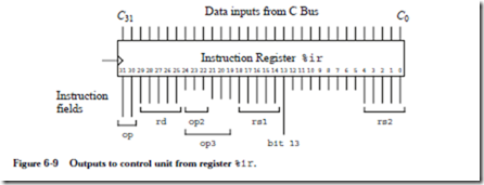
Memory: chip organization (constructing large rams from small rams) and commercial memory modules.

7.1 Chip Organization

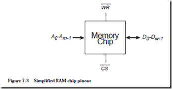
A simplified pinout of a RAM chip is shown in Figure 7-3. An m-bit address,

image

having lines numbered from 0 to m-1 is applied to pins A0-Am-1, while asserting CS (Chip Select), and either WR (for writing data to the chip) or WR (for reading data from the chip). The over bars on CS and WR indicate that the chip is selected when CS=0 and that a write operation will occur when WR=0. When reading data from the chip, after a time period tAA (the time delay from when the address lines are made valid to the time the data is available at the output), the w-bit data word appears on the data lines D0Dw-1. When writing data to a chip, the data lines must also be held valid for a time period tAA. Notice that the data lines are bidirectional in Figure 7-3, which is normally the case.

The address lines A0- Am-1 in the RAM chip shown in Figure 7-3 contain an address, which is decoded from an m-bit address into one of 2m locations within the chip, each of which has a w-bit word associated with it. The chip thus contains 2m´w bits.

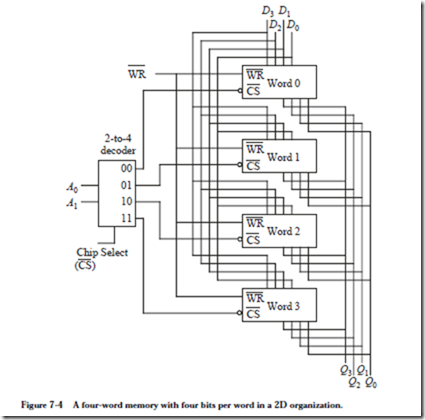
Now consider the problem of creating a RAM that stores four four-bit words. A RAM can be thought of as a collection of registers. We can use four-bit registers to store the words, and then introduce an addressing mechanism that allows one of the words to be selected for reading or for writing. Figure 7-4 shows a design

image

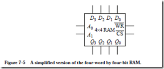
for the memory. Two address lines A0 and A1 select a word for reading or writing via the 2-to-4 decoder. The outputs of the registers can be safely tied together without risking an electrical short because the 2-to-4 decoder ensures that at most one register is enabled at a time, and the disabled registers are electrically disconnected through the use of tri-state buffers. The Chip Select line in the decoder is not necessary, but will be used later in constructing larger RAMs. A simplified drawing of the RAM is shown in Figure 7-5 .

There are two common ways to organize the generalized RAM shown in Figure 7-3. In the smallest RAM chips it is practical to use a single decoder to select one

image

out of 2m words, each of which is w bits wide. However, this organization is not economical in ordinary RAM chips. Consider that a 64M´1 chip has 26 address lines (64M = 226). This means that a conventional decoder would need 226 26-input AND gates, which manifests itself as a large cost in terms of chip area – and this is just for the decode.

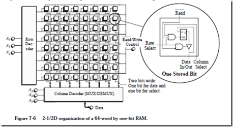
Since most ICs are roughly square, an alternate decoding structure that significantly reduces the decoder complexity decodes the rows separately from the columns. This is referred to as a 2-1/2D organization. The 2-1/2D organization is by far the most prevalent organization for RAM ICs. Figure 7-6 shows a 26-word

image

x1-bit RAM with a 2 1/2D organization. The six address lines are evenly split between a row decoder and a column decoder (the column decoder is actually a MUX/DEMUX combination). A single bidirectional data line is used for input and output.

During a read operation, an entire row is selected and fed into the column MUX, which selects a single bit for output. During a write operation, the single bit to be written is distributed by the DEMUX to the target column, while the row decoder selects the proper row to be written.

In practice, to reduce pin count, there are generally only m/2 address pins on the chip, and the row and column addresses are time-multiplexed on these m/2 address lines. First, the m/2-bit row address is applied along with a row address strobe, RAS, signal. The row address is latched and decoded by the chip. Then the m/2-bit column address is applied, along with a column address strobe, CAS. There may be additional pins to control the chip refresh and other memory functions.

Even with this 2-1/2D organization and splitting the address into row and col- umn components, there is still a great fanin/fanout demand on the decoder logic gates, and the (still) large number of address pins forces memory chips into large footprints on printed circuit boards (PCBs). In order to reduce the fanin/fanout constraints, tree decoders may be used, which are discussed in Section 7.8.1. A newer memory architecture that serializes the address lines onto a single input pin is discussed in Section 7.9.

Although DRAMs are very economical, SRAMs offer greater speed. The refresh cycles, error detection circuitry, and the low operating powers of DRAMs create a speed difference that is roughly 1/4 of SRAM speed, but SRAMs also incur a significant cost.

The performance of both types of memory (SRAM and DRAM) can be improved. Normally a number of words constituting a block will be accessed in succession. In this situation, memory accesses can be interleaved so that while one memory is accessing address Am, other memories are accessing Am+1, Am+2, Am+3 etc. In this way the access time for each word can appear to be many times faster.

7.3.1 CONSTRUCTING LARGE RAMS FROM SMALL RAMS

We can construct larger RAM modules from smaller RAM modules. Both the word size and the number of words per module can be increased. For example, eight 16M ´ 1-bit RAM modules can be combined to make a 16M ´ 8-bit RAM module, and 32 16M ´ 1-bit RAM modules can be combined to make a 64M ´ 8-bit RAM module.

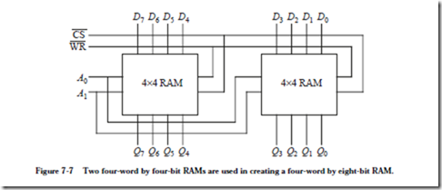
As a simple example, consider using the 4 word ´ 4-bit RAM chip shown in Figure 7-5, as a building block to first make a 4-word ´ 8-bit module, and then an 8-word ´ 4-bit module. We would like to increase the width of the four-bit words and also increase the number of words. Consider first the problem of increasing the word width from four bits to eight. We can accomplish this by simply using two chips, tying their CS (chip select) lines together so they are both selected together, and juxtaposing their data lines, as shown in Figure 7-7.

image

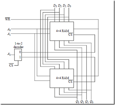
Consider now the problem of increasing the number of words from four to eight. Figure 7-8 shows a configuration that accomplishes this. The eight words are distributed over the two four-word RAMs. Address line A2 is needed because there are now eight words to be addressed. A decoder for A2 enables either the upper or lower memory module by using the CS lines, and then the remaining address lines (A0 and A1) are decoded within the enabled module. A combination of these two approaches can be used to scale both the word size and number of words to arbitrary sizes.

7.4 Commercial Memory Modules

Commercially available memory chips are commonly organized into standard configurations. Figure 7-9 (Texas Instruments, 1991) shows an organization of eight 220-bit chips on a single-in-line memory module (SIMM) that form a 220 ´ 8 (1MB) module. The electrical contacts (numbered 1 – 30) all lie in a single line. For 220 memory locations we need 20 address lines, but only 10 address lines (A0 – A9) are provided. The 10-bit addresses for the row and column are loaded separately, and the Column Address Strobe and Row Address Strobe signals are applied after the corresponding portion of the address is made available. Although this organization appears to double the time it takes to access any par-

image

ticular memory location, on average, the access time is much better since only the row or column address needs to be updated.

The eight data bits on lines DQ1 – DQ8 form a byte that is read or written in parallel. In order to form a 32-bit word, four SIMM modules are needed. As with the other “active low” signals, the Write Enable line has a bar over the corresponding symbol ( W ) which means that a write takes place when a 0 is placed on this line. A read takes place otherwise. The RAS line also causes a refresh operation, which must be performed at least every 8 ms to restore the charges on the capacitors.


MEMORY:The Memory Hierarchy and Random Access Memory.

MEMORY

In the past few decades, CPU processing speed as measured by the number of instructions executed per second has doubled every 18 months, for the same price. Computer memory has experienced a similar increase along a different dimension, quadrupling in size every 36 months, for the same price. Memory speed, however, has only increased at a rate of less than 10% per year. Thus, while processing speed increases at the same rate that memory size increases, the gap between the speed of the processor and the speed of memory also increases.

As the gap between processor and memory speeds grows, architectural solutions help bridge the gap. A typical computer contains several types of memory, ranging from fast, expensive internal registers (see Appendix A), to slow, inexpensive removable disks. The interplay between these different types of memory is exploited so that a computer behaves as if it has a single, large, fast memory, when in fact it contains a range of memory types that operate in a highly coordinated fashion. We begin the chapter with a high-level discussion of how these different memories are organized, in what is referred to as the memory hierarchy.

7.1 The Memory Hierarchy

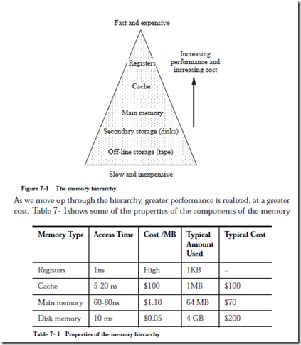
Memory in a conventional digital computer is organized in a hierarchy as illustrated in Figure 7-1. At the top of the hierarchy are registers that are matched in speed to the CPU, but tend to be large and consume a significant amount of power. There are normally only a small number of registers in a processor, on the order of a few hundred or less. At the bottom of the hierarchy are secondary and off-line storage memories such as hard magnetic disks and magnetic tapes, in which the cost per stored bit is small in terms of money and electrical power, but the access time is very long when compared with registers. Between the registers and secondary storage are a number of other forms of memory that bridge the gap between the two.

image

hierarchy in the late 1990’s. Notice that Typical Cost, arrived at by multiplying Cost/MB ´ Typical Amount Used (in which “MB” is a unit of megabytes), is approximately the same for each member of the hierarchy. Notice also that access times vary by approximately factors of 10 except for disks, which have access times 100,000 times slower than main memory. This large mismatch has an important influence on how the operating system handles the movement of blocks of data between disks and main memory, as we will see later in the chapter.

7.2 Random Access Memory

In this section, we look at the structure and function of random access memory (RAM). In this context the term “random” means that any memory location can be accessed in the same amount of time, regardless of its position in the memory.

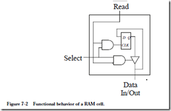
Figure 7-2 shows the functional behavior of a RAM cell used in a typical com-

image

puter. The figure represents the memory element as a D flip-flop, with additional controls to allow the cell to be selected, read, and written. There is a (bidirectional) data line for data input and output. We will use cells similar to the one shown in the figure when we discuss RAM chips. Note that this illustration does not necessarily represent the actual physical implementation, but only its functional behavior. There are many ways to implement a memory cell.

RAM chips that are based upon flip-flops, as in Figure 7-2, are referred to as static RAM (SRAM), chips, because the contents of each location persist as long as power is applied to the chips. Dynamic RAM chips, referred to as DRAMs, employ a capacitor, which stores a minute amount of electric charge, in which the charge level represents a 1 or a 0. Capacitors are much smaller than flip-flops, and so a capacitor based DRAM can hold much more information in the same area than an SRAM. Since the charges on the capacitors dissipate with time, the charge in the capacitor storage cells in DRAMs must be restored, or refreshed frequently.

DRAMs are susceptible to premature discharging as a result of interactions with naturally occurring gamma rays. This is a statistically rare event, and a system may run for days before an error occurs. For this reason, early personal computers (PCs) did not use error detection circuitry, since PCs would be turned off at the end of the day, and so undetected errors would not accumulate. This helped to keep the prices of PCs competitive. With the drastic reduction in DRAM prices and the increased uptimes of PCs operating as automated teller machines (ATMs) and network file servers (NFSs), error detection circuitry is now commonplace in PCs.

In the next section we explore how RAM cells are organized into chips.


Summary of data path and control.

■ SUMMARY

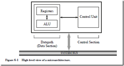
A microarchitecture consists of a data path and a control section. The data path contains data registers, an ALU, and the connections among them. The control section contains registers for microinstructions (for a microprogramming approach) and for condition codes, and a controller. The controller can be micro- programmed or hardwired. A micro programmed controller interprets microinstructions by executing a micro program that is stored in a control store. A hardwired controller is organized as a collection of flip-flops that maintain state information, and combinational logic that implements transitions among the states.

The hardwired approach is fast, and consumes a small amount of hardware in comparison with the micro programmed approach. The micro programmed approach is flexible, and simplifies the process of modifying the instruction set. The control store consumes a significant amount of hardware, which can be reduced to a degree through the use of nanoprogramming. Nanoprogramming adds delay to the microinstruction execution time. The choice of micro programmed or hard- wired control thus involves trade-offs: the micro programmed approach is large and slow, but is flexible and lends itself to simple implementations, whereas the hardwired approach is small and fast, but is difficult to modify, and typically results in more complicated implementations.

■ FURTHER READING

(Wilkes, 1958) is a classic reference on microprogramming. (Mudge, 1978) cov- ers microprogramming on the DEC PDP 11/60. (Tanenbaum, 1990) and (Mano, 1991) provide instructional examples of micro programmed architec- tures. (Hill and Peterson, 1987) gives a tutorial treatment of the AHPL hardware description language, and hardwired control in general. (Lipsett et. al., 1989) and (Navabi, 1993) describe the commercial VHDL hardware description language and provide examples of its use. (Gajski, 1988) covers various aspects of silicon compilation.

Gajski, D., Silicon Compilation, Addison Wesley, (1988).

Hill, F. J. and G. R. Peterson, Digital Systems: Hardware Organization and Design, 3/e, John Wiley & Sons, (1987).

Lipsett, R., C. Schaefer, and C. Ussery, VHDL: Hardware Description and Design, Kluwer Academic Publishers, (1989).

Mano, M., Digital Design, 2/e, Prentice Hall, (1991).

Mudge, J. Craig, Design Decisions for the PDP11/60 Mid-Range Minicomputer, in Computer Engineering, A DEC View of Hardware Systems Design, Digital Press, Bedford MA, (1978).

Navabi, Z., VHDL: Analysis and Modeling of Digital Systems, McGraw Hill, (1993).

Tanenbaum, A., Structured Computer Organization, 3/e, Prentice Hall, Engle- wood Cliffs, New Jersey, (1990).

Wilkes, M. V., W. Redwick, and D. Wheeler, “The Design of a Control Unit of an Electronic Digital Computer,” Proc. IRE, vol. 105, p. 21, (1958).

■ PROBLEMS

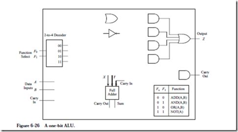
6.1 Design a 1-bit arithmetic logic unit (ALU) using the circuit shown in Figure 6-26 that performs bitwise addition, AND, OR, and NOT on the 1-bit inputs A and B. A 1-bit output Z is produced for each operation, and a carry is also produced for the case of addition. The carry is zero for AND, OR, and

image

NOT. Design the 1-bit ALU using the components shown in the diagram. Just draw the connections among the components. Do not add any logic gates, MUXes, or anything else. Note: The Full Adder takes two one-bit inputs (X and Y) and a Carry In, and produces a Sum and a Carry Out.

6.2 Design an ALU that takes two 8-bit operands X and Y and produces an 8-bit output Z. There is also a two-bit control input C in which 00 selects log- ical AND, 01 selects OR, 10 selects NOR, and 11 selects XOR. In designing your ALU, follow this procedure: (1) draw a block diagram of eight 1-bit ALUs that each accept a single bit from X and Y and both control bits, and produce the corresponding single-bit output for Z; (2) create a truth table that describes a 1-bit ALU; (3) design one of the 1-bit ALUs using an 8-to-1 MUX.

6.3 Design a control unit for a simple hand-held video game in which a character on the display catches objects. Treat this as an FSM problem, in which you only show the state transition diagram. Do not show a circuit. The input to the control unit is a two-bit vector in which 00 means “Move Left,” 01 means “Move Right,” 10 means “Do Not Move,” and 11 means “Halt.” The output Z is 11 if the machine is halted, and is 00, 01, or 10 otherwise, corresponding to the input patterns. Once the machine is halted, it must remain in the halted state indefinitely.

6.4 In Figure 6-3, there is no line from the output of the C Decoder to %r0.

Why is this the case?

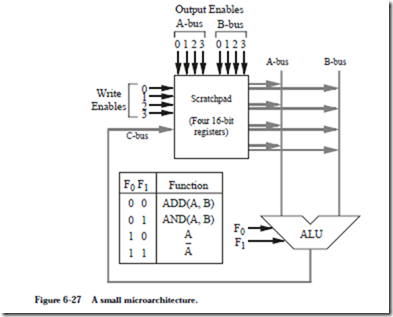
6.5 Refer to diagram Figure 6-27. Registers 0, 1, and 2 are general purpose

image

registers. Register 3 is initialized to the value +1, which can be changed by the microcode, but you must make certain that it does not get changed.

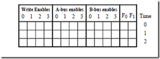
a) Write a control sequence that forms the two’s complement difference of the contents of registers 0 and 1, leaving the result in register 0. Symbolically, this might be written as: r0 ¬ r0 – r1. Do not change any registers except r0 and r1 (if needed). Fill in the table shown below with 0’s or 1’s (use 0’s when the choice of 0 or 1 does not matter) as appropriate. Assume that when no registers are selected for the A-bus or the B-bus, that the bus takes on a value of 0.

image

b) Write a control sequence that forms the exclusive-OR of the contents of registers 0 and 1, leaving the result in register 0. Symbolically, this might be written as: r0 ¬ XOR(r0, r1). Use the same style of solution as for part (a).

6.6 Write the binary form for the microinstructions shown below. Use the style shown in Figure 6-17. Use the value 0 for any fields that are not needed.

image

6.7 Three binary words are shown below, each of which can be interpreted as a microinstruction. Write the mnemonic version of the binary words using the micro-assembly language introduced in this chapter.

image

6.8 Rewrite the microcode for the call instruction starting at line 1280 so that only 3 lines of microcode are used instead of 4. Use the LSHIFT2 operation once instead of using ADD twice.

6.9 (a) How many microinstructions are executed in interpreting the subcc instruction that was introduced in the first Example section? Write the numbers of the microinstructions in the order they are executed, starting with microinstruction 0.

(b) Using the hardwired approach for the ARC microcontroller, how many states are visited in interpreting the addcc instruction? Write the states in the order they are executed, starting with state 0.

6.10 (a) List the microinstructions that are executed in interpreting the ba instruction.

(b) List the states (Figure 6-22) that are visited in interpreting the ba instruction.

6.11 Register %r0 can be designed using only tri-state buffers. Show this design.

6.12 What bit pattern should be placed in the C field of a microword if none of the registers are to be changed?

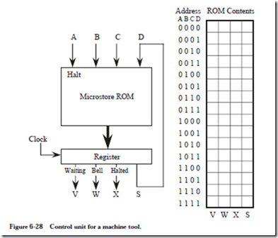
6.13 A control unit for a machine tool is shown in Figure 6-28. You are to cre-

image

ate the microcode for this machine. The behavior of the machine is as follows: If the Halt input A is ever set to 1, then the output of the machine stays halted forever and outputs a perpetual 1 on the X line, and 0 on the V and W lines. A waiting light (output V) is enabled (set to 1) when no inputs are enabled. That is, V is lit when the A, B, and C inputs are 0, and the machine is not halted. A bell is sounded (W=1) on every input event (B=1 and/or C=1) except when the machine is halted. Input D and output S can be used for state information for your microcode. Use 0’s for any fields that do not matter. Hint: Fill in the lower half of the table first.

6.14 For this problem, you are to extend the ARC instruction set to include a new instruction by modifying the microprogram. The new ARC instruction to be microcoded is:

xorcc — Perform an exclusive OR on the operands, and set the condition codes accordingly. This is an Arithmetic format instruction. The op3 field is 010011.

Show the new microinstructions that will be added for xorcc.

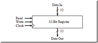
6.15 Show a design for a four-word register stack, using 32-bit registers of the form shown below:

image

Four registers are stacked so that the output of the top register is the input to the second register, which outputs to the input of the third, which outputs to the input of the fourth. The input to the stack goes into the top register, and the output of the stack is taken from the output of the top register (not the bottom register). There are two additional control lines, push and pop, which cause data to be pushed onto the stack or popped off the stack, respectively, when the corresponding line is 1. If neither line is 1, or if both lines are 1, then the stack is unchanged.

6.16 In line 1792 of the ARC microprogram, the conditional GOTO appears at the end of the line, but in line 8 it appears at the beginning. Does the position of the GOTO within a micro-assembly line matter?

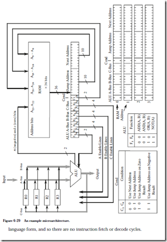
6.17 A microarchitecture is shown in Figure 6-29. The datapath has four registers and an ALU. The control section is a finite state machine, in which there is a RAM and a register. For this microarchitecture, a compiler translates a high level program directly into microcode; there is no intermediate assembly

image

For this problem, you are to write the microcode that implements the instructions listed below. The microcode should be stored in locations 0, 1, 2, and 3 of the RAM. Although there are no lines that show it, assume that the n and z bits are both 0 when C0C1 = 00. That is, A23 and A22 are both 0 when there is no possible jump. Note: Each bit of the A, B, and C fields corresponds directly to a register. Thus, the pattern 1000 selects register R3, not register 8, which does not exist. There are some complexities with respect to how branches are made in this microarchitecture, but you do not need to be concerned with how this is done in order to generate the microcode.

image

6.18 In line 2047 of the ARC microprogram shown in Figure 6-15, would the program behave differently if the “GOTO 0” portion of the instruction is deleted?

6.19 In horizontal microprogramming, the microwords are wide, whereas in vertical microprogramming the words are narrow. In general, horizontal microwords can be executed quickly, but require more space than vertical microwords, which take more time to execute. If we make the microword for- mat shown in Figure 6-11 more horizontal by expanding the A, B, and C fields to contain a single bit for each of the 38 registers instead of a coded six-bit version, then we can eliminate the A, B, and C decoders shown in Figure 6-3. This allows the clock frequency to be increased, but also increases the space for the microstore.

(a) How wide will the new horizontal microword be?

(b) By what percentage will the microstore increase in size?

6.20 Refer to Figure 6-7. Show the ALU LUT0 and ALU LUTx (x > 0) entries for the INC(A) operation.

6.21 On some architectures, there is special hardware that updates the PC, which takes into account the fact that the rightmost two bits are always 0. There is no special hardware presented in this chapter for updating the PC,

and the branch microcode in lines 2 – 20 of Figure 6-15 has an error in how the PC is updated on line 12 because branch displacements are given in terms of words. Identify the error, and explain how to fix it.


Data path and control: case study: the vhdl hardware description language (background, what is vhdl?, a vhdl specification of the majority function and 9-value logic system).

6.3 Case Study: The VHDL Hardware Description Language

In this section we present a brief overview of VHDL (VHSIC Hardware

Description Language, in which VHSIC is yet another acronym for Very High Speed Integrated Circuit). Hardware description languages (HDLs), like VHDL and AHPL, are languages used for describing computer hardware, focusing primarily on logic devices and IC design. In the case of VHDL, however, designs can be specified at many different levels. For example, the control unit implemented in this chapter could be specified in VHDL.

We first cover the background that led to the development of VHDL, and then describe some of its properties. We then take a look at a VHDL specification of the majority function.

6.3.1 BACKGROUND

VHDL was the result of a collaboration between the Department of Defense (DOD), and many US industries. DOD, primarily through its Defense Advanced Research Products Agency (DARPA), realized in the late 1970’s that IC design and fabrication was becoming so complex that a set of integrated design tools was needed for both design and simulation. It was felt that the tools should allow the user to specify a circuit or system from the highest, or behavioral level down to the lowest levels of actual IC layout and design, and further- more, all of these specifications should be verifiable by simulators and other rule checkers.

The first preliminary requirements definition for the language was issued by DOD in 1981, as a recognition of the need for a more consistent approach to computer hardware design. The contract for the first version of the language was won by a consortium of IBM, Texas Instruments, and Intermetrics, a software engineering firm specializing in programming language design and implementation.

The consortium released a preliminary version for testing and comment in 1985. An updated version was submitted to the IEEE for standardization in 1986, the result being named IEEE 1076-1987. In 1993, a newer version, IEEE 1076-1993, was approved that addressed a number of minor problems and added several new features.

By almost any measure VHDL is a success, with many users both inside and out- side the defense contractor community. DOD now requires that all Applica- tion-Specific Integrated Circuits (ASICs) be accompanied by their VHDL model for checking and simulation. Almost all CAD vendors now support VHDL in their toolsets.

6.3.2 WHAT IS VHDL?

In its most basic terms VHDL is a hardware description language that can be used to describe and model digital systems. VHDL has an inherent sense of time, and can manage the progression of events through time. Unlike most procedural languages that are in common use, VHDL supports concurrent execution, and is event driven.

Concurrent execution

Concurrent execution means that unless special efforts are taken to specify sequential execution, all of the statements in a VHDL specification are executed in parallel. This is the way it should be, since when power is applied to a digital system the system runs “in parallel.” That is, current flows through circuits according to the rules of physics and logic, without any inherent sense of “which came first.”

Event-driven systems

VHDL deals with signals propagating through digital systems, and therefore log- ically and naturally supports the concept of changes in state as a function of time. Having a sense of time, it supports concepts such as “after,” “until,” and “wait.” As an event-driven system, it begins execution by executing any initialization code, and then records all changes in signal values, from 0®1 and 1®0, occur- ring at the inputs and outputs of components. It records these changes, or events, in a time-ordered queue, known as the event queue. It examines these events and if an event has an effect upon some component, that effect is evaluated. If the effect causes further events to take place the simulator likewise places these new events in the event queue, and the process continues until and unless there are no further events to process.

Levels of abstraction, and hierarchical decomposition

As mentioned above, VHDL specifications can be written at almost any level of abstraction from the purely algorithmic level, where behavior is specified by for- mal algorithms, to the logic level, where behavior is specified by Boolean expressions.

Furthermore, a VHDL specification may be composed of a hierarchy of components, that is, components may contain components, which may themselves contain components. This models the physical world, where, for example, a motherboard may contain IC chips, which are composed of modules, which are in turn composed of sub-modules, all the way down to individual logic gates, and finally transistors.

6.3.3 A VHDL SPECIFICATION OF THE MAJORITY FUNCTION

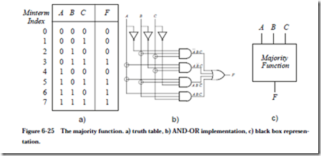
Let us explore how VHDL can be used to implement a small digital component by examining several implementations of the majority function, which produces a 1 at its output when more than half of its inputs are 1, otherwise it produces a 0 at its output. This is a useful function for fault tolerance, in which multiple systems that perform the same operations on the same data set “vote,” and if one of the systems deviates from the others, its output is effectively ignored. The majority function is discussed in detail in Appendix A. Its truth table is shown in Figure A-15 and Figure A-16, reproduced here as Figure 6-25.

image

In VHDL the specification of any component such as the majority function is split into two parts, an entity part and an architecture part. These correspond roughly to the syntactic and semantic parts of a language specification: the entity part describes the interface of the component without saying anything about its internal structure. The architecture part describes the internal behavior of the component. Here is an entity specification for the 3-input majority function:

Interface specification for the majority component

image

Keywords are shown in bold, and comments begin with “–” and end at the end of the line. Statements are separated by semicolons, “;”.

The entity specification describes just the “black box” input and output sig- nals in Figure 6-25c. The port declaration describes the kind of signals going into and out of the entity. Port modes include in for signals that flow into the entity, out for signals that flow out of the entity, and inout for bidirectional signals. There are also several other special purpose port modes.

With the interface to the majority component specified we can now model the internal functioning of the component, using the architecture specification:

Behavioral model for the majority component

image

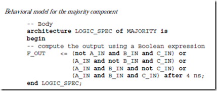
This model describes the relationship between the entity declaration of MAJOR- ITY and the architecture of MAJORITY. The names A_IN, B_IN, C_IN, and F_OUT in the architecture model must match the names used in the entity declaration.

This kind of architectural specification is referred to as a behavioral one, since it defines the input/output function by specifying an explicit transfer function. That function is a Boolean expression that implements the Boolean function shown in Figure 6-25a,b. Notice, however, that even at this level of specification

that we can include a time delay between inputs and outputs, using the after keyword. In this case, the event computing the value of F_OUT will be triggered 4 ns after a change in any of the input values.

It is also possible to specify the architecture at a level closer to the hardware by specifying logic gates instead of logic equations. This is referred to as a structural model. Here is such a specification:

Structural model for the majority component

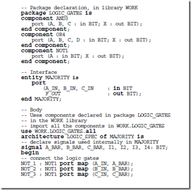
In generating a structural model for the MAJORITY entity we will follow the gate design given in Figure 6-25b. We begin the model by describing a collection of logic operators, in a special construct of VHDL known as a package. The package is assumed to be stored in a working library called WORK. Following the package specification we repeat the entity declaration, and then, using the package and entity declarations we specify the internal workings of the majority component by specifying the architecture at a structural level:

image

image

The package declaration supplies three gates, a 3-input AND gate, AND3, a 4-input OR gate, OR4, and a NOT gate, NOT1. The architectures of these gates are assumed to be declared elsewhere in the package. The entity declaration is unchanged, as we would expect, since it specifies MAJORITY as a “black box.”

The body specification begins with a use clause, which imports all of the declarations in the LOGIC_GATES package within the WORK library. The signal declaration declares seven BIT signals that will be used internally. These signals are used to interconnect the components within the architecture.

The instantiations of the three NOT gates follow, NOT_1, NOT_2, and NOT_3, all of which are NOT1 gates, and the mapping of their input and out- put signals are specified, following the port map keywords. Signals at the inputs and outputs of the logic gates are mapped according to the order in which they were declared within the package.

The rest of the body specification connects the NOT gates, the AND gates, and the OR gate together as shown in Figure 6-25b.

Notice that this form of architecture specification separates the design and implementation of the logic gates from the design of the MAJORITY entity. It would be possible to have several different implementations of the logic gates in different packages, and to use any one of them by merely changing the uses clause.

6.3.4 9-VALUE LOGIC SYSTEM

This brief treatment of VHDL only gives a small taste of the scope and power of the language. The full language contains capabilities to specify clock signals and various timing mechanisms, sequential processes, and several different kinds of signals. There is an IEEE standard 9-value logic system, known as STD_ULOGIC, IEEE 1164-1993. It has the following logic values:

image

Without getting into too much detail, these values allow the user to detect logic flaws within a design, and to follow the propagation of uninitialized or weak signals through the design.


Data path and control: hardwired control.

Hardwired Control

An alternative approach to a micro programmed control unit is to use a hard- wired approach, in which a direct implementation is created using flip-flops and logic gates, instead of using a control store and a microword selection mechanism. States in a finite state machine replace steps in the microprogram.

In order to manage the complexity of design for a hardwired approach, a hard- ware description language (HDL) is frequently used to represent the control structure. One example of an HDL is VHDL, which is an acronym for VHSIC Hardware Description Language (in which VHSIC is yet another acronym for Very High Speed Integrated Circuit). VHDL is used for describing an architecture at a very high level, and can be compiled into hardware designs through a process known as silicon compilation. For the hardwired control unit we will design here, a lower level HDL that is sometimes referred to as a register transfer language (RTL) is more appropriate.

We will define a simple HDL/RTL in this section that loosely resembles Hill & Peterson’s A Hardware Programming Language (AHPL) (Hill and Peterson, 1987). The general idea is to express a control sequence as a series of numbered statements, which can then be directly translated into a hardware design. Each statement consists of a data portion and a transfer portion, as shown below:

image

The statement is labelled “5,” which means that it is preceded by statement 4 and is succeeded by statement 6, unless an out-of-sequence transfer of control takes place. The left arrow (¬) indicates a data transfer, to register A for this case. The “ADD(B,C)” construct indicates that registers B and C are sent to a combinational logic unit (CLU) that performs the addition. Comments begin with an exclamation mark (!) and terminate at the end of the line. The GOTO construct indicates a transfer of control. For this case, control is transferred to statement 10 if bit 12 of register IR is true, otherwise control is transferred to the next higher numbered statement (6 for this case).

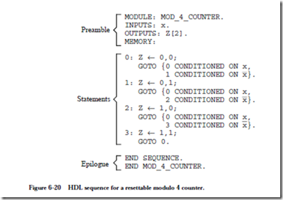
Figure 6-20 shows an HDL description of a modulo 4 counter. The counter produces the output sequence: 00, 01, 10, 11 and then repeats as long as the input line x is 0. If the input line is set to 1, then the counter returns to state 0 at the end of the next clock cycle. The comma is the catenation operator, and so the statement “Z ¬ 0,0;” assigns the two-bit pattern 00 to the two-bit output Z.

The HDL sequence is composed of three sections: the preamble, the numbered statements, and the epilogue. The preamble names the module with the “MODULE” keyword and declares the inputs with the “INPUTS” keyword, the outputs with the “OUTPUTS” keyword, and the arity (number of signals) of both, as well as any additional storage with the “MEMORY” keyword (none for this example). The numbered statements follow the preamble. The epilogue closes the sequence with the key phrase “END SEQUENCE.” The key phrase “END

image

MOD_4_COUNTER” closes the description of the module. Anything that appears between “END SEQUENCE” and “END MOD_4_COUNTER” occurs continuously, independent of the statement number. There are no such statements for this case.

In translating an HDL description into a design, the process can be decomposed into separate parts for the control section and the data section. The control section deals with how transitions are made from one statement to another. The data section deals with producing outputs and changing the values of any memory elements.

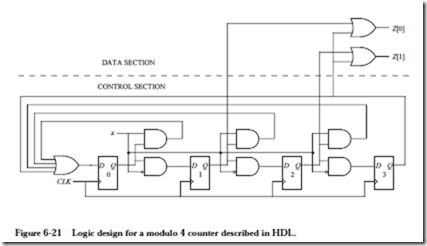
We consider the control section first. There are four numbered statements, and so we will use four flip-flops, one for each statement, as illustrated in Figure 6-21. This is referred to as a one-hot encoding approach, because exactly one flip-flop holds a true value at any time. Although four states can be encoded using only two flip-flops, studies have shown that the one-hot encoding approach results in approximately the same circuit area when compared with a more densely encoded approach; but more importantly, the complexity of the transfers from one state to the next are generally simpler and can be implemented with shallow combinational logic circuits, which means that the clock rate can be faster for a one-hot encoding approach than for a densely encoded approach.

In designing the control section, we first draw the flip-flops, apply labels as

image

appropriate, and connect the clock inputs. The next step is to simply scan the numbered statements in order and add logic as appropriate for the transitions. From statement 0, there are two possible transitions to statements 0 or 1, conditioned on x or its complement, respectively. The output of flip-flop 0 is thus connected to the inputs of flip-flops 0 and 1, through AND gates that take the value of the x input into account. Note that the AND gate into flip-flop 1 has a circle at one of its inputs, which is a simplified notation that means x is complemented by an inverter before entering the AND gate.

A similar arrangement of logic gates is applied for statements 1 and 2, and no logic is needed at the output of flip-flop 3 because statement 3 returns to statement 1 unconditionally. The control section is now complete and can execute correctly on its own. No outputs are produced, however, until the data section is implemented.

We now consider the design of the data section, which is trivial for this case. Both bits of the output Z change in every statement, and so there is no need to condition the generation of an output on the state. We only need to produce the correct output values for each of the statements. The least significant bit of Z is true in statements 1 and 3, and so the outputs of the corresponding control flip-flops are ORed to produce Z[0]. the most significant bit of Z is true in statements 2 and 3, and so the outputs of the corresponding control flip-flops are ORed to produce Z[1]. The entire circuit for the mod 4 counter is now complete, as shown in Figure 6-21.

We can now use our HDL in describing the control section of the ARC microarchitecture. There is no need to design the data section, since we have already defined its form in Figure 6-10. The data section is the same for both the micro- coded and hardwired approaches. As for the microcoded approach, the opera- tions that take place for a hardwired approach are:

1) Fetch the next instruction to be executed from memory.

2) Decode the opcode.

3) Read operand(s) from main memory or registers, if any.

4) Execute the instruction and store results.

5) Go to Step 1.

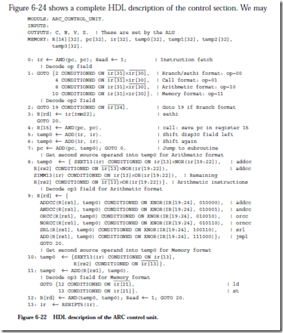
The microcode of Figure 6-15 can serve as a guide for what needs to be done. The first step is to fetch the next user-level instruction from main memory. The following HDL line describes this operation:

image

The structure of this statement is very similar to the first line of the microprogram, which may not be surprising since the same operations must be carried out on the same datapath.

Now that the instruction has been fetched, the next operation is to decode the opcode. This is where the power of a hardwired approach comes into play. Since every instruction has an op field, we can decode that field first, and then decode the op2, op3, and cond fields as appropriate for the instruction.

The next line of the control sequence decodes the op field:

image

The product symbol “X” indicates a logical AND operation. Control is thus transferred to one of the four numbered statements: 2, 4, 8, or 10 depending on the bit pattern in the op field.

image

have to do additional decoding depending on the value of the op field. At line 4, which is for the Call format, no additional decoding is necessary. The call instruction is then implemented in statements 4-7, which are similar to the microcoded version.

image

In statement 2, additional decoding is performed on the op2 field which is checked to determine if the instruction is sethi or a branch. Since there are only two possibilities, only one bit of op2 needs to be checked in line 2. Line 3 then implements sethi and line 19 implements the branch instructions.

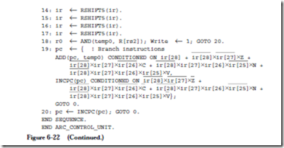
Line 8 begins the Arithmetic format section of the code. Line 8 gets the second source operand, which can be either immediate or direct, and can be sign extended to 32 bits (for addcc) or not sign extended. Line 9 implements the Arithmetic format instructions, conditioned on the op3 field. The XNOR function returns true if its arguments are equal, otherwise it returns false, which is useful in making comparisons.

Line 10 begins the Memory format section of the code. Line 10 gets the second source operand, which can either be a register or an immediate operand. Line 11 decodes the op3 field. Since the only Memory format instructions are ld and st, only a single bit (IR[21]) needs to be observed in the op3 field. Line 12 then implements the ld instruction, and lines 13-18 implement the st instruction. Finally, line 20 increments the program counter and transfers control back to the first statement.

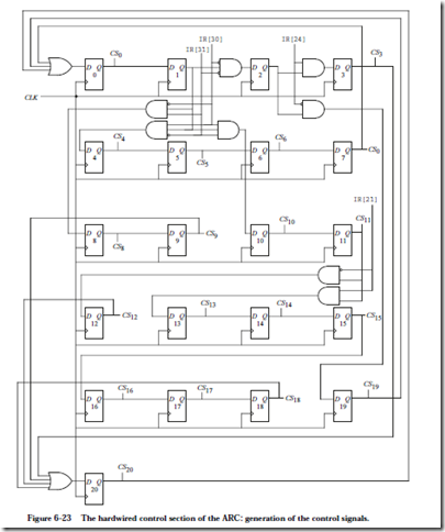
Now that the control sequence is defined, the next step is to design the logic for the control section. Since there are 21 statements, there are 21 flip-flops in the control section as shown in Figure 6-23. A control signal (CSi) is produced for each of the 21 states, which is used in the data section of the hardwired controller.

image

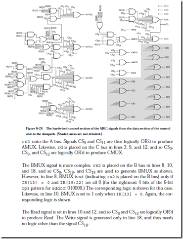
In Figure 6-24, the data section of the hardwired controller generates the signals that control the datapath. There are 27 OR gates that correspond to the 27 signals that control the datapath. (Refer to Figure 6-10. Count the 27 signals that originate in the control section that terminate in the datapath.) The AMUX signal is set to 1 only in lines 9 and 11, which correspond to operations that place

image

There are 4 signals that control the ALU: ALU[0], ALU[1], ALU[2], and ALU[3], which correspond to F0, F1, F2, and F3, respectively, in the ALU operation table shown in Figure 9-4. These four signals need values in each of the 20 HDL lines. In line 0, the ALU operation is AND, which corresponds to ALU[3:0] = 0101. Line 1 has no ALU operation specified, and so we can arbitrarily choose an ALU operation that has no side effects, like AND (0101). Continuing in this way, taking CONDITIONED ON statements into account, produces the logic for ALU[3:0] as shown in the figure.

The control signals are sent to the datapath, similar to the way that the MIR controls the datapath in the microprogrammed approach of Figure 6-10. The hard- wired and microcontrolled approaches can thus be considered interchangeable, except with varying costs. There are only 21 flip-flops in the hardwired approach, but there are 2048´41 = 83,968 flip-flops in the microprogrammed approach (although in actuality, a ROM would be used, which consumes less space because smaller storage elements than flip/flops can be used.) The amount of additional combinational logic is comparable. The hardwired approach is faster in executing ARC instructions, especially in decoding the Branch format instructions, but is more difficult to change once it is committed to fabrication.

EXAMPLE

Consider adding the same subcc instruction from the previous EXAMPLE to the hardwired implementation of the ARC instruction set. As before, the subcc instruction uses the Arithmetic format and an op3 field of 001100.

Only line 9 of the HDL code needs to be changed, by inserting the expression: ADDCC (R[rs1], INC_1(temp0)) CONDITIONED ON XNOR(IR[19:24], 001100), ! subcc before the line for addcc. The corresponding signals that need to be modified are ALU[3:0]. The INC_1 construct in the line above indicates that an adder CLU, which would be defined in another HDL module, should be created (in a hardwired control unit, there is a lot of flexibility on what can be done.)


Data path and control: a micro architecture for the arc (timing, developing the micro program, traps and interrupts and nanoprogramming).

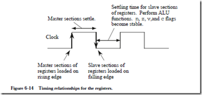
TIMING

The microarchitecture operates on a two-phase clock cycle, in which the master sections of all of the registers change on the rising edge of the clock and the slave sections change on the falling edge of the clock as shown in Figure 6-14. All of the registers use falling edge-triggered master/slave D flip-flops except for %r0
image

which does not need flip-flops. On the falling edge of the clock, data stored in the master sections of the registers are clocked into the slave sections. This makes the data available for operations involving the ALU. While the clock is low, the ALU, CBL, and MUX functions are performed, which settle in time for the rising edge of the clock. On the rising edge of the clock, the new values of the registers are written into the master sections. The registers settle while the clock is high, and the process then repeats.

DEVELOPING THE MICROPROGRAM

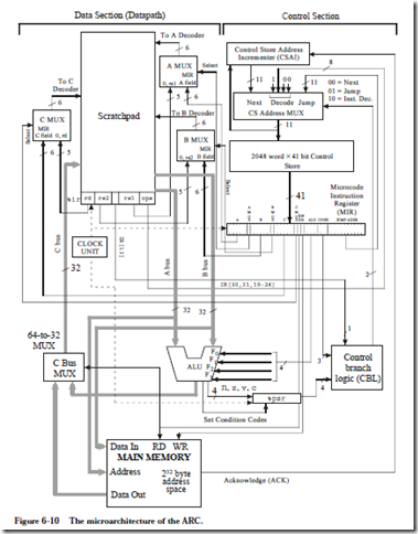
In a micro programmed architecture, instructions are interpreted by the micro- program in the control store. The micro program is often referred to as firmware because it bridges the gap between the hardware and the software. The microarchitecture shown in Figure 6-10 needs firmware in order to execute ARC instructions, and one possible coding is described in this section.

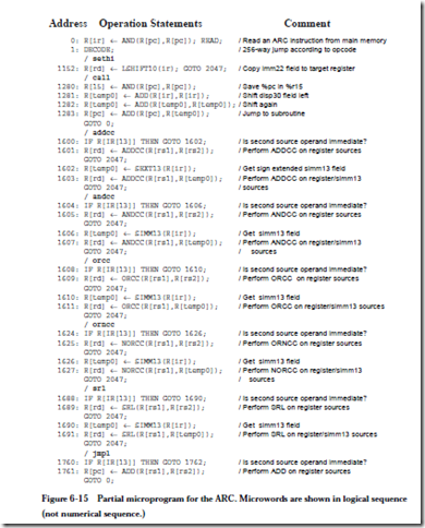
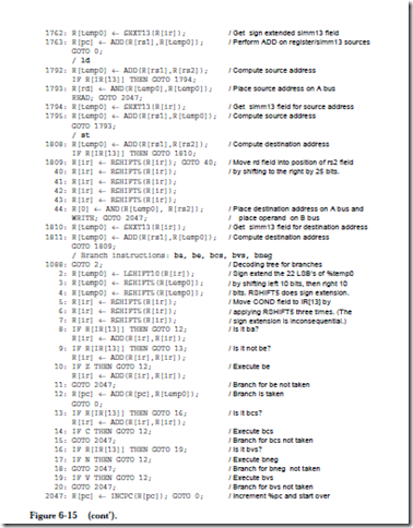
A portion of a microprogram that implements the fetch-execute cycle for the ARC is shown in Figure 6-15. In the control store, each microstatement is stored in coded form (1’s and 0’s) in a single microword. For simplicity, the micro-assembly language shown in Figure 6-15 is loosely defined here, and we will leave out labels, pseudo-ops, etc., that we would normally associate with a full-featured assembly language. Translation to the 41-bit format used in the microstore is not difficult to perform by hand for a small microprogram, and is frequently performed manually in practice (as we will do here) rather than creating a suite of software tools for such a small program.

Although our micro-assembly language is indeed an assembly language, it is not the same kind of assembly language as the ARC that we studied in Chapter 4.
image

The ARC assembly language is visible to the user, and is used for coding general purpose programs. Our micro-assembly language is used for coding firmware, and is not visible to the user. The sole purpose of the firmware is to interpret a user-visible instruction set. A change to the instruction set involves changes to the firmware, whereas a change in user-level software has no influence on the firmware.
image

Each statement in the microprogram shown in Figure 6-15 is preceded by a decimal number that indicates the address of the corresponding microword in the 2048-word control store. The address is followed by a colon. The operation statements follow the address, and are terminated by semicolons. An optional comment follows the operation field and begins with a slash ‘/.’ The comment terminates at the end of the line. More than one operation is allowed per line, as long as all of the operations can be performed in a single instruction cycle. The ALU operations come from Figure 6-4, and there are a few others as we will see. Note that the 65 statements are shown in logical sequence, rather than in numerical sequence.

Before the microprogram begins execution, the PC is set up with the starting address of a program that has been loaded into the main memory. This may hap- pen as the result of an initialization sequence when the computer is powered on, or by the operating system during the normal course of operation.

The first task in the execution of a user-level program is to bring the instruction pointed to by the PC from the main memory into the IR. Recall from Figure 6-10 that the address lines to main memory are taken from the A bus. In line 0, the PC is loaded onto the A bus, and a Read operation is initiated to memory. The notation “R[x]” means “register x,” in which x is replaced with one of the registers in the datapath, and so “R[1]” means “register %r1,” “R[ir]” means “register %ir,” and “R[rs1]” means the register that appears in the 5-bit rs1 field of an instruction (refer to Figure 6-2.)

The expression “AND(R[pc],R[pc])” simply performs a logical AND of %pc with itself in a literal interpretation. This operation is not very useful in a logical sense, but what we are interested in are the side effects. In order to place %pc onto the A bus, we have to choose an ALU operation that uses the A bus but does not affect the condition codes. There is a host of alternative choices that can be used, and the AND approach is arbitrarily chosen here. Note that the result of the AND operation is discarded because the C bus MUX in Figure 6-10 only allows the data output from main memory onto the C bus during a read operation.

A read operation normally takes more time to complete than the time required for one microinstruction to execute. The access time of main memory can vary depending on the memory organization, as we will see in Chapter 7. In order to account for variations in the access times of memory, the control store address incrementer (CSAI) does not increment the address until an acknowledge (ACK) signal is sent which indicates the memory has completed its operation.

Flow of control within the microprogram defaults to the next higher numbered statement unless a GOTO operation or a DECODE operation is encountered, and so microword 1 (line 1) is read into the MIR on the next cycle. Notice that some of the microcode statements in Figure 6-15 take up more than one line on the page, but are part of a single microinstruction. See, for example, lines 1283 and 1601.

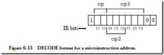
Now that the instruction is in the IR as a result of the read operation in line 0, the next step is to decode the opcode fields. This is performed by taking a 256-way branch into the microcode as indicated by the DECODE keyword in line 1 of the microprogram. The 11-bit pattern for the branch is constructed by appending a 1 to the left of bits 30 and 31 of the IR, followed by bits 19-24 of the IR, followed by the pattern 00. After the opcode fields are decoded, execution of the microcode continues according to which of the 15 ARC instructions is being interpreted.

As an example of how the decode operation works, consider the addcc instruction. According to the Arithmetic instruction format in Figure 6-2, the op field is 10 and the op3 field is 010000. If we append a 1 to the left of the op bit pat- tern, followed by the op3 bit pattern, followed by 00, the DECODE address is 11001000000 = (1600)10. This means that the microinstructions that interpret the addcc instruction begin at control store location 1600.

A number of DECODE addresses should never arise in practice. There is no Arithmetic instruction that corresponds to the invalid op3 field 111111, but if this situation does arise, possibly due to an errant program, then a microstore routine should be placed at the corresponding DECODE address 11011111100 = (1788)10 in order to deal with the illegal instruction. These locations are left blank in the microprogram shown in Figure 6-15.

Instructions in the SETHI/Branch and Call formats do not have op3 fields. The SETHI/Branch formats have op and op2 fields, and the Call format has only the op field. In order to maintain a simple decoding mechanism, we can create duplicate entries in the control store. Consider the SETHI format. If we follow the rule for constructing the DECODE address, then the DECODE address will have a 1 in the leftmost position, followed by 00 for the op field, followed by 100 which identifies SETHI in bit positions 19 – 21, followed by the bits in positions 22 – 24 of the IR, followed by 00, resulting in the bit pattern 100100xxx00 where xxx can take on any value, depending on the imm22 field. There are eight possible bit patterns for the xxx bits, and so we need to have duplicate SETHI codes at locations 10010000000, 10010000100, 10010001000, 10010001100, 10010010000, 10010010100, 10010011000, and 10010011100. DECODE addresses for the Branch and CALL formats are constructed in duplicate locations in a similar manner. Only the lowest addressed version of each set of duplicate codes is shown in Figure 6-15.

Although this method of decoding is fast and simple, a large amount of control store memory is wasted. An alternative approach that wastes much less space is to modify the decoder for the control store so that all possible branch patterns for SETHI point to the same location, and the same for the Branch and Call format instructions. For our microarchitecture, we will stay with the simpler approach and pay the price of having a large control store.

Consider now how the ld instruction is interpreted. The microprogram begins at location 0, and at this point does not know that ld is the instruction that the PC points to in main memory. Line 0 of the microprogram begins the Read operation as indicated by the READ keyword, which brings an instruction into the IR from the main memory address pointed to by the PC. For this case, let us assume that the IR now contains the 32-bit pattern:

image

which is a translation of the ARC assembly code: ld %r5 + 80, %r2. Line 1 then performs a branch to control store address (11100000000)2 = (1792)10.

At line 1792, execution of the ld instruction begins. In line 1792, the immediate bit i is tested. For this example, i = 1, and so control is transferred to microword 1794. If instead we had i = 0, then control would pass to the next higher numbered microword, which is 1793 for this case. Line 1792 adds the registers in the rs1 and rs2 fields of the instruction, in anticipation of a non-immediate form of ld, but this only makes sense if i = 0, which it is not for this example. The result that is stored in %temp0 is thus discarded when control is transferred to microword 1794, but this introduces no time penalty and does not produce any unwanted side effects (ADD does not change the condition codes).

In microword 1794, the simm13 field is extracted (using sign extension, as indicated by the SEXT13 operation), which is added with the register in the rs1 field in microword 1795. Control is then passed to microword 1793 which is where the READ operation takes place. Control passes to line 2047 where the PC is incremented in anticipation of reading the next instruction from main memory. Since instructions are four bytes long and must be aligned on word bound- aries in memory, the PC is incremented by four. Control then returns to line 0 where the process repeats. A total of seven microinstructions are thus executed in

interpreting the ld instruction. These microinstructions are repeated below:

image

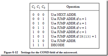
The remaining instructions, except for branches, are interpreted similar to the way ld is interpreted. Additional decoding is needed for the branch instructions because the type of branch is determined by the COND field of the branch format (bits 25 – 28), which is not used during a DECODE operation. The approach used here is to shift the COND bits into IR[13] one bit at a time, and then jump to different locations in the microcode depending on the COND bit pattern.

For branch instructions, the DECODE operation on line 2 of the microprogram transfers control to location 1088. We need more space for the branch instructions than the four-word per instruction allocation, so line 1088 transfers control to line 2 which is the starting address of a large section of available control store memory.

Lines 2 – 4 extract the 22-bit displacement for the branch by zeroing the high order 10 bits and storing the result in %temp0. This is accomplished by shifting %ir to the left by 10 bits and storing it in %temp0, and then shifting the result back to the right by 10 bits. (Notice that sign extension is performed on the dis- placement, which may be negative. RSHIFT5 implements sign extension.) Lines 5 – 7 shift %ir to the right by 15 bits so that the most significant COND bit (IR[28]) lines up in position IR[13], which allows the Jump on IR[13]=1 operation to test each bit. Alternatively, we could shift the COND field to IR[31] one bit at a time, and use the Jump on n condition to test each bit. (Note that there is a subtle error in how the PC is updated in line 12. See Problem 6.21 for an explanation.)

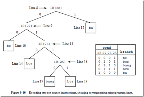
Line 8 starts the branch decoding process, which is summarized in Figure 6-16. If IR[28], which is now in IR[13], is set to 1, then the instruction is ba, which is executed in line 12. Notice that control returns to line 0, rather than to line 2047, so that the PC does not get changed twice for the same instruction.
image

If IR[28] is zero, then %ir is shifted to the left by one bit by adding it to itself, so that IR[27] lines up in position IR[13]. Bit IR[27] is tested in line 9. If IR[27] is zero, then the be instruction is executed in line 10, otherwise %ir is shifted to the left and IR[26] is then tested in line 13. The remaining branch instructions are interpreted in a similar manner.

Microassembly Language Translation

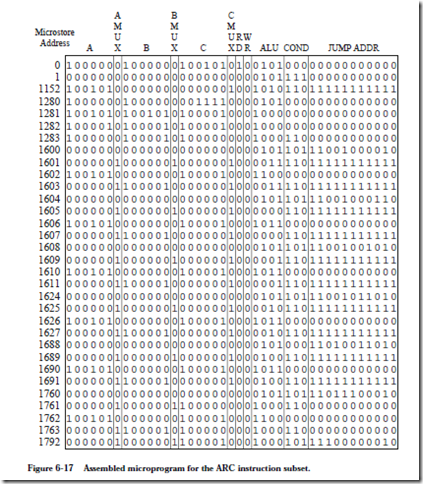
A microassembly language microprogram must be translated into binary object code before it is stored in the control store, just as an assembly language program must be translated into a binary object form before it is stored in main memory. Each line in the ARC microprogram corresponds to exactly one word in the control store, and there are no unnumbered forward references in the microprogram, so we can assemble the ARC microprogram one line at a time in a single pass. Consider assembling line 0 of the microprogram shown in Figure 6-15:

image

We can fill in the fields of the 41-bit microword as shown below:

image

The PC is enabled onto both the A and B busses for the AND operation, which transfers a word through the ALU without changing it. The A and B fields have the bit pattern for the PC (3210 = 1000002). The AMUX and BMUX fields both contain 0’s, since the inputs to these MUXes are taken from the MIR. The target of the Read operation is the IR, which has a corresponding bit pattern of (3710 = 1001012) for the C field. The CMUX field contains a 0 because the input to the CMUX is taken from the MIR. A read operation to memory takes place, and so the RD field contains a 1 and the WR field contains a 0. The ALU field contains 0101, which corresponds to the AND operation. Note that the condition codes are not affected, which would happen if ANDCC is used instead. The COND field contains 000 since control passes to the next microword, and so the bit pat- tern in the JUMP ADDR field does not matter. Zeros are arbitrarily placed in the JUMP ADDR field.

The second microword implements the 256-way branch. For this case, all that matters is that the bit pattern 111 appears in the COND field for the DECODE operation, and that no registers, memory, or condition codes are disturbed. The corresponding bit pattern is then:

image

A number of different bit patterns would also work for line 1. For example, any bit patterns can appear in the A, B, or JUMP ADDR fields when a DECODE operation takes place. The use of the zero bit patterns is an arbitrary choice. The ALU field is 0101 which is for AND, which does not affect the condition codes. Any other ALU operation that does not affect the condition codes can also be used.

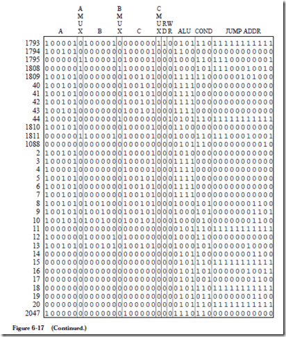
The remainder of the microprogram is translated in a similar manner. The trans-
image

lated microprogram is shown in Figure 6-17, except for gaps where duplicate branch code would appear, or where “illegal instruction” code would appear.

EXAMPLE

Consider adding an instruction called subcc to the microcoded implementation of the ARC instruction set, which subtracts its second source operand from the first, using two’s complement arithmetic. The new instruction uses the Arithmetic format and an op3 field of 001100.
image

We need to modify the microprogram to add this new instruction. We start by computing the starting location of subcc in the control store, by appending a ‘1’ to the left of the op field, which is 10, followed by the op3 field which is 001100, followed by 00. This results in the bit pattern 11000110000 which corresponds to control store location (1584)10. We can then create microassembly code that is similar to the addcc microassembly code at location 1600, except that the two’s complement negative of the subtrahend (the second source operand) is formed before performing the addition. The subtrahend is complemented by making use of the NOR operation, and 1 is added to it by using the INC operation. The subtraction is then completed by using the code for addcc. A  microassembly coding for subcc is shown below:

image

image


TRAPS AND INTERRUPTS

A trap is an automatic procedure call initiated by the hardware after an exceptional condition caused by an executing program, such as an illegal instruction, overflow, underflow, dividing by zero, etc. When a trap occurs, control is transferred to a “trap handler” which is a routine that is part of the operating system. The handler might do something like print a message and terminate the offending program.

One way to handle traps is to modify the microcode, possibly to check the status bits. For instance, we can check the v bit to see if an overflow has occurred. The microcode can then load an address into the PC (if a trap occurs) for the starting location of the trap handler.

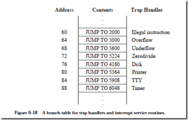
Normally, there is a fixed section of memory for trap handler starting addresses where only a single word is allocated for each handler. This section of memory forms a branch table that transfers control to the handlers, as illustrated in Figure 6-18. The reason for using a branch table is that the absolute addresses for each type of trap can be embedded in the microcode this way, while the targets of the jumps can be changed at the user level to handle traps differently.
image

A historically common trap is for floating point instructions, which may be emulated by the operating system if they are not implemented directly in hard- ware. Floating point instructions have their own opcodes, but if they are not implemented by the hardware (that is, the microcode does not know about them) then they will generate an illegal instruction trap when an attempt is made to execute them. When an illegal instruction occurs, control is passed to the illegal instruction handler which checks to see if the trap is caused by a floating point instruction, and then passes control to a floating point emulation routine as appropriate for the cause of the trap. Although floating point units are normally integrated into CPU chips these days, this method is still used when extending the instruction set for other instructions, such as graphics extensions to the ISA.

Interrupts are similar to traps, but are initiated after a hardware exception such as a user hitting a key on a keyboard, an incoming telephone call for a modem, a power fluctuation, an unsafe operating temperature, etc. Traps are synchronous with a running program, whereas interrupts are asynchronous. Thus, a trap will always happen at the same place in the same program running with the same data set, whereas the timing of interrupts is largely unpredictable.

When a key is pressed on an interrupt based keyboard, the keyboard asserts an interrupt line on the bus, and the CPU then asserts an acknowledge line as soon as it is ready (this is where bus arbitration comes in, which is covered in Chapter 8, if more than one device wants to interrupt at the same time). The keyboard then places an interrupt vector onto the data bus which identifies itself to the

CPU. The CPU then pushes the program counter and processor status register (where the flags are stored) onto the stack. The interrupt vector is used to index into the branch table, which lists the starting addresses of the interrupt service routines.

When a trap handler or an interrupt service routine begins execution, it saves the registers that it plans to modify on the stack, performs its task, restores the registers, and then returns from the interrupt. The process of returning from a trap is different from returning from a subroutine, since the process of entering a trap is different from a subroutine call (because the %psr register is also saved and restored). For the ARC, the rett instruction (see Chapter 8) is used for returning from a trap or interrupt. Interrupts can interrupt other interrupts, and so the first thing that an interrupt service routine might do is to raise its priority (using a special supervisor mode instruction) so that no interrupts of lower priority are accepted.

NANOPROGRAMMING

If the microstore is wide, and has lots of the same words, then we can save microstore memory by placing one copy of each unique microword in a nanostore, and then use the microstore to index into the nanostore. For instance, in the microprogram shown in Figure 6-15, lines 1281 and 1282 are the same. Lines 3, 4, and 40-44 are the same, and there are a number of other microin- structions that recur, especially for the duplicated branch microcode and the duplicated illegal instruction microcode.

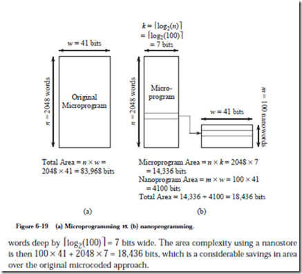
Figure 6-19a illustrates the space requirement for the original microstore ROM. There are n=2048 words that are each 41 bits wide, giving an area complexity of 2048 ´ 41 = 83,968 bits. Suppose now that there are 100 unique microwords in the ROM (the microprogram in Figure 6-15 is only partially complete so we can- not measure the number of unique microwords directly). Figure 6-19b illustrates a configuration that uses a nanostore, in which an area savings can be realized if there are a number of bit patterns that recur in the original microcode sequence. The unique microwords (100 for this case) form a nanoprogram, which is stored in a ROM that is 100 words deep by 41 bits wide.

The microprogram now indexes into the nanostore. The microprogram has the same number of microwords regardless of whether or not a nanostore is used, but when a nanostore is used, pointers into the nanostore are stored in the microstore rather than the wider 41-bit words. For this case, the microstore is now 2048
image

For small m and large n, where m is the length of the nanoprogram, we can realize a large savings in memory. This frees up area that can be applied in some other way, possibly to improve performance. However, instead of accessing only the microstore, we must now access the microstore first, followed by an access to the nanostore. The machine will thus run more slowly, but will fit into a smaller area.
 

Data path and control: a micro architecture for the arc (the data path and the control section).

6.1 A Micro architecture for the ARC

In this section we consider a micro programmed approach for designing the ARC control unit. We begin by describing the data path and its associated control signals.

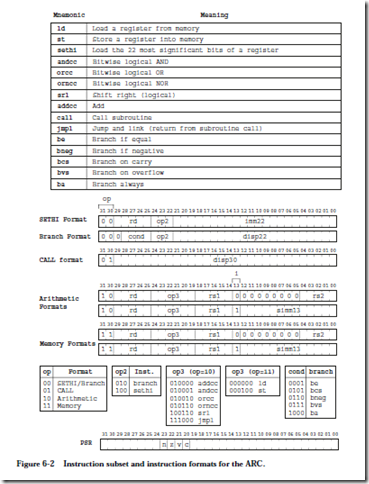
The instruction set and instruction format for the ARC subset is repeated from Chapter 4 in Figure 6-2. There are 15 instructions that are grouped into four for- mats according to the leftmost two bits of the coded instruction. The Processor Status Register % psr is also shown.

6.2.1 THE DATAPATH

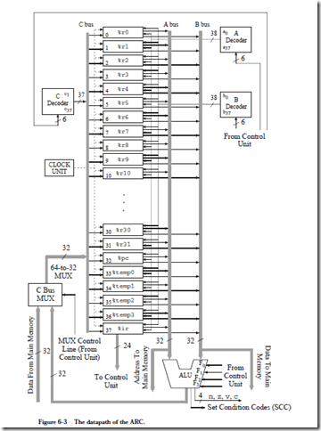
A datapath for the ARC is illustrated in Figure 6-3. The data path contains 32 user-visible data registers (%r0 – %r31), the program counter (%pc), the instruction register (%ir), the ALU, four temporary registers not visible at the ISA level (%temp0 – %temp3), and the connections among these components. The number adjacent to a diagonal slash on some of the lines is a simplification that indicates the number of separate wires that are represented by the corresponding single line.

Registers %r0 – %r31 are directly accessible by a user. Register %r0 always contains the value 0, and cannot be changed. The %pc register is the program counter, which keeps track of the next instruction to be read from the main memory. The user has direct access to %pc only through the call and jmpl instructions. The temporary registers are used in interpreting the ARC instruction set, and are not visible to the user. The %ir register holds the current instruction that is being executed. It is not visible to the user.

imageThe ALU

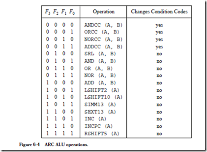
The ALU performs one of 16 operations on the A and B busses according to the table shown in Figure 6-4. For every ALU operation, the 32-bit result is placed on the C bus, unless it is blocked by the C bus MUX when a word of memory is placed onto the C bus instead.

image

The ANDCC and AND operations perform a bit-by-bit logical AND of corresponding bits on the A and B busses. Note that only operations that end with

image

“CC” affect the condition codes, and so ANDCC affects the condition codes whereas AND does not. (There are times when we wish to execute arithmetic and logic instructions without disturbing the condition codes.) The ORCC and OR operations perform a bit-by-bit logical OR of corresponding bits on the A and B busses. The NORCC and NOR operations perform a bit-by-bit logical NOR of corresponding bits on the A and B busses. The ADDCC and ADD operations carry out addition using two’s complement arithmetic on the A and B busses.

The SRL (shift right logical) operation shifts the contents of the A bus to the right by the amount specified on the B bus (from 0 to 31 bits). Zeros are copied into the leftmost bits of the shifted result, and the rightmost bits of the result are discarded. LSHIFT2 and LSHIFT10 shift the contents of the A bus to the left by two and 10 bits, respectively. Zeros are copied into the rightmost bits.

SIMM13 retrieves the least significant 13 bits of the A bus, and places zeros in the 19 most significant bits. SEXT13 performs a sign extension of the 13 least significant bits on the A bus to form a 32-bit word. That is, if the leftmost bit of the 13 bit group is 1, then 1’s are copied into the 19 most significant bits of the result, otherwise, 0’s are copied into the 19 most significant bits of the result. The INC operation increments the value on the A bus by 1, and the INCPC operation increments the value on the A bus by four, which is used in incrementing the PC register by one word (four bytes). INCPC can be used on any register placed on the A bus.

The RSHIFT5 operation shifts the operand on the A bus to the right by 5 bits, copying the leftmost bit (the sign bit) into the 5 new bits on the left. This has the effect of performing a 5-bit sign extension. When applied three times in succession to a 32-bit instruction, this operation also has the effect of placing the left- most bit of the COND field in the Branch format (refer to Figure 6-2) into the position of bit 13. This operation is useful in decoding the Branch instructions, as we will see later in the chapter. The sign extension for this case is inconsequential.

Every arithmetic and logic operation can be implemented with just these ALU operations. As an example, a subtraction operation can be implemented by forming the two’s complement negative of the subtrahend (making use of the NOR operation and adding 1 to it with INC) and then performing addition on the operands. A shift to the left by one bit can be performed by adding a number to itself. A “do-nothing” operation, which is frequently needed for simply passing data through the ALU without changing it, can be implemented by logically ANDing an operand with itself and discarding the result in %r0. A logical XOR can be implemented with the AND, OR, and NOR operations, making use of DeMorgan’s theorem (see problem 6.5).

The ALU generates the c, n, z, and v condition codes which are true for a carry, negative, zero, or overflow result, respectively. The condition codes are changed only for the operations indicated in Figure 6-4. A signal (SCC) is also generated that tells the %psr register when to update the condition codes.

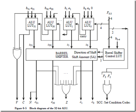
The ALU can be implemented in a number of ways. For the sake of simplicity, let us consider using a lookup table (LUT) approach. The ALU has two 32-bit data inputs A and B, a 32-bit data output C, a four-bit control input F, a four-bit condition code output (N, V, C, Z), and a signal (SCC) that sets the flags in the

%psr register. We can decompose the ALU into a cascade of 32 LUTs that implement the arithmetic and logic functions, followed by a barrel shifter that implements the shifts. A block diagram is shown in Figure 6-5.

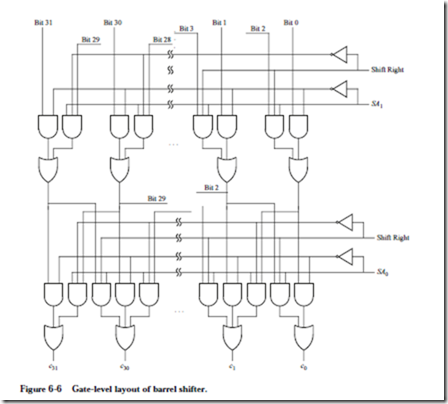
The barrel shifter shifts the input word by an arbitrary amount (from 0 to 31 bits) according to the settings of the control inputs. The barrel shifter performs shifts in levels, in which a different bit of the Shift Amount (SA) input is observed at each level. A partial gate-level layout for the barrel shifter is shown in

image

Figure 6-6. Starting at the bottom of the circuit, we can see that the outputs of the bottom stage will be the same as the inputs to that stage if the SA0 bit is 0. If the SA0 bit is 1, then each output position will take on the value of its immediate left or right neighbor, according to the direction of the shift, which is indicated by the Shift Right input. At the next higher level, the method is applied again, except that the SA1 bit is observed and the amount of the shift is doubled. The process continues until bit SA4 is observed at the highest level. Zeros are copied into positions that have no corresponding inputs. With this structure, an arbitrary shift from 0 to 31 bits to the left or the right can be implemented.

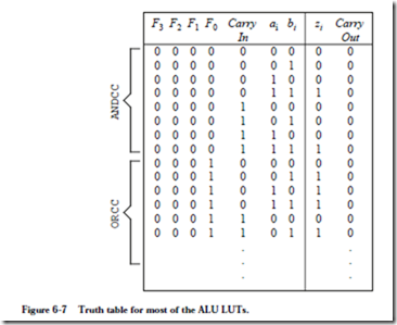
Each of the 32 ALU LUTs is implemented (almost) identically, using the same lookup table entries, except for changes in certain positions such as for the INC and INCPC operations (see problem Figure 6.20). The first few entries for each LUT are shown in Figure 6-7. The barrel shifter control LUT is constructed in a similar manner, but with different LUT entries.

image

The condition code bits n, z, v, and c are implemented directly. The n and c bits are taken directly from the c31 output of the barrel shifter and the carry-out position of ALU LUT31, respectively. The z bit is computed as the NOR over the barrel shifter outputs. The z bit is 1 only if all of the barrel shifter outputs are

0. The v (overflow) bit is set if the carry into the most significant position is different than the carry out of the most significant position, which is implemented with an XOR gate.

Only the operations that end in “CC” should set the condition codes, and so a signal is generated that informs the condition codes to change, as indicated by the label “SCC: Set Condition Codes.” This signal is true when both F3 and F2 are false.

The Registers

All of the registers are composed of falling edge-triggered D flip-flops (see Appen-

image

dix A). This means that the outputs of the flip-flops do not change until the clock makes a transition from high to low (the falling edge of the clock). The registers all take a similar form, and so we will only look at the design of register

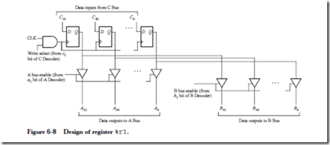
%r1. All of the datapath registers are 32 bits wide, and so 32 flip-flops are used for the design of %r1, which is illustrated in Figure 6-8.

image

The CLK input to register %r1 is ANDed with the select line (c1) from the C Decoder. This ensures that %r1 only changes when the control section instructs it to change. The data inputs to %r1 are taken directly from the corresponding

lines of the C bus. The outputs are written to the corresponding lines of the A and B busses through tri-state buffers, which are “electrically disconnected” unless their enable inputs are set to 1. The outputs of the buffers are enabled onto the A and B busses by the a1 and b1 outputs of the A and B decoders, respectively. If neither a1 nor b1 are high (meaning they are equal to 1), then the outputs of %r1 are electrically disconnected from both the A and B busses since the tri-state buffers are disabled.

The remaining registers take a similar form, with a few exceptions. Register %r0 always contains a 0, which cannot be changed. Register %r0 thus has no inputs from the C bus nor any inputs from the C decoder, and does not need flip-flops (see Problem 6.11). The %ir register has additional outputs that correspond to the rd, rs1, rs2, op, op2, op3, and bit 13 fields of an instruction, as illustrated in Figure 6-9. These outputs are used by the control section in interpreting

image

an instruction as we will see in Section 6.2.4. The program counter can only contain values that are evenly divisible by 4, and so the rightmost two bits in %pc can be hardwired to 0.

The A, B, and C decoders shown in Figure 6-3 simplify register selection. The six-bit inputs to the decoders select a single register for each of the A, B, and C busses. There are 26 = 64 possible outputs from the decoders, but there are only 38 data registers. The index shown to the left of each register (in base 10) in Figure 6-3 indicates the value that must be applied to a decoder input to select the corresponding register. The 0 output of the C decoder is not used because %r0 cannot be written. Indices that are greater than 37 do not correspond to any registers, and are free to be used when no registers are to be connected to a bus.

6.2.2 THE CONTROL SECTION

The entire microprogrammed ARC microarchitecture is shown in Figure 6-10.

image

The figure shows the datapath, the control unit, and the connections between them. At the heart of the control unit is a 2048 word ´ 41 bit read-only memory (ROM) that contains values for all of the lines that must be controlled to implement each user-level instruction. The ROM is referred to as a control store in this context. Each 41-bit word is called a microinstruction. The control unit is responsible for fetching microinstructions and executing them, much in the same way as user-level ARC macroinstructions are fetched and executed. This microinstruction execution is controlled by the microprogram instruction register (MIR), the processor status register (%psr), and a mechanism for determining the next microinstruction to be executed: the Control Branch Logic (CBL) unit and the Control Store (CS) Address MUX. A separate PC for the microprogram is not needed to store the address of the next microinstruction, because it is recomputed on every clock cycle and therefore does not need to be stored for future cycles.

When the microarchitecture begins operation (at power-on time, for example), a reset circuit (not shown) places the microword at location 0 in the control store into the MIR and executes it. From that point onward, a microword is selected for execution from either the Next, the Decode, or the Jump inputs to the CS Address MUX, according to the settings in the COND field of the MIR and the output of the CBL logic. After each microword is placed in the MIR, the datapath performs operations according to the settings in the individual fields of the MIR. This process is detailed below.

A microword contains 41 bits that comprise 11 fields as shown in Figure 6-11.

image

Starting from the left, the A field determines which of the registers in the datapath are to be placed on the A bus. The bit patterns for the registers correspond to the binary representations of the base 10 register indices shown in Figure 6-3 (000000 – 100101). The AMUX field selects whether the A Decoder takes its input from the A field of the MIR (AMUX = 0) or from the rs1 field of %ir (AMUX = 1).

In a similar manner, the B field determines which of the registers in the datapath are to be placed on the B bus. The BMUX field selects whether the B Decoder takes its input from the B field of the MIR (BMUX = 0) or from the rs2 field of %ir (BMUX = 1). The C field determines which of the registers in the datapath is to be written from the C bus. The CMUX field selects whether the C Decoder takes its input from the C field of the MIR (CMUX = 0) or from the rd field of %ir (CMUX = 1). Since %r0 cannot be changed, the bit pattern 000000 can be used in the C field when none of these registers are to be changed.

The RD and WR lines determine whether the memory will be read or written, respectively. A read takes place if RD = 1, and a write takes place if WR = 1. Both the RD and WR fields cannot be set to 1 at the same time, but both fields can be 0 if neither a read nor a write operation is to take place. For both RD and WR, the address for the memory is taken directly from the A bus. The data input to the memory is taken from the B bus, and the data output from the memory is placed on the C bus. The RD line controls the 64-to-32 C Bus MUX, which determines whether the C bus is loaded from the memory (RD = 1) or from the ALU (RD = 0).

The ALU field determines which of the ALU operations is performed according to the settings shown in Figure 6-4. All 16 possible ALU field bit patterns correspond to valid ALU operations. This means that there is no way to “turn the ALU off ” when it is not needed, such as during a read or write to memory. For this situation, an ALU operation should be selected that has no unwanted side effects. For example, ANDCC changes the condition codes and would not be appropriate, whereas the AND operation does not affect the condition codes, and would therefore be appropriate.

The COND (conditional jump) field instructs the microcontroller to take the next microword from either the next control store location, or from the location in the JUMP ADDR field of the MIR, or from the opcode bits of the instruction in %ir. The COND field is interpreted according to the table shown in Figure 6-12. If the COND field is 000, then no jump is taken, and the Next input to the CS Address MUX is used. The Next input to the CS Address MUX is computed by the control store address incrementer (CSAI) shown in Figure 6-10, which increments the current output of the CS Address MUX by 1. If the COND field is 001, 010, 011, 100, or 101, then a conditional jump is taken to the control store location in the JUMP ADDR field, according to the value of the n, z, v, or c flags, or bit 13 of %ir, respectively. The syntax “IR[13]” means “bit 13 of the instruction register %ir.” If the COND field is 110, then an unconditional jump is taken.

image

The bit pattern 111 is used in the COND field when an instruction is being decoded. When the COND field is 111, then the next control store location that is copied into the MIR is taken from neither the Next input to the CS Address MUX nor the Jump input, but is taken from a combination of 11 bits created by appending 1 to the left of bits 30 and 31 of %ir and appending 00 to the right of bits 19-24 of %ir. This DECODE address format is shown in Figure 6-13. The

image

purpose of using this addressing scheme is to allow an instruction to be decoded in a single step, by branching to a different location according to the settings in the op, op2, and op3 fields of an instruction.

Finally, the JUMP ADDR field appears in the rightmost 11 bits of the micro- word format. There are 211 microwords in the control store, and so 11 bits are needed in the JUMP ADDR field in order to jump to any microstore location.


Datapath and control : basic s of the microarchitecture

DATAPATH AND CONTROL

In the earlier chapters, we examined the computer at the Application Level, the High Level Language level, and the Assembly Language level (as shown in Figure 1-4.) In Chapter 4 we introduced the concept of an ISA: an instruction set that effects operations on registers and memory. In this chapter, we explore the part of the machine that is responsible for implementing these operations: the control unit of the CPU. In this context, we view the machine at the microarchitecture level (the Microprogrammed/Hardwired Control level in Figure 1-4.) The microarchitecture consists of the control unit and the programmer-visible registers, functional units such as the ALU, and any additional registers that may be required by the control unit.

A given ISA may be implemented with different microarchitectures. For example, the Intel Pentium ISA has been implemented in different ways, all of which support the same ISA. Not only Intel, but a number of competitors such as AMD and Cyrix have implemented Pentium ISAs. A certain microarchitecture might stress high instruction execution speed, while another stresses low power consumption, and another, low processor cost. Being able to modify the microarchitecture while keeping the ISA unchanged means that processor vendors can take advantage of new IC and memory technology while affording the user upward compatibility for their software investment. Programs run unchanged on different processors as long as the processors implement the same ISA, regardless of the underlying microarchitectures.

In this chapter we examine two polarizingly different microarchitecture approaches: microprogrammed control units and hardwired control units, and we examine them by showing how a subset of the ARC processor can be implemented using these two design techniques.

6.1 Basic s of the Microarchitecture

The functionality of the microarchitecture centers around the fetch-execute cycle, which is in some sense the “heart” of the machine. As discussed in Chapter 4, the steps involved in the fetch-execute cycle are:

1) Fetch the next instruction to be executed from memory.

2) Decode the opcode.

3) Read operand(s) from main memory or registers, if any.

4) Execute the instruction and store results.

5) Go to Step 1.

It is the microarchitecture that is responsible for making these five steps happen. The microarchitecture fetches the next instruction to be executed, determines which instruction it is, fetches the operands, executes the instruction, stores the results, and then repeats.

The microarchitecture consists of a data section which contains registers and an ALU, and a control section, as illustrated in Figure 6-1. The data section is also

image

referred to as the datapath. Microprogrammed control uses a a special purpose microprogram, not visible to the user, to implement operations on the registers and on other parts of the machine. Often, the microprogram contains many pro- gram steps that collectively implement a single (macro)instruction. Hardwired control units adopt the view that the steps to be taken to implement an opera- tion comprise states in a finite state machine, and the design proceeds using conventional digital design methods (such as the methods covered in Appendix A.) In either case, the datapath remains largely unchanged, although there may be minor differences to support the differing forms of control. In designing the ARC control unit, the microprogrammed approach will be explored first, and then the hardwired approach, and for both cases the datapath will remain unchanged.


Summary of languages and the machine

■ SUMMARY

A high level programming language like C or Pascal allows the low-level architecture of a computer to be treated as an abstraction. An assembly language program, on the other hand, takes a form that is very dependent on the underlying architecture. The instruction set architecture (ISA) is made visible to the programmer, who is responsible for handling register usage and subroutine linkage. Some of the complexity of assembly language programming is managed through the use of macros, which differ from subroutines or functions, in that macros generate in-line code at assembly time, whereas subroutines are executed at run time.

A linker combines separately assembled modules into a single load module, which typically involves relocating code. A loader places the load module in memory and starts the execution of the program. The loader may also need to perform relocation if two or more load modules overlap in memory.

In practice the details of assembly, linking and loading is highly system-dependent and language-dependent. Some simple assemblers merely produce executable binary files, but more commonly an assembler will produce additional information so that modules can be linked together by a linker. Some systems provide linking loaders that combine the linking task with the loading task. Others separate linking from loading. Some loaders can only load a program at the address specified in the binary file, while more commonly, relocating loaders can relocate pro- grams to a load-time-specified address. The file formats that support these processes are also operating-system dependent.

Before compilers were developed, programs were written directly in assembly language. Nowadays, assembly language is not normally used directly since compilers for high-level languages are so prevalent and also produce efficient code, but assembly language is still important for understanding aspects of computer architecture, such as how to link programs that are compiled for different calling conventions, and for exploiting extensions to architectures such as MMX and AltiVec.

■ FURTHER READING

Compilers and compilation are treated by (Aho et al, 1985) and (Waite and Carter, 1993). There are a great many references on assembly language programming. (Donovan, 1972) is a classic reference on assemblers, linkers, and loaders. (Gill et al., 1987) covers the 68000. (Goodman and Miller, 1993) serves as a good instructional text, with examples taken from the MIPS architecture. The appendix in (Patterson and Hennessy, 1998) also covers the MIPS architecture. (SPARC, 1992) deals specifically with the definition of the SPARC, and SPARC assembly language.

Aho, A. V., Sethi, R., and Ullman, J. D., Compilers, Addison Wesley Longman, Reading, Massachusetts (1985).

Donovan, J. J., Systems Programming, McGraw-Hill, (1972).

Gill, A., E. Corwin, and A. Logar, Assembly Language Programming for the 68000, Prentice-Hall, Englewood Cliffs, New Jersey, (1987).

Goodman, J. and K. Miller, A Programmer’s View of Computer Architecture, Saun- ders College Publishing, (1993).

Patterson, D. A. and J. L. Hennessy, Computer Organization and Design: The Hardware / Software Interface, 2/e, Morgan Kaufmann Publishers, San Mateo, California, (1998).

SPARC International, Inc., The SPARC Architecture Manual: Version 8, Prentice Hall, Englewood Cliffs, New Jersey, (1992).

Waite, W. M., and Carter, L. R., An Introduction to Compiler Construction, Harper Collins College Publishers, New York, New York, (1993).

■ PROBLEMS

5.1 Create a symbol table for the ARC segment shown below using a form similar to Figure 5-7. Use “U” for any symbols that are undefined.

image

5.2 Translate the following ARC code into object code. Assume that x is at location (4096)10.

image

image

5.3 Create a symbol table for the program shown in Figure 5-8, using a form similar to Figure 5-7.

5.4 Translate subroutine add_64 shown in Figure 5-8, including variables A,

B, and C, into object code.

5.5 A disassembler is a software program that reads an object module and recreates the source assembly language module. Given the object code shown below, disassemble the code into ARC assembly language statements. Since there is not enough information in the object code to determine symbol names, choose symbols as you need them from the alphabet, consecutively, from ‘a’ to ‘z.’

image

5.6 Given two macros push and pop as defined below, unnecessary instruc- tions can be inserted into a program if a push immediately follows a pop. Expand the macro definitions shown below and identify the unnecessary instructions.

image

image

5.7 Write a macro called return that performs the function of the jmp 1 statement as it is used in Figure 5-5.

5.8 In Figure 4-16, the operand x for sethi is filled in by the assembler, but the statement will not work as intended if x ³ 222 because there are only 22 bits in the imm22 field of the sethi format. In order to place an arbitrary 32-bit address into %r5 at run time, we can use sethi for the upper 22 bits, and then use addcc for the lower 10 bits. For this we add two new pseudo-ops: .high22 and .low10, which construct the bit patterns for the high 22 bits and the low 10 bits of the address, respectively. The construct:

image

Rewrite the calling routine in Figure 4-16 using .high22 and .low10 so that it works correctly regardless of where x is placed in memory.

5.9 Assume that you have the subroutine add_64 shown in Figure 5-8 avail-

able to you. Write an ARC routine called add_128 that adds two 64-bit numbers, making use of add_64. The two 128-bit operands are stored in memory locations that begin at x and y, and the result is stored in the memory location that begins at z.

5.10 Write a macro called subcc that has a usage similar to addcc, that sub- tracts its second source operand from the first.

5.11 Does ordinary, nonrecursive macro expansion happen at assembly time or at execution time? Does recursive macro expansion happen at assembly time or at execution time?

5.12 An assembly language programmer proposes to increase the capability of the push macro defined in Figure 5-9 by providing a second argument, arg2. The second argument would replace the addcc %r14, -4, %r14 with addcc arg2, -4, arg2. Explain what the programmer is trying to accomplish, and what dangers lurk in this approach.


Languages and the machine: case study: extensions to the instruction set – the intel mm x™ and motorola altivec simd instructions (background, the base architectures, vector registers, vector arithmetic operations, vector compare operations and case study summary).

Case Study: Extensions to the Instruction Set – The Intel MM X™ and Motorola AltiVec SIM Dinstructions.

As integrated circuit technology provides ever increasing capacity within the processor, processor vendors search for new ways to use that capacity. One way that both Intel and Motorola capitalized on the additional capacity was to extend their ISAs with new registers and instructions that are specialized for processing streams or blocks of data. Intel provides the MMX extension to their Pentium processors and Motorola provides the AltiVec extension to their PowerPC processors. In this section we will discuss why the extensions are useful, and how the two companies implemented them.

BACKGROUND

The processing of graphics, audio, and communication streams requires that the same repetitive operations be performed on large blocks of data. For example a graphic image may be several megabytes in size, with repetitive operations required on the entire image for filtering, image enhancement, or other processing. So-called streaming audio (audio that is transmitted over a network in real time) may require continuous operation on the stream as it arrives. Likewise 3-D image generation, virtual reality environments, and even computer games require extraordinary amounts of processing power. In the past the solution adopted by many computer system manufacturers was to include special purpose processors explicitly for handling these kinds of operations.

Although Intel and Motorola took slightly different approaches, the results are quite similar. Both instruction sets are extended with SIMD (Single Instruction stream / Multiple Data stream) instructions and data types. The SIMD approach applies the same instruction to a vector of data items simultaneously. The term “vector” refers to a collection of data items, usually bytes or words.

Vector processors and processor extensions are by no means a new concept. The earliest CRAY and IBM 370 series computers had vector operations or extensions. In fact these machines had much more powerful vector processing capabilities than these first microprocessor-based offerings from Intel and Motorola. Nevertheless, the Intel and Motorola extensions provide a considerable speedup in the localized, recurring operations for which they were designed. These extensions are covered in more detail below, but Figure 5-11 gives an introduction to

image

the process. The figure shows the Intel PADDB (Packed Add Bytes) instruction, which performs 8-bit addition on the vector of eight bytes in register MM0 with the vector of eight bytes in register MM1, storing the results in register MM0.

THE BASE ARCHITECTURES

Before we cover the SIMD extensions to the two processors, we will take a look at the base architectures of the two machines. Surprisingly, the two processors could hardly be more different in their ISAs.

The Intel Pentium

Aside from special-purpose registers that are used in operating system-related matters, the Pentium ISA contains eight 32-bit integer registers, with each register having its own “personality.” For example, the Pentium ISA contains a single accumulator (EAX) which holds arithmetic operands and results. The processor also includes eight 80-bit floating-point registers, which, as we will see, also serve as vector registers for the MMX instructions. The Pentium instruction set would be characterized as CISC (Complicated Instruction Set Computer). We will dis- cuss CISC vs. RISC (Reduced Instruction Set Computer) in more detail in Chapter 10, but for now, suffice it to say that the Pentium instructions vary in size from a single byte to 9 bytes in length, and many Pentium instructions accomplish very complicated actions. The Pentium has many addressing modes, and most of its arithmetic instructions allow one operand or the result to be in either memory or a register. Much of the Intel ISA was shaped by the decision to make it binary-compatible with the earliest member of the family, the 8086/8088, introduced in 1978. (The 8086 ISA was itself shaped by Intel’s decision to make it assembly-language compatible with the venerable 8-bit 8080, introduced in 1973.)

The Motorola PowerPC

The PowerPC, in contrast, was developed by a consortium of IBM, Motorola and Apple, “from the ground up,” forsaking backward compatibility for the ability to incorporate the latest in RISC technology. The result was an ISA with fewer, simpler instructions, all instructions exactly one 32-bit word wide, 32 32-bit general purpose integer registers and 32 64-bit floating point registers. The ISA employs the “load/store” approach to memory access: memory operands have to be loaded into registers by load and store instructions before they can be used. All other instructions must access their operands and results in registers.

As we shall see below, the primary influence that the core ISAs described above have on the vector operations is in the way they access memory.

VECTOR REGISTERS

Both architectures provide an additional set of dedicated registers in which vector operands and results are stored. Figure 5-12 shows the vector register sets for the two processors. Intel, perhaps for reasons of space, “aliases” their floating point registers as MMX registers. This means that the Pentium’s 8 64-bit floating-point

image

registers also do double-duty as MMX registers. This approach has the disadvantage that the registers can be used for only one kind of operation at a time. The register set must be “flushed” with a special instruction, EMMS (Empty MMX State) after executing MMX instructions and before executing floating-point instructions.

Motorola, perhaps because their PowerPC processor occupies less silicon, implemented 32 128-bit vector registers as a new set, separate and distinct from their floating-point registers.

Vector operands

Both Intel and Motorola’s vector operations can operate on 8, 16, 32, 64, and, in Motorola’s case, 128-bit integers. Unlike Intel, which supports only integer vectors, Motorola also supports 32-bit floating point numbers and operations.

Both Intel and Motorola’s vector registers can be filled, or packed, with 8, 16, 32, 64, and in the Motorola case, 128-bit data values. For byte operands, this results in 8 or 16-way parallelism, as 8 or 16 bytes are operated on simultaneously. This is how the SIMD nature of the vector operation is expressed: the same operation is performed on all the objects in a given vector register.

Loading to and storing from the vector registers

Intel continues their CISC approach in the way they load operands into their vector registers. There are two instructions for loading and storing values to and from the vector registers, MOVD and MOVQ, which move 32-bit doublewords and 64-bit quadwords, respectively. (The Intel word is 16-bits in size.) The syntax is:

image

In addition, in the Intel vector arithmetic operations one of the operands can be in memory, as we will see below.

Motorola likewise remained true to their professed RISC philosophy in their load and store operations. The only way to access an operand in memory is through the vector load and store operations. There is no way to move an operand between any of the other internal registers and the vector registers. All operands must be loaded from memory and stored to memory. Typical load opcodes are:

image

where vD stands for one of the 32 vector registers. The memory address of the operand is computed from (rA|0 + rB), where rA and rB represent any two of the integer registers r0-r32, and the “|0” symbol means that the value zero may be substituted for rA. The byte, half word, word, or doubleword is fetched from that address. (PowerPC words are 32 bits in size.)

The term “indexed” in the list above refers to the location where the byte, half- word or word will be stored in the vector register. The least significant bits of the memory address specify the index into the vector register. For example, LSB’s 011 would specify that the byte should be loaded into the third byte of the register. Other bytes in the vector register are undefined.

The store operations work exactly like the load instructions above except that the value from one of the vector registers is stored in memory.

VECTOR ARITHMETIC OPERATIONS

The vector arithmetic operations form the heart of the SIMD process. We will see that there is a new form of arithmetic, saturation arithmetic, and several new and exotic operations.

Saturation arithmetic

Both vector processors provide the option of doing saturation arithmetic instead of the more familiar modulo wraparound kind discussed in Chapters 2 and 3. Saturation arithmetic works just like two’s complement arithmetic as long as the results do not overflow or underflow. When results do overflow or under- flow, in saturation arithmetic the result is held at the maximum or minimum allowable value, respectively, rather than being allowed to wrap around. For example two’s complement bytes are saturated at the high end at +127 and at the low end at -128. Unsigned bytes are saturated at 255 and 0. If an arithmetic result overflows or underflows these bounds the result is clipped, or “saturated” at the boundary.

The need for saturation arithmetic is encountered in the processing of color information. If color is represented by a byte in which 0 represents black and 255 represents white, then saturation allows the color to remain pure black or pure white after an operation rather than inverting upon overflow or underflow.

Instruction formats

As the two architectures have different approaches to addressing modes, so their SIMD instruction formats also differ. Intel continues using two-address instructions, where the first source operand can be in an MM register, an integer register, or memory, and the second operand and destination is an MM register:

image

Motorola requires all operands to be in vector registers, and employs three-operand instructions:

image

This approach has the advantage that no vector register need be overwritten. In addition, some instructions can employ a third operand, Vc.

Arithmetic operations

Perhaps not too surprisingly, the MMX and AltiVec instructions are quite similar. Both provide operations on 8, 16, 32, 64, and in the AltiVec case, 128-bit operands. In Table 5.1 below we see examples of the variety of operations pro- vided by the two technologies. The primary driving forces for providing these particular operations is a combination of wanting to provide potential users of the technology with operations that they will find needed and useful in their particular application, the amount of silicon available for the extension, and the base ISA.

VECTOR COMPARE OPERATIONS

The ordinary paradigm for conditional operations: compare and branch on condition, will not work for vector operations, because each operand undergoing the comparison can yield different results. For example, comparing two word vectors for equality could yield TRUE, FALSE, FALSE, TRUE. There is no good way to employ branches to select different code blocks depending upon the truth or falsity of the comparisons. As a result, vector comparisons in both MMX and AltiVec technologies result in the explicit generation of TRUE or FALSE. In both cases, TRUE is represented by all 1’s, and FALSE by all 0’s in the destination operand. For example byte comparisons yield FFH or 00H, 16-bit comparisons yield FFFFH or 0000H, and so on for other operands. These values, all 1’s or all 0’s, can then be used as masks to update values.

Example: comparing two byte vectors for equality

Consider comparing two MMX byte vectors for equality. Figure 5-13 shows the results of the comparison: strings of 1’s where the comparison succeeded, and 0’s where it failed. This comparison can be used in subsequent operations. Consider the high-level language conditional statement:

image

The comparison in Figure 5-13 above yields the mask that can be used to control the byte-wise assignment. Register mm2 is ANDed with the mask in mm0 and the result stored in mm2, as shown in Figure 5-14. By using various combinations of comparison operations and masks, a full range of conditional operations

image

Vector permutation operations

The AltiVec ISA also includes a useful instruction that allows the contents of one vector to be permuted, or rearranged, in an arbitrary fashion, and the permuted result stored in another vector register.

CASE STUDY SUMMARY

The SIMD extensions to the Pentium and PowerPC processors provide powerful operations that can be used for block data processing. At the present time there are no common compiler extensions for these instructions. As a result, programmers that want to use these extensions must be willing to program in assembly language.

An additional problem is that not all Pentium or PowerPC processors contain the extensions, only specialized versions. While the programmer can test for the presence of the extensions, in their absence the programmer must write a “manual” version of the algorithm. This means providing two sets of code, one that utilizes the extensions, and one that utilizes the base ISA.