Input and output: bridge- based bus architectures and communication methodologies( programmed i/o, interrupt-driven i/o and direct memory access (dma)).

8.2 Bridge- Based Bus Architectures

From a logical viewpoint, all of the system components are connected directly to the system bus in the previous section. From an operational viewpoint, this approach is overly burdensome on the system bus because simultaneous transfers cannot take place among the various components. While every device at the same time, several independent transfers may need to take place at any time. For example, a graphics component may be repainting a video screen at the same time that a cache line is being retrieved from main memory, while an I/O trans- fer is taking place over a network.

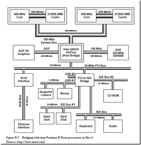
These different transfers are typically segregated onto separate busses through the use of bridges. Figure 8-7 illustrates bridging with Intel’s Pentium II Xeon processors. At the top of the diagram are two Pentium II processors, arranged in a symmetric multiprocessor (SMP) configuration. The operating system per- forms load balancing by selecting one processor over another when assigning tasks (this is different from parallel processing, discussed in Chapter 10, in which multiple processors work on a common problem.) Each Pentium II processor has a “backside bus” to its own cache of 3200 MB/sec (8 bytes wide ´ 400 MHz), thus segregating cache traffic from other bus traffic.

Working down from the top of the diagram, the two Pentium II processors converge on the System Bus (sometimes called the “frontside bus.” The System Bus is 32 bits wide and makes transfers on both the leading and falling edges of the 100 MHz bus clock, giving a total available bandwidth of 4 bytes ´ 2 edges ´ 100 MHz = 800 MB/sec that is shared between the processors.

At the center of the diagram is the Intel 440GX AGPset “Host Bridge” which connects the System Bus to the remaining busses. The Host Bridge acts as a go-between among the System Bus, the main memory, the graphics processor, and a hierarchy of other busses. To the right of the Host Bridge is the main memory (synchronous DRAM), connected to the Host Bridge by an 800 MB/sec bus.

image

In this particular example, a separate bus known as the Advanced Graphics Port (AGP) is provided from the Host Bridge to the graphics processor over a 533 MB/sec bus. Graphics rendering (that is, filling an object with color) commonly needs texture information that is too large to economically place on a graphics card. The AGP allows for a high speed path between the graphics processor and the main memory, where texture maps can now be effectively stored.

Below the Host Bridge is the 33 MHz Peripheral Component Interconnect (PCI) bus, which connects the remaining busses to the Host Bridge. The PCI bus has a number of components connected to it, such as the Small Computer System Interface (SCSI) controller which is yet another bus, that in this illustration accepts an Ethernet network interface card. Prior to the introduction of the AGP, graphics cards were placed on the PCI bus, which created a bottleneck for all of the other bus traffic.

Attached to the PCI bus is a PCI-to-ISA bridge, which actually provides bridging for two 1.5 MB/sec Universal Serial Bus (USB) busses, two 33 MB/sec integrated Drive Electronics (IDE) busses, and a 16.7 MB/sec Industry Standard Architecture (ISA) bus. The IDE busses are generally used for disk drives, the ISA bus is generally used for moderate rate devices like printers and voice-band modems, and the USB busses are used for low bit rate devices like mice and snapshot digital cameras.

8.3 Communication Methodologies

Computer systems have a wide range of communication tasks. The CPU must communicate with memory and with a wide range of I/O devices, from extremely slow devices such as keyboards, to high-speed devices like disk drives and network interfaces. There may be multiple CPUs that communicate with one another either directly or through a shared memory, as described in the previous section for the dual Pentium II Xeon configuration.

Three methods for managing input and output are programmed I/O (also known as polling), interrupt driven I/O, and direct memory access (DMA).

8.3.1 PROGRAMMED I/O

Consider reading a block of data from a disk. In programmed I/O, the CPU polls each device to see if it needs servicing. In a restaurant analogy, the host would approach the patron and ask if the patron is ready.

The operations that take place for programmed I/O are shown in the flowchart in Figure 8-8. The CPU first checks the status of the disk by reading a special register that can be accessed in the memory space, or by issuing a special I/O instruction if this is how the architecture implements I/O. If the disk is not ready to be read or written, then the process loops back and checks the status continuously until the disk is ready. This is referred to as a busy-wait. When the disk is finally ready, then a transfer of data is made between the disk and the CPU.

After the transfer is completed, the CPU checks to see if there is another communication request for the disk. If there is, then the process repeats, otherwise the CPU continues with another task.

image

In programmed I/O the CPU wastes time polling devices. Another problem is that high priority devices are not checked until the CPU is finished with its cur- rent I/O task, which may have a low priority. Programmed I/O is simple to implement, however, and so it has advantages in some applications.

8.3.2 INTERRUPT-DRIVEN I/O

With interrupt driven I/O, the CPU does not access a device until it needs servicing, and so it does not get caught up in busy-waits. In interrupt-driven I/O, the device requests service through a special interrupt request line that goes directly to the CPU. The restaurant analogy would have the patron politely tap- ping silverware on a water glass, thus interrupting the waiter when service is required.

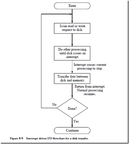
A flowchart for interrupt driven I/O is shown in Figure 8-9. The CPU issues a

image

request to the disk for reading or for writing, and then immediately resumes execution of another process. At some later time, when the disk is ready, it interrupts the CPU. The CPU then invokes an interrupt service routine (ISR) for the disk, and returns to normal execution when the interrupt service routine completes its task. The ISR is similar in structure to the procedure presented in Chapter 4, except that interrupts occur asynchronously with respect to the process being executed by the CPU: an interrupt can occur at any time during pro- gram execution.

There are times when a process being executed by the CPU should not be interrupted because some critical operation is taking place. For this reason, instruction sets include instructions to disable and enable interrupts under programmed control. (The waiter can ignore the patron at times.) Whether or not interrupts are accepted is generally determined by the state of the Interrupt Flag (IF) which is part of the Processor Status Register. Furthermore, in most systems priorities are assigned to the interrupts, either enforced by the processor or by a peripheral interrupt controller (PIC). (The waiter may attend to the head table first.) At the top priority level in many systems, there is a non maskable interrupt (NMI) which, as the name implies, cannot be disabled. (The waiter will in all cases pay attention to the fire alarm!) The NMI is used for handling potentially catastrophic events such as power failures, and more ordinary but crucially uninterruptible operations such as file system updates.

At the time when an interrupt occurs (which is sometimes loosely referred to as a trap, even though traps usually have a different meaning, as explained in Chapter 6), the Processor Status Register and the Program Counter (%psr and %pc for the ARC) are automatically pushed onto the stack, and the Program Counter is loaded with the address of the appropriate interrupt service routine. The processor status register is pushed onto the stack because it contains the interrupt flag (IF), and the processor must disable interrupts for at least the duration of the first instruction of the ISR. (See problem 8.2.) Execution of the interrupt routine then begins. When the interrupt service routine finishes, execution of the interrupted program then resumes.

The ARC jmpl instruction (see Chapter 4) will not work properly for resuming execution of the interrupted routine, because in addition to restoring the pro- gram counter contents, the processor status register must be restored. Instead, the rett (return from trap) instruction is invoked, which reverses the interrupt process and restores the %psr and %pc registers to their values prior to the interrupt. In the ARC architecture, rett is an arithmetic format instruction with op3 = 111001, and an unused rd field (all zeros).

8.3.3 DIRECT MEMORY ACCESS (DMA)

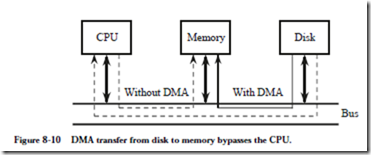
Although interrupt driven I/O frees the CPU until the device requires service, the CPU is still responsible for making the actual data transfer. Figure 8-10 high-

image

lights the problem. In order to transfer a block of data between the memory and the disk using either programmed I/O or interrupt driven I/O, every word travels over the system bus (or equivalently, through the Host Bridge) twice: first to the CPU, then again over the system bus to its destination.

A DMA device can transfer data directly to and from memory, rather than using the CPU as an intermediary, and can thus relieve congestion on the system bus. In keeping with the restaurant analogy, the host serves everyone at one table before serving anyone at another table. DMA services are usually provided by a DMA controller, which is itself a specialized processor whose specialty is transfer- ring data directly to or from I/O devices and memory. Most DMA controllers can also be programmed to make memory-to-memory block moves. A DMA device thus takes over the job of the CPU during a transfer. In setting up the transfer, the CPU programs the DMA device with the starting address in main memory, the starting address in the device, and the length of the block to be transferred.

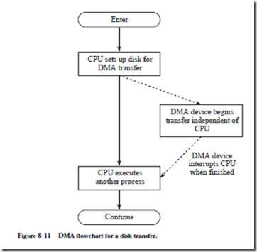
Figure 8-11 illustrates the DMA process for a disk transfer. The CPU sets up the DMA device and then signals the device to start the transfer. While the transfer is taking place, the CPU continues execution of another process. When the DMA transfer is completed, the device informs the CPU through an interrupt. A sys- tem that implements DMA thus also implements interrupts as well.

If the DMA device transfers a large block of data without relinquishing the bus, the CPU may become starved for instructions or data, and thus its work is halted until the DMA transfer has completed. In order to alleviate this problem, DMA controllers usually have a “cycle-stealing” mode. In cycle-stealing DMA the controller acquires the bus, transfers a single byte or word, and then relinquishes the bus. This allows other devices, and in particular the CPU, to share the bus during DMA transfers. In the restaurant analogy, a patron can request a check while the host is serving another table.
image


Input and output: simple bus architectures ( bus structure, protocol, and control, bus clocking, the synchronous bus, the asynchronous bus and bus arbitration—masters and slaves).

INPUT AND OUTPUT

In the earlier chapters, we considered how the CPU interacts with data that is accessed internal to the CPU, or is accessed within the main memory, which may be extended to a hard magnetic disk through virtual memory. While the access speeds at the different levels of the memory hierarchy vary dramatically, for the most part, the CPU sees the same response rate from one access to the next. The situation when accessing input/output (I/O) devices is very different.

• The speeds of I/O data transfers can range from extremely slow, such as reading data entered from a keyboard, to so fast that the CPU may not be able to keep up, as may be the case with data streaming from a fast disk drive, or real time graphics being written to a video monitor.

• I/O activities are asynchronous, that is, not synchronized to the CPU clock, as are memory data transfers. Additional signals, called handshaking signals, may need to be incorporated on a separate I/O bus to coordinate when the device is ready to have data read from it or written to it.

• The quality of the data may be suspect. For example, line noise during data transfers using the public switched telephone network, or errors caused by media defects on disk drives mean that error detection and correction strategies may be needed to ensure data integrity.

• Many I/O devices are mechanical, and are in general more prone to failure than the CPU and main memory. A data transfer may be interrupted due to mechanical failure, or special conditions such as a printer being out of paper, for example.

• I/O software modules, referred to as device drivers, must be written in such a way as to address the issues mentioned above.

In this chapter we discuss the nature of communicating using busses, starting

first with simple bus fundamentals and then exploring multiple-bus architectures. We then take a look at some of the more common I/O devices that are connected to these busses.

In the next sections we discuss communications from the viewpoints of communications at the CPU and motherboard level, and then branch out to the local area network.

8.1 Simple Bus Architectures

A computer system may contain many components that need to communicate with each other. In a worst case scenario, all N components need to simultaneously communicate with every other component, in which N2/2 links are needed for N components. The number of links becomes prohibitively large for even small values of N, but fortunately, as for long distance telecommunication, not all devices need to simultaneously communicate.

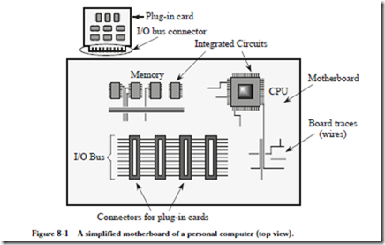
A bus is a common pathway that connects a number of devices. An example of a bus can be found on the motherboard (the main circuit board that contains the central processing unit) of a personal computer, as illustrated in simplified form in Figure 8-1. (For a look at a real motherboard, see Figure 1-6.) A typical moth-

image

erboard contains integrated circuits (ICs) such as the CPU chip and memory

chips, board traces (wires) that connect the chips, and a number of busses for chips or devices that need to communicate with each other. In Figure 8-1, an I/O bus is used for a number of cards that plug into the connectors, perpendicular to the motherboard in this example configuration.

8.1.1 BUS STRUCTURE, PROTOCOL, AND CONTROL

A bus consists of the physical parts, like connectors and wires, and a bus proto- col. The wires can be partitioned into separate groups for control, address, data, and power as illustrated in Figure 8-2. A single bus may have a few different

image

power lines, and the example shown in Figure 8-2 has lines for ground (GND) at 0 V, and positive and negative voltages at +5 V, and –15 V, respectively.

The devices share a common set of wires, and only one device may send data at any one time. All devices simultaneously listen, but normally only one device receives. Only one device can be a bus master, and the remaining devices are then considered to be slaves. The master controls the bus, and can be either a sender or a receiver.

An advantage of using a bus is to eliminate the need for connecting every device with every other device, which avoids the wiring complexity that would quickly dominate the cost of such a system. Disadvantages of using a bus include the slowdown introduced by the master/slave configuration, the time involved in implementing a protocol (see below), and the lack of scalability to large sizes due to fan-out and timing constraints.

A bus can be classified as one of two types: synchronous or asynchronous. For a synchronous bus, one of the devices that is connected to the bus contains an oscillator (a clock) that sends out a sequence of 1’s and 0’s at timed intervals as illustrated in Figure 8-3. The illustration shows a train of pulses that repeat at 10 ns intervals, which corresponds to a clock rate of 100 MHz. Ideally, the clock

image

would be a perfect square wave (instantaneous rise and fall times) as shown in the figure. In practice, the rise and fall times are approximated by a rounded, trapezoidal shape.

8.1.2 BUS CLOCKING

For a synchronous bus, discussed below, a clock signal is used to synchronize bus operations. This bus clock is generally derived from the master system clock, but it may be slower than the master clock, especially in higher-speed CPUs. For example, one model of the Power Macintosh G3 computer has a system clock speed of 333 MHz, but a bus clock speed of 66 MHz, which is slower by a factor of 5. This corresponds with memory access times which are much longer than internal CPU clock speeds. Typical cache memory has an access time of around 20 ns, compared to a 3 ns clock period for the processor described above.

In addition to the bus clock running at a slower speed than the processor, several bus clock cycles are usually required to effect a bus transaction, referred to collectively as a single bus cycle. Typical bus cycles run from two to five bus clock periods in duration.

8.1.3 THE SYNCHRONOUS BUS

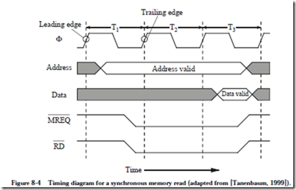
As an example of how communication takes place over a synchronous bus, con- sider the timing diagram shown in Figure 8-4 which is for a synchronous read of a word of memory by a CPU. At some point early in time interval T1, while the clock is high, the CPU places the address of the location it wants to read onto the address lines of the bus. At some later time during T1, after the voltages on the address lines have become stable, or “settled,” the imageand RD lines are asserted by the CPU.

imageinforms the memory that it is selected for the transfer (as opposed to another device, like a disk). The RD line informs the selected device to perform a read operation. The overbars onimageand RD indicate that a 0 must be placed on these lines in order to assert them.

image

The read time of memory is typically slower than the bus speed, and so all of time interval T2 is spent performing the read, as well as part of T3. The CPU assumes a fixed read time of three bus clocks, and so the data is taken from the bus by the CPU during the third cycle. The CPU then releases the bus by de-asserting MREQ and RD in T3. The shaded areas of the data and address portions of the timing diagram indicate that these signals are either invalid or unimportant at those times. The open areas, such as for the data lines during T3, indicate valid signals. Open and shaded areas are used with crossed lines at either end to indicate that the levels of the individual lines may be different.

8.1.4 THE ASYNCHRONOUS BUS

If we replace the memory on a synchronous bus with a faster memory, then the memory access time will not improve because the bus clock is unchanged. If we increase the speed of the bus clock to match the faster speed of the memory, then slower devices that use the bus clock may not work properly.

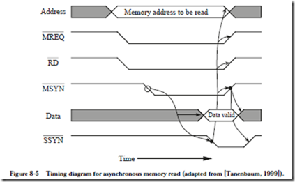
An asynchronous bus solves this problem, but is more complex, because there is no bus clock. A master on an asynchronous bus puts everything that it needs on the bus (address, data, control), and then asserts  MSYN (master synchronization). The slave then performs its job as quickly as it can, and then asserts SSYN (slave synchronization) when it is finished. The master then de-asserts MSYN , which signals the slave to de-assert SSYN . In this way, a fast master/slave combination responds more quickly than a slow master/slave combination.

As an example of how communication takes place over an asynchronous bus, consider the timing diagram shown in Figure 8-5. In order for a CPU to read a

image

word from memory, it places an address on the bus, followed by asserting MREQ and RD . After these lines settle, the CPU asserts MSYN . This event triggers the memory to perform a read operation, which results in SSYN eventually being asserted by the memory. This is indicated by the cause-and-effect arrow between MSYN and SSYN shown in Figure 8-5. This method of synchronization is referred to as a “full handshake.” In this particular implementation of a full handshake, asserting MSYN initiates the transfer, followed by the slave asserting SSYN , followed by the CPU de-asserting MSYN , followed by the memory de-asserting SSYN . Notice the absence of a bus clock signal.

Asynchronous busses can be more difficult to debug than synchronous busses when there is a problem, and interfaces for asynchronous busses can be more difficult to make. For these reasons, synchronous busses are very common, particularly in personal computers.

8.1.5 BUS ARBITRATION—MASTERS AND SLAVES

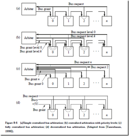
Suppose now that more than one device wants to be a bus master at the same time. How is a decision made as to who will be the bus master? This is the bus arbitration problem, and there are two basic schemes: centralized and decentralized (distributed). Figure 8-6 illustrates four organizations for these two

image

schemes. In Figure 8-6a, a centralized arbitration scheme is used. Devices 0 through n are all attached to the same bus (not shown), and they also share a bus request line that goes into an arbiter. When a device wants to be a bus master, it asserts the bus request line. When the arbiter sees the bus request, it determines if a bus grant can be issued (it may be the case that the current bus master will not allow itself to be interrupted). If a bus grant can be issued, then the arbiter asserts the bus grant line. The bus grant line is daisy chained from one device to the next. The first device that sees the asserted bus grant and also wants to be the bus master takes control of the bus and does not propagate the bus grant to higher

numbered devices. If a device does not want the bus, then it simply passes the bus grant to the next device. In this way, devices that are electrically closer to the arbiter have higher priorities than devices that are farther away.

Sometimes an absolute priority ordering is not appropriate, and a number of bus request/bus grant lines are used as shown in Figure 8-6(b). Lower numbered bus request lines have higher priorities than higher numbered bus request lines. In order to raise the priority of a device that is far from the arbiter, it can be assigned to a lower numbered bus request line. Priorities are assigned within a group on the same bus request level by electrical proximity to the arbiter.

Taking this to an extreme, each device can have its own bus request/bus grant line as shown in Figure 8-6(c). This fully centralized approach is the most powerful from a logical standpoint, but from a practical standpoint, it is the least scalable of all of the approaches. A significant cost is the need for additional lines (a precious commodity) on the bus.

In a fourth approach, a decentralized bus arbitration scheme is used as illustrated in Figure 8-6(d). Notice the lack of a central arbiter. A device that wants to become a bus master first asserts the bus request line, and then it checks if the bus is busy. If the busy line is not asserted, then the device sends a 0 to the next higher numbered device on the daisy chain, asserts the busy line, and de-asserts the bus request line. If the bus is busy, or if a device does not want the bus, then it simply propagates the bus grant to the next device.

Arbitration needs to be a fast operation, and for that reason, a centralized scheme will only work well for a small number of devices (up to about eight). For a large number of devices, a decentralized scheme is more appropriate.

Given a system that makes use of one of these arbitration schemes, imagine a situation in which n card slots are used, and then card m is removed, where m < n. What happens? Since each bus request line is directly connected to all devices in a group, and the bus grant line is passed through each device in a group, a bus request from a device with an index greater than m will never see an asserted bus grant line, which can result in a system crash. This can be a frustrating problem to identify, because a system can run indefinitely with no problems, until the higher numbered device is accessed.

When a card is removed, higher cards should be repositioned to fill in the missing slot, or a dummy card that continues the bus grant line should be inserted in

place of the removed card. Fast devices (like disk controllers) should be given higher priority than slow devices (like terminals), and should thus be placed close to the arbiter in a centralized scheme, or close to the beginning of the Bus grant line in a decentralized scheme. This is an imperfect solution given the opportunities for leaving gaps in the bus and getting the device ordering wrong. These days, it is more common for each device to have a separate path to the arbiter.


SUMMARY OF MEMORY

■ SUMMARY

Memory is organized in a hierarchy in which the densest memory offers the least performance, whereas the greatest performance is realized with the memory that has the least density. In order to bridge the gap between the two, the principle of locality is exploited in cache and virtual memories.

A cache memory maintains the most frequently used blocks in a small, fast memory that is local to the CPU. A paged virtual memory augments a main memory with disk storage. The physical memory serves as a window on the paged virtual memory, which is maintained in its entirety on a hard magnetic disk.

Cache and paged virtual memories are commonly used on the same computer, but for different reasons. A cache memory improves the average access time to the main memory, whereas a paged virtual memory extends the size of the main memory.

In an example memory architecture, the Intel Pentium has a split L1 cache and a TLB that reside on the Pentium core, and a unified L2 cache that resides in the same package as the Pentium although on a different silicon die. When paging is implemented, the page table is located in main memory, with the TLB reducing the number of times that the TLB is referenced. The L1 and L2 cache memories then reduce the number of times main memory is accessed for data. The Pentium also supports segmentation, which has its own set of mapping registers and control hardware that resides on the Pentium.

■ FURTHER READING

(Stallings, 1993) and (Mano, 1991) give readable explanations of RAM. A number of memory databooks (Micron, 1992) and (Texas Instruments, 1991) give practical examples of memory organization. (Foster, 1976) is the seminal reference on CAM. (Mead and Conway, 1980) describe the H-tree structure in the context of VLSI design. (Franklin et al, 1982) explores issues in partitioning chips, which arise in splitting an H-tree for a CAM. (Sedra and Smith, 1997) discuss the implementation of several kinds of static and dynamic RAM.

(Hamacher et al, 1990) gives a classic treatment of cache memory. (Tanenbaum, 1990) gives a readable explanation of virtual memory. (Hennessy and Patterson, 1995) and (Przybylski, 1990) cover issues relating to cache performance. Seg- mentation on the Intel Pentium processor is covered in (Intel, 1993). Kingston Technology gives a broad tutorial on memory technologies at http://www.king- ston.com/king/mg0.htm.

Foster, C. C., Content Addressable Parallel Processors, Van Nostrand Reinhold Company, (1976).

Franklin, M. A., D. F. Wann, and W. J. Thomas, “Pin Limitations and Partitioning of VLSI Interconnection Networks,” IEEE Trans Comp., C-31, 1109, (Nov. 1982).

Hamacher, V. C., Z. G. Vranesic, and S. G. Zaky, Computer Organization, 3/e, McGraw Hill, (1990).

Hennessy, J. L. and D. A. Patterson, Computer Architecture: A Quantitative Approach, 2/e, Morgan Kaufmann Publishers, San Mateo, California, (1995).

Intel Corporation, Pentium Processor User’s Manual, Volume 3: Architecture and Programming Manual, (1993).

Knuth, D., The Art of Computer Programming: Fundamental Algorithms, vol. 1, 2/e, Addison-Wesley, (1974).

Mano, M., Digital Design, 2/e, Prentice Hall, (1991).

Mead, C. and L. Conway, Introduction to VLSI Systems, Addison Wesley, (1980). Micron, DRAM Data Book, Micron Technologies, Inc., 2805 East Columbia Road, Boise, Idaho, (1992).

Przybylski, S. A., Cache and Memory Hierarchy Design, Morgan Kaufmann Publishers, (1990).

Sedra, A., and Smith, K., Microelectronic Circuits, 4/e, Oxford University Press, New York, (1997).

Stallings, W., Computer Organization and Architecture, 3/e, MacMillan Publishing, New York, (1993).

Tanenbaum, A., Structured Computer Organization, 3/e, Prentice Hall, Englewood Cliffs, New Jersey, (1990).

Texas Instruments, MOS Memory: Commercial and Military Specifications Data Book, Texas Instruments, Literature Response Center, P.O. Box 172228, Denver, Colorado, (1991).

PROBLEMS

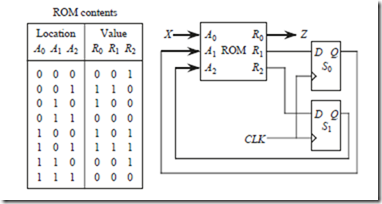
7.1 A ROM lookup table and two D flip-flops implement a state machine as shown in the diagram below. Construct a state table that describes the machine.

image

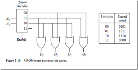
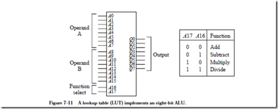
7.2 Fill in four memory locations for the lookup table shown in Figure 7-11 in which each of the four operations: add, subtract, multiply, and divide are performed on A=16 and B=4. Show the address and the value for each case.

7.3 Design an eight-word, 32-bit RAM using 8´8 RAMs.

7.4 Design a 16-word, four-bit RAM using 4´4 RAMs and a single external decoder.

7.5 Given a number of n-word by p-bit RAM chips:

(a) Show how to construct an n-word ´ 4p-bit RAM using these chips. Use any other logic components that you have seen in the text that you feel are needed.

(b) Show how to construct a 4n-word ´ p-bit RAM using these chips.

7.6 Draw the circuit for a 4-to-16 tree decoder, using a maximum fan in and fan-out of two.

7.7 A direct mapped cache consists of 128 slots. Main memory contains 16K blocks of 16 words each. Access time of the cache is 10 ns, and the time required to fill a cache slot is 200 ns. Load-through is not used; that is, when an accessed word is not found in the cache, the entire block is brought into the cache, and the word is then accessed through the cache. Initially, the cache is empty. Note: When referring to memory, 1K = 1024.

(a) Show the format of the memory address.

(b) Compute the hit ratio for a program that loops 10 times from locations 15 – 200. Note that although the memory is accessed twice during a miss (once for the miss, and once again to satisfy the reference), a hit does not occur for this case. To a running program, only a single memory reference is observed.

(c) Compute the effective access time for this program.

7.8 A fully associative mapped cache has 16 blocks, with eight words per block. The size of main memory is 216 words, and the cache is initially empty. Access time of the cache is 40 ns, and the time required to transfer eight words between main memory and the cache is 1 µs.

(a) Compute the sizes of the tag and word fields.

(b) Compute the hit ratio for a program that executes from 20–45, then loops four times from 28–45 before halting. Assume that when there is a miss, that the entire cache slot is filled in 1 µs, and that the first word is not seen by the CPU until the entire slot is filled. That is, assume load-through is not used. Initially, the cache is empty.

(c) Compute the effective access time for the program described in part (b) above.

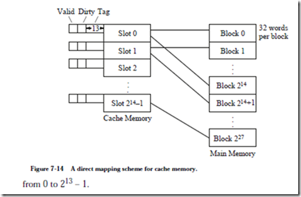
7.9 Compute the total number of bits of storage needed for the associative mapped cache shown in Figure 7-13 and the direct mapped cache shown in Figure 7-14. Include Valid, Dirty, and Tag bits in your count. Assume that the word size is eight bits.

7.10 (a) How far apart do memory references need to be spaced to cause a miss on every cache access using the direct mapping parameters shown in Figure 7-14?

(b) Using your solution for part (a) above, compute the hit ratio and effective access time for that program with TMiss = 1000 ns, and THit = 10 ns. Assume that load-through is used.

7.11 A computer has 16 pages of virtual address space but only four physical page frames. Initially the physical memory is empty. A program references the virtual pages in the order: 0 2 4 5 2 4 3 11 2 10.

(a) Which references cause a page fault with the LRU page replacement pol- icy?

(b) Which references cause a page fault with the FIFO page replacement pol- icy?

7.12 On some computers, the page table is stored in memory. What would happen if the page table is swapped out to disk? Since the page table is used for every memory reference, is there a page replacement policy that guarantees that the page table will not get swapped out? Assume that the page table is small enough to fit into a single page (although usually it is not).

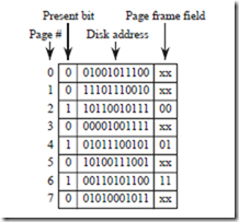
7.13 A virtual memory system has a page size of 1024 words, eight virtual pages, four physical page frames, and uses the LRU page replacement policy. The page table is as follows:

image

(a) What is the main memory address for virtual address 4096?

(b) What is the main memory address for virtual address 1024?

(c) A fault occurs on page 0. Which page frame will be used for virtual page 0?

7.14 When running a particular program with N memory accesses, a computer with a cache and paged virtual memory generates a total of M cache misses and F page faults. T1 is the time for a cache hit; T2 is the time for a main memory hit; and T3 is the time to load a page into main memory from the disk.

(a) What is the cache hit ratio?

(b) What is the main memory hit ratio? That is, what percentage of main memory accesses do not generate a page fault?

(c) What is the overall effective access time for the system?

7.15 A computer contains both cache and paged virtual memories. The cache can hold either physical or virtual addresses, but not both. What are the issues involved in choosing between caching virtual or physical addresses? How can these problems be solved by using a single unit that manages all memory map- ping functions?

7.16 How much storage is needed for the page table for a virtual memory that has 232 bytes, with 212 bytes per page, and 8 bytes per page table entry?

7.17 Compute the gate input count for the decoder(s) of a 64 ´ 1-bit RAM for both the 2D and the 2-1/2D cases. Assume that an unlimited fan-in/fan-out is allowed. For both cases, use ordinary two-level decoders. For the 2 1/2D case, treat the column decoder as an ordinary MUX. That is, ignore its behavior as a DEMUX during a write operation.

7.18 How many levels of decoding are needed for a 220 word 2D memory if a fan-in of four and a fan-out of four are used in the decoder tree?

7.19 A video game cartridge needs to store 220 bytes in a ROM.

(a) If a 2D organization is used, how many leaves will be at the deepest level of the decoder tree?

(b) How many leaves will there be at the deepest level of the decoder tree for a 2-1/2D organization?

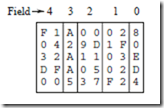
7.20 The contents of a CAM are shown below. Which set of words will respond if a key of 00A00020 is used on fields 1 and 3? Fields 1 and 3 of the key must match the corresponding fields of a CAM word in order for that word to respond. The remaining fields are ignored during the matching process but are included in the retrieved words.

image

7.21 When the TLB shown in Figure 7-27 has a miss, it accesses the page table to resolve the reference. How many entries are in that page table?


Memory: case study: ramous memory and case study: the Intel Pentium memory system.

Case Study: Rambus Memory

There was a time when computer technology would be pushed from the laboratory into the marketplace. As the consumer marketplace for computing devices exploded, the “technology push” was replaced by “market pull,” and consumer demand then dominated the preferences of technologists when it came to developing a new memory technology. High performance, expensive memory for high-end processors was displaced by high density, low-cost memory for consumer electronics, such as videogames. It became more profitable for memory manufacturers to address the needs of high volume consumer markets, rather than devote costly chip fabrication facilities to a comparatively small high-end market.

The consumer electronics industry now dominates the memory market, and even high-end, non-consumer processors make heavy use of consumer electronics technology, exploiting architectural enhancements instead, or innovations in supporting technologies (such as high speed interconnects) to compensate for the performance shortcomings of what we might call “videogame memory.”

Videogame memory is not all that low-end, however, and in fact, makes use of extraordinary technology enhancements that squeeze the most performance out of ever denser, low-cost devices. A leading memory technology that is being introduced into Intel-based personal computers in 1999 was developed by Ram- bus, Inc. The Rambus DRAM (RDRAM) retrieves a block of 8 bytes internal to the DRAM chip on every access, and multiplexes the 8 bytes onto a narrow 8-bit or 16-bit channel, operating at a rate of 800 MHz (or higher).

A typical DRAM core (that is, the storage portion of an ordinary DRAM) can store or retrieve a line of 8 bytes with a 100 MHz cycle. This is internal to the DRAM chip: most DRAMs only deliver one byte per cycle, but the RDRAM technology can multiplex that up to 1 byte per cycle using a higher external clock of 800 MHz. That higher rate is fed to a memory controller (the “chipset” on an Intel machine) which demuxes it to a 32-bit wide data stream at a lower rate, such as 200 MHz, going into a Pentium (or other processor chip).

The Rambus “RIMM” modules (Rambus Inline Memory Modules) look similar to ordinary SIMMs and DIMMs, but they operate differently. The Rambus memory uses microstrip technology (also known as transmission lines) on the motherboard, which implements a crude shield that reduces radio frequency (RF) effects that interfere with data traveling through wires on the motherboard, which are called board traces. In designing a printed circuit board (PCB) for

Rambus technology, the critical parameters are (1) dielectric thickness of the PCB, (2) separation of the memory modules, and (3) trace width. There must be a ground plane (an electrical return path) beneath every signal line, with no vias (connections between board layers) along the path. All signals go on the top layer of the PCB. (A PCB can have a number of layers, typically no more than 8). The memory controller and memory modules must all be equally spaced, such as

.5 inches from the memory controller to the first RIMM, then .5 in to the next, etc.

The “Rambus Channel” is made up of transmission line traces. The trace widths end up being about twice as wide as ordinary traces, on the order of 12 mils (300 microns). Although 300 microns is relatively small for a board trace, if we want to send 128 signals over a PCB, using a 600 micron pitch (center-to-center spacing) with 300 microns between 300 micron traces, this corresponds to a foot- print of 128 ´ 600 microns = 76 mm. This is a large footprint compared with lower speed solutions that allow a much closer packing density.

In reality, the Rambus Channel only has 13 high speed signals, (the address is serialized onto a single line, there are 8 data lines, 1 parity line, 2 clock lines, and 1 command line) and so the seemingly large footprint is not a near-term problem. With a 16-bit version of the Rambus Channel on the horizon, the band- width problem appears to be in hand for a number of years using this technology. Extensibility to large word widths such as 64 bits or 128 bits will pose a significant challenge down the road, however, because the chipset will need to support that same word width – a formidable task with current packaging methods, that already have over 500 pins on the chipset.

Although Rambus memory of this type became available in 1998, the RIMM modules were not widely available until 1999, timed for the availability of a new memory controller (chipset) for the RIMMs. The memory controller is an important aspect of this type of memory because the view of memory that the CPU perceives is different from the physical memory.

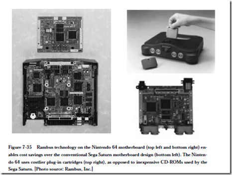
Rambus memory is more expensive than conventional DRAM memory, but overall system cost can be reduced, which makes it attractive in low-cost, high performance consumer electronics such as the Nintendo 64 video game console. The Nintendo 64 (see Figure 7-35) has four primary chips: a 64-bit MIPS RS4300i CPU; a Reality coprocessor which integrates all graphics, audio and memory management functions; and two Rambus memory chips.

image

The Rambus technology provides the Nintendo 64 with a bandwidth of 562.5 MB/s using a 31-pin interface to the memory controller. By comparison, a sys- tem using typical 64-bit-wide synchronous DRAMs (SDRAMs) requires a 110-pin interface to the memory controller. This reduction in pin count allows the memory controller to fit on the same die (the silicon chip) as the graphics and sound functions, in a relatively low-cost, 160-pin packaged chip.

The Rambus memory subsystem is made up of two memory chips which occupy 1.5 square inches of board space. An equivalent SDRAM design would require 6 square inches of board space. The space savings of using the Rambus approach enabled Nintendo to fit all of its components on a board measuring five by six inches, which is one quarter the size of the system board used in the competing Sega Saturn. In addition, Nintendo was able to use only a two-layer board instead of the four layers used in the Sega Saturn.

The cost savings Nintendo realized by choosing the Rambus solution over the 64-bit SDRAM approach are considerable, but should be placed in perspective with the overall market. The ability to use a two-layer implementation saved Nintendo $5 per unit in manufacturing costs. Taken altogether, Nintendo estimates the total bill of materials cost savings over an equivalent SDRAM-based design was about 20 percent.

These cost savings need to be placed in perspective with the marketplace, how- ever. The competing Sega Saturn and Sony Playstation use CD-ROMs for game storage, which cost under $2 each to mass produce. The Nintendo 64 uses a plug-in ROM cartridge that costs closer to $10 each to mass produce, and can only store 1% of what can be stored on a CD-ROM. This choice of media may have a great impact on the overall system architecture, and so the Rambus approach may not benefit all systems to the same degree. Details matter a great deal when it comes to evaluating the impact of a new technology on a particular market, or even a segment of a market.

Case Study: The Intel Pentium Memory System

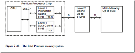
The Intel Pentium processor is typical of modern processors in its memory con- figurations. Figure 7-36 shows a simplified diagram of the memory elements and

image

data paths. There are two L1 caches on board the actual Pentium chip, an instruction, or I-cache, and a data, or D-cache. Each cache has a 256 bit (32 byte) line size, with an equally-sized data path to the CPU. The L1 caches are 2-way set associative, and each way has a single LRU bit. The D-cache can be set to write-through or writeback on a per-line basis. The D cache is write no-allocate: misses on writes do not result in a cache fill. Each cache is also equipped with a TLB that translates virtual to physical addresses. The D-cache TLB is 4-way set associative, with 64 entries, and is dual-ported, allowing two simultaneous data reference translations. The I-cache TLB is 4-way set associative with 32 entries.

The L2 cache, if present, is 2-way set associative, and can be 256 KB or 512 KB in size. The data bus, shown as “n” in the figure, can be 32, 64, or 128 bits in size.

THE MESI PROTOCOL

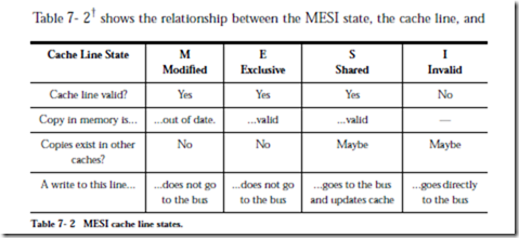
The Pentium D cache, and the L2 cache if present support the MESI cache coherency protocol for managing multiprocessor access to memory. Each D-cache line has two bits associated with it that store the MESI state. Each cache line will be in one of the four states:

• M – Modified. The contents of the cache line have been modified and are different from main memory.

• E – Exclusive. The contents of the cache line have not been modified, and are the same as the line in main memory.

• S – Shared. The line is, or may be shared with another cache line belonging to another processor.

• I – Invalid. The line is not in the cache. Reads to lines in the I state will result in cache misses.

image

the equivalent line in main memory. The MESI protocol is becoming a standard way of dealing with cache coherency in multiprocessor systems.

The Pentium processor also supports up to six main memory segments (there can be several thousand segments, but no more than 6 can be referenced through the segment registers.) As discussed in the chapter, each segment is a separate address space. Each segment has a base—a starting location within the 32-bit physical address space, and a limit, the maximum size of the segment. The limit may be either 216 bytes or 216 ´ 212 bytes in size. That is, the granularity of the limit may be one byte or 212 bytes in size.

Paging and segmentation on the Pentium can be applied in any combination:

Unsegmented, unpaged memory: The virtual address space is the same as the physical address space. No page tables or mapping hardware is needed. This is good for high performance applications that do not have a lot of complexity, that do not need to support growing tables, for example.

Unsegmented, paged memory: Same as for the unsegmented, unpaged memory above, except that the linear address space is larger as a result of using disk storage. A page table is needed to translate between virtual and physical addresses. A translation lookaside buffer is needed on the Pentium core, working in conjunction with the L1 cache, to reduce the number of page table accesses.

Segmented, unpaged memory: Good for high complexity applications that need to support growing data structures. This is also fast: segments are fewer in number than pages in a virtual memory, and all of the segmentation mapping hardware typically fits on the CPU chip. There is no need for disk accesses as there would be for paging, and so access times are more predictable than when paging is used.

Segmented, paged memory: A page table, segment mapping registers, and TLB all work in conjunction to support multiple address spaces.

Segmentation on the Intel Pentium processor is quite powerful but is also quite complex. We only explore the basics here, and the interested reader is referred to (Intel, 1993) for a more complete description.


Memory: advanced topics (tree decoders, decoders for large rams and content-addressable (associative) memories).

Advanced Topics

This section covers two topics that are of practical importance in designing memory systems: tree decoders and content-addressable memories. The former are required in large memories. The latter are required for associative caches, such as a TLB, or in other situations when data must be looked up at high speed based on its value, rather than on the address of where it is stored.

TREE DECODERS

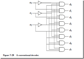
Decoders (see Appendix A) do not scale well to large sizes due to practical limitations on fan-in and fan-out. The decoder circuit shown in Figure 7-28 illustrates

image

the problem. For N address bits, every AND gate has a fan-in of N. Each address line is fanned out to 2N AND gates. The circuit depth is two gates.

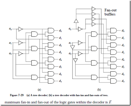
The circuit shown in Figure 7-29a is a tree decoder, which reduces the fan-in and fan-out by increasing circuit depth. For this case, each AND gate has a fan-in of F (for this example, F = 2) and only the address line that is introduced at the deepest level (a0 here) is fanned out to 2N/2 AND gates. The depth has now increased to logF(2N). The large fan-out for the higher order address bits may be a problem, but this can be easily fixed without increasing the circuit depth by adding fan-out buffers in the earlier levels, as shown in Figure 7-29b.

Thus, the depth of a memory decoder tree is logF(2N), the width is 2N, and the

image

DECODERS FOR LARGE RAMS

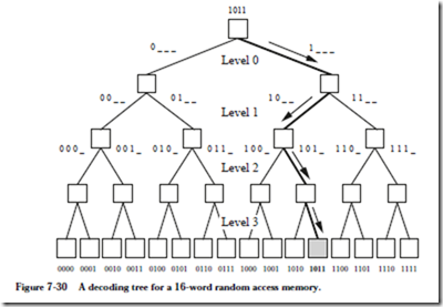
For very large RAMs, if the 2-1/2D decoding scheme is not used, tree decoders are employed to keep fanin and fanout to manageable levels. In a conventional RAM an M-bit wide address uniquely identifies one memory location out of a memory space of 2M locations. In order to access a particular location, an address is presented to the root of a decoder tree containing M levels and 2M leaves. Starting with the root (the top level of the tree) a decision is made at each ith level of the tree, corresponding to the ith bit of the address. If the ith bit is 0 at the ith level, then the tree is traversed to the left, otherwise the tree is traversed to the right. The target leaf is at level M – 1 (counting starts at 0). There is exactly one leaf for each memory address.

The tree structure results in an access time that is logarithmic in the size of the memory. That is, if a RAM contains N words, then the memory can be accessed in OélogFNù time, where F is the fan-out of the logic gates in the decoder tree (here, we assume a fan-out of two). For a RAM of size N, M = élogFNù address bits are needed to uniquely identify each word. As the number of words in the memory grows, the length of the address grows logarithmically, so that one level of depth is added to the decoder tree each time the size of the memory doubles. As a practical example, consider a 128 megaword memory that requires 27 levels of decoding (227 = 128 Mwords). If we assume that logic gates in the decoding tree switch in 2 ns, then an address can be decoded in 54 ns.

A four level decoder tree for a 16-word RAM is shown in Figure 7-30. As an

image

example of how the decoder tree works, the address 1011 is presented at the root node. The most significant bit in the address is a 1 so the right path is traversed at Level 0 as indicated by the arrow. The next most significant bit is a 0 so the left path is traversed at Level 1, the next bit is a 1 so the right path is traversed at Level 2, and the least significant bit is a 1 so the rightmost path is traversed next and the addressed leaf is then reached at Level 3.

CONTENT-ADDRESSABLE (ASSOCIATIVE) MEMORIES

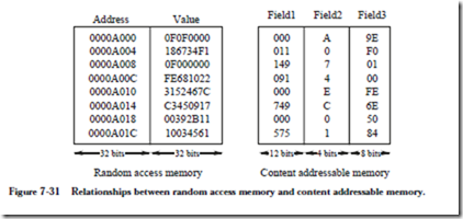
In an ordinary RAM, an address is applied to the memory, and the contents of the given location are either read or written. In a content-addressable memory (CAM), also known as an associative memory, a word composed of fields is applied to the memory and the resulting address (or index) is returned if the word or field is present in the memory. The physical location of a CAM word is generally not as significant as the values contained in the fields of the word. Relationships between addresses, values, and fields for RAM and CAM are shown in Figure 7-31.

image

Values are stored in sequential locations in a RAM, with an address acting as the key to locate a word. Four-byte address increments are used in this example, in which the word size is four bytes. Values are stored in fields in the CAM, and in principle any field of a word can be used to key on the rest of the word. If the CAM words are reordered, then the contents of the CAM are virtually unchanged since physical location has no bearing on the interpretation of the fields. A reordering of the RAM may change the meanings of its values entirely. This comparison suggests that CAM may be a preferred means for storing information when there is a significant cost in maintaining data in sorted order.

When a search is made through a RAM for a particular value, the entire memory may need to be searched, one word at a time, when the memory is not sorted. When the RAM is maintained in sorted order, a number of accesses may still be required to either find the value being searched or to determine the value is not stored in the memory. In a CAM, the value being searched is broadcast to all of the words simultaneously, and logic at each word makes a field comparison for membership, and in just a few steps the answer is known. A few additional steps may be needed to collect the results but in general the time required to search a CAM is less than for a RAM in the same technology, for a number of applications.

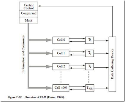
Except for maintaining tags in cache memories and in translating among net- work addresses for routing applications (see Chapter 8), CAMs are not in common use largely due to the difficulty of implementing an efficient design with conventional technology. Consider the block diagram of a CAM shown in Figure

7-32. A Central Control unit sends a comparand to each of 4096 cells, where

image

comparisons are made. The result is put in the Tag bits Ti which are collected by a Data Gathering Device and sent to the Central Control unit (Note that “Tag” is used differently here than in cache memory). When the Central Control unit loads the value to be searched into the comparand register, it sets up a mask to block out fields that are not part of the value. A small local processor in each cell makes a comparison between its local word and the broadcast value and reports the result of the comparison to the Data Gathering Device.

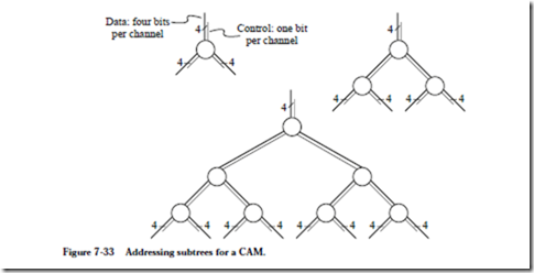
A number of problems arise when an attempt is made to implement this CAM architecture in a conventional technology such as very large scale integration (VLSI). The broadcast function that sends the comparand to the cells can be implemented with low latency if a tree structure is used. An H-tree (Mead and Conway, 1980) can be used for the tree layout if it will fit on a single IC. If the tree cannot be contained on a single chip, then connections must be made among a number of chips, which quickly limits chip density. For example, a node of a tree that has a single four-bit input and two four-bit outputs needs 12 input/output (I/O) pins and three control pins if only one node is placed on a chip. A three node subtree needs 25 pins and a seven node subtree needs 45 pins

as illustrated in Figure 7-33. A 63 node subtree requires 325 pins, excluding

image

power and control pins, which is getting close to the limit of most present day packaging technologies which do not go much higher than 1000 pins per pack- age. A useful CAM would contain thousands of such nodes with wider data paths, so the I/O bandwidth limit is realized early in the design of the CAM. Compromises can be made by multiplexing data onto the limited number of I/O connections but this reduces effective speed, which is a major reason for using a CAM in the first place.

Although implementations of CAMs are difficult, they do find practical uses, such as in TLBs and in computer networks. One application is in a network controller which receives data packets from several processors and then distributes those packets back to the processors or to other network controllers. Each processor has a unique address which the CAM keys on to determine if the target processor for a packet is in its own network or if it must be forwarded to another network.

MEMORY DESIGN EXAMPLE: A DUAL-PORT RAM

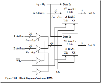
A dual-read, or dual-port RAM allows any two words to be simultaneously read from the same memory. As an example, we will design a 220 word by 8-bit dual-read RAM. For our design, any two words can be read at a time, but only one word can be written at a time. Our approach is to create two separate 220 word memories. When writing into the dual-read RAM, the address lines of both

single-read RAMs are set identically and the same data is written to both single-read memories. During a read operation, the address lines of each single-read RAM are set independently, so that two different words can be simultaneously read.

Figure 7-34 shows a block diagram for the dual-read RAM. During a write oper-

image

ation, the A address is used for both single-read RAMs. Tri-state buffers at the B RAM address inputs are controlled by the WR line. When WR=0, the A address is used at the B address input, otherwise, the B address is used at the B address input. The numbers that appear adjacent to the slashes indicate the number of individual lines that are represented by the single line. An 8 next to a slash indicates 8 lines, and a 20 next to a slash indicates 20 lines.

Each tri-state buffer has 20 input lines and 20 output lines, but Figure 7-34 uses a notation in which a single buffer represents 20 separate tri-state buffers that share the same control input. A buffer delay is inserted on the WR line in order to compensate for the delay on the complemented WR line, so that the A and B addresses are not unintentionally simultaneously enabled.


Memory: virtual memory (segmentation, fragmentation virtual memory vs, Cache memory and the translation look aside buffer).

SEGMENTATION

Virtual memory as we have discussed it up to this point is one-dimensional in the sense that addresses grow either up or down. Segmentation divides the address space into segments, which may be of arbitrary size. Each segment is its own one-dimensional address space. This allows tables, stacks, and other data structures to be maintained as logical entities that grow without bumping into each other. Segmentation allows for protection, so that a segment may be specified as “read only” to prevent changes, or “execute only” to prevent unauthorized copying. This also protects users from trying to write data into instruction areas.

When segmentation is used with virtual memory, the size of each segment’s address space can be very large, and so the physical memory devoted to each segment is not committed until needed.

Figure 7-25 illustrates a segmented memory. The executable code for a word pro-

image_thumb[5]

cessing program is loaded into Segment #0. This segment is marked as “execute only” and is thus protected from writing. Segment #1 is used for the data space for user #0, and is marked as “read/write” for user #0, so that no other user can have access to this area. Segment #2 is used for the data space for user #1, and is marked as “read/write” for user #1. The same word processor can be used by both user #0 and user #1, in which case the code in segment #0 is shared, but each user has a separate data segment.

Segmentation is not the same thing as paging. With paging, the user does not see the automatic overlaying. With segmentation, the user is aware of where segment boundaries are. The operating system manages protection and mapping, and so an ordinary user does not normally need to deal with bookkeeping, but a more sophisticated user such as a computer programmer may see the segmentation frequently when array pointers are pushed past segment boundaries in errant pro- grams.

In order to specify an address in a segmented memory, the user’s program must specify a segment number and an address within the segment. The operating sys- tem then translates the user’s segmented address to a physical address.

FRAGMENTATION

When a computer is “booted up,” it goes through an initialization sequence that loads the operating system into memory. A portion of the address space may be reserved for I/O devices, and the remainder of the address space is then available for use by the operating system. This remaining portion of the address space may be only partially filled with physical memory: the rest comprises a “Dead Zone” which must never be accessed since there is no hardware that responds to the Dead Zone addresses.

Figure 7-26a shows the state of a memory just after the initialization sequence.

image_thumb[6]

The “Free Area” is a section of memory that is available to the operating system for loading and executing programs. During the course of operation, programs of various sizes will be loaded into memory and executed. When a program finishes execution, the memory space that is assigned to that program is released to the operating system. As programs are loaded and executed, the Free Area becomes subdivided into a collection of small areas, none of which may be large enough to hold a program that would fit unless some or all of the free areas are combined into a single large area. This is a problem known as fragmentation, and is encountered with segmentation, because the segments must ultimately be mapped within a single linear address space.

Figure 7-26b illustrates the fragmentation problem. When the operating system needs to find a free area that is large enough to hold a program, it will rarely find an exact match. The free area will generally be larger than the program, which has the effect of subdividing the free areas more finely as programs are mismatched with free areas. One method of assigning programs to free areas is called first fit, in which the free areas are scanned until a large enough area is found that will satisfy the program. Another method is called best fit, in which the free area is used that wastes the least amount of space. While best fit makes better use of memory than first fit, it requires more time because all of the free areas must be scanned.

Regardless of which algorithm is used, the process of assigning programs or data to free areas tends to produce smaller free areas (Knuth, 1974). This makes it more difficult to find a single contiguous free area that is large enough to satisfy the needs of the operating system. An approach that helps to solve this problem coalesces adjacent free areas into a single larger free area. In Figure 7-26b, the two adjacent free areas are combined into a single free area, as illustrated in Figure 7-26c.

VIRTUAL MEMORY VS. CACHE MEMORY

Virtual memory is divided into pages, which are relatively large when compared with cache memory blocks, which tend to be only a few words in size. Copies of the most heavily used blocks are kept in cache memory as well as in main memory, and also in the virtual memory image that is stored on a hard disk. When a memory reference is made on a computer that contains both cache and virtual memories, the cache hardware sees the reference first and satisfies the reference if the word is in the cache. If the referenced word is not in the cache, then the block that contains the word is read into the cache from the main memory, and the referenced word is then taken from the cache. If the page that contains the word is not in the main memory, then the page is brought into the main memory from a disk unit, and the block is then loaded into the cache so that the reference can be satisfied.

The use of virtual memory causes some intricate interactions with the cache. For example, since more than one program may be using the cache and the virtual memory, the timing statistics for two runs of a program executing on the same set of data may be different. Also, when a dirty block needs to be written back to main memory, it is possible that the page frame that contains the corresponding virtual page has been overwritten. This causes the page to be loaded back to main memory from secondary memory in order to flush the dirty block from the cache memory to the main memory.

THE TRANSLATION LOOKASIDE BUFFER

The virtual memory mechanism, while being an elegant solution to the problem of accessing large programs and data files, has a significant problem associated

with it. At least two memory references are needed to access a value in memory: One reference is to the page table to find the physical page frame, and another reference is for the actual data value. The translation lookaside buffer (TLB) is a solution to this problem.

The TLB is a small associative memory typically placed inside of the CPU that stores the most recent translations from virtual to physical address. The first time a given virtual address is translated into a physical address, this translation is stored in the TLB. Each time the CPU issues a virtual address, the TLB is searched for that virtual address. If the virtual page number exists in the TLB, the TLB returns the physical page number, which can be immediately sent to the main memory (but normally, the cache memory would intercept the reference to main memory and satisfy the reference out of the cache.)

An example TLB is shown in Figure 7-27. The TLB holds 8 entries, for a system

image_thumb[7]

that has 32 pages and 16 page frames. The virtual page field is 5 bits wide because there are 25 = 32 pages. Likewise, the physical page field is 4 bits wide because there are 24=16 page frames.

TLB misses are handled in much the same way as with other memory misses. Upon a TLB miss the virtual address is applied to the virtual memory system, where it is looked up in the page table in main memory. If it is found in the page table, then the TLB is updated, and the next reference to that page will thus result in a TLB hit.


Memory: virtual memory (overlays and paging).

Virtual Memory

Despite the enormous advancements in creating ever larger memories in smaller areas, computer memory is still like closet space, in the sense that we can never have enough of it. An economical method of extending the apparent size of the main memory is to augment it with disk space, which is one aspect of virtual memory that we cover in this section. Disk storage appears near the bottom of the memory hierarchy, with a lower cost per bit than main memory, and so it is reasonable to use disk storage to hold the portions of a program or data sets that do not entirely fit into the main memory. In a different aspect of virtual memory, complex address mapping schemes are supported, which give greater flexibility in how the memory is used. We explore these aspects of virtual memory below.

OVERLAYS

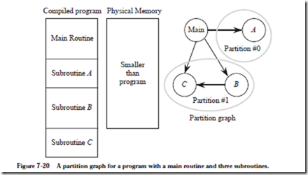
An early approach of using disk storage to augment the main memory made use of overlays, in which an executing program overwrites its own code with other code as needed. In this scenario, the programmer has the responsibility of man- aging memory usage. Figure 7-20 shows an example in which a program contains a main routine and three subroutines A, B, and C. The physical memory is smaller than the size of the program, but is larger than any single routine. A strategy for managing memory using overlays is to modify the program so that it keeps track of which subroutines are in memory, and reads in subroutine code as

image

needed. Typically, the main routine serves as the driver and manages the bulk of the bookkeeping. The driver stays in memory while other routines are brought in and out.

Figure 7-20 shows a partition graph that is created for the example program. The partition graph identifies which routines can overlay others based on which subroutines call others. For this example, the main routine is always present, and supervises which subset of subroutines are in memory. Subroutines B and C are kept in the same partition in this example because B calls C, but subroutine A is in its own partition because only the main routine calls A. Partition #0 can thus overlay partition #1, and partition #1 can overlay partition #0.

Although this method will work well in a variety of situations, a cleaner solution might be to let an operating system manage the overlays. When more than one program is loaded into memory, however, then the routines that manage the overlays cannot operate without interacting with the operating system in order to find out which portions of memory are available. This scenario introduces a great deal of complexity into managing the overlay process since there is a heavy inter- action between the operating system and each program. An alternative method that can be managed by the operating system alone is called paging, which is described in the next section.

PAGING

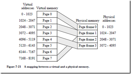
Paging is a form of automatic overlaying that is managed by the operating sys- tem. The address space is partitioned into equal sized blocks, called pages. Pages are normally an integral power of two in size such as 210 = 1024 bytes. Paging makes the physical memory appear larger than it truly is by mapping the physical memory address space to some portion of the virtual memory address space, which is normally stored on a disk. An illustration of a virtual memory mapping scheme is shown in Figure 7-21. Eight virtual pages are mapped to four physical page frames.

image

An implementation of virtual memory must handle references that are made out- side of the portion of virtual space that is mapped to physical space. The following sequence of events is typical when a referenced virtual location is not in physical memory, which is referred to as a page fault:

1) A page frame is identified to be overwritten. The contents of the page frame are written to secondary memory if changes were made to it, so that the changes are recorded before the page frame is overwritten.

2) The virtual page that we want to access is located in secondary memory and is written into physical memory, in the page frame located in (1) above.

3) The page table (see below) is updated to map the new section of virtual memory onto the physical memory.

4) Execution continues.

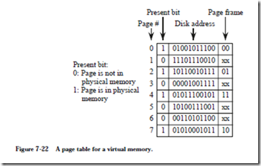
For the virtual memory shown in Figure 7-21, there are 213 = 8192 virtual locations and so an executing program must generate 13-bit addresses, which are interpreted as a 3-bit page number and a 10-bit offset within the page. Given the 3-bit page number, we need to find out where the page is: it is either in one of the four page frames, or it is in secondary memory. In order to keep track of which pages are in physical memory, a page table is maintained, as illustrated in Figure 7-22, which corresponds to the mapping shown in Figure 7-21.

image

The page table has as many entries as there are virtual pages. The present bit indicates whether or not the corresponding page is in physical memory. The disk address field is a pointer to the location that the corresponding page can be found on a disk unit. The operating system normally manages the disk accesses, and so the page table only needs to maintain the disk addresses that the operating system assigns to blocks when the system starts up. The disk addresses normally do not change during the course of computation. The page frame field indicates which physical page frame holds a virtual page, if the page is in physical memory. For pages that are not in physical memory, the page frame fields are invalid, and so they are marked with “xx” in Figure 7-22.

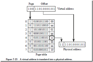
In order to translate a virtual address to a physical address, we take two page frame bits from the page table and append them to the left of the 10-bit offset, which produces the physical address for the referenced word. Consider the situation shown in Figure 7-23, in which a reference is made to virtual address 1001101000101. The three leftmost bits of the virtual address (100) identify the

image

page. The bit pattern that appears in the page frame field (11) is appended to the left of the 10-bit offset (1101000101), and the resulting address (111101000101) indicates which physical memory address holds the referenced word.

It may take a relatively long period of time for a program to be loaded into memory. The entire program may never be executed, and so the time required to load the program from a disk into the memory can be reduced by loading only the portion of the program that is needed for a given interval of time. The demand paging scheme does not load a page into memory until there is a page fault. After a program has been running for a while, only the pages being used will be in physical memory (this is referred to as the working set), so demand paging does not have a significant impact on long running programs.

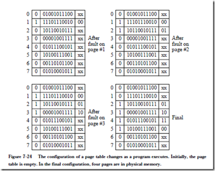
Consider again the memory mapping shown in Figure 7-21. The size of the virtual address space is 213 words, and the physical address space is 212 words. There are eight pages that each contain 210 words. Assume that the memory is initially empty, and that demand paging is used for a program that executes from memory locations 1030 to 5300. The execution sequence will make accesses to pages 1, 2, 3, 4, and 5, in that order. The page replacement policy is FIFO. Figure 7-24 shows the configuration of the page table as execution proceeds. The first access to memory will cause a page fault on virtual address 1030, which is in page #1. The page is brought into physical memory, and the valid bit and page frame field are updated in the page table. Execution continues, until page #5

image

must be brought in, which forces out page #1 due to the FIFO page replacement policy. The final configuration of the page table in Figure 7-24 is shown after location 5300 is accessed.


Memory: cache memory (set associative mapped cache, cache performance, hit ratios and effective access times, multilevel caches and cache management).

  7.6.3 SET ASSOCIATIVE MAPPED CACHE

The set associative mapping scheme combines the simplicity of direct mapping with the flexibility of associative mapping. Set associative mapping is more practical than fully associative mapping because the associative portion is limited to just a few slots that make up a set, as illustrated in Figure 7-15. For this example,

image_thumb[7]

two blocks make up a set, and so it is a two-way set associative cache. If there are four blocks per set, then it is a four-way set associative cache.

Since there are 214 slots in the cache, there are 214/2 = 213 sets. When an address is mapped to a set, the direct mapping scheme is used, and then associative map- ping is used within a set. The format for an address has 13 bits in the set field, which identifies the set in which the addressed word will be found if it is in the cache. There are five bits for the word field as before and there is a 14-bit tag field that together make up the remaining 32 bits of the address as shown below:

image_thumb[8]

As an example of how the set associative cache views a main memory address, consider again the address (A035F014)16. The leftmost 14 bits form the tag field, followed by 13 bits for the set field, followed by five bits for the word field as shown below:

image_thumb[10]

As before, the partitioning of the address field is known only to the cache, and the rest of the computer is oblivious to any address translation.

Advantages and Disadvantages of the Set Associative Mapped Cache

In the example above, the tag memory increases only slightly from the direct mapping example, to 13 ´ 214 bits, and only two tags need to be searched for each memory reference. The set associative cache is almost universally used in today’s microprocessors.

CACHE PERFORMANCE

Notice that we can readily replace the cache direct mapping hardware with associative or set associative mapping hardware, without making any other changes to the computer or the software. Only the runtime performance will change between methods.

Runtime performance is the purpose behind using a cache memory, and there are a number of issues that need to be addressed as to what triggers a word or block to be moved between the cache and the main memory. Cache read and write pol- icies are summarized in Figure 7-16. The policies depend upon whether or not the requested word is in the cache. If a cache read operation is taking place, and the referenced data is in the cache, then there is a “cache hit” and the referenced data is immediately forwarded to the CPU. When a cache miss occurs, then the entire block that contains the referenced word is read into the cache.

In some cache organizations, the word that causes the miss is immediately for- warded to the CPU as soon as it is read into the cache, rather than waiting for the remainder of the cache slot to be filled, which is known as a load-through operation. For a non-interleaved main memory, if the word occurs in the last position of the block, then no performance gain is realized since the entire slot is brought in before load-through can take place. For an interleaved main memory, the order of accesses can be organized so that a load-through operation will always result in a performance gain.

image_thumb[11]

For write operations, if the word is in the cache, then there may be two copies of the word, one in the cache, and one in main memory. If both are updated simultaneously, this is referred to as write-through. If the write is deferred until the cache line is flushed from the cache, this is referred to as write-back. Even if the data item is not in the cache when the write occurs, there is the choice of bring- ing the block containing the word into the cache and then updating it, known as write-allocate, or to update it in main memory without involving the cache, known as write-no-allocate.

Some computers have separate caches for instructions and data, which is a variation of a configuration known as the Harvard architecture (also known as a split cache), in which instructions and data are stored in separate sections of memory. Since instruction slots can never be dirty (unless we write self-modifying code, which is rare these days), an instruction cache is simpler than a data cache. In support of this configuration, observations have shown that most of the memory traffic moves away from main memory rather than toward it. Statistically, there is only one write to memory for every four read operations from memory. One reason for this is that instructions in an executing program are only read from the main memory, and are never written to the memory except by

the system loader. Another reason is that operations on data typically involve reading two operands and storing a single result, which means there are two read operations for every write operation. A cache that only handles reads, while sending writes directly to main memory can thus also be effective, although not necessarily as effective as a fully functional cache.

As to which cache read and write policies are best, there is no simple answer. The organization of a cache is optimized for each computer architecture and the mix of programs that the computer executes. Cache organization and cache sizes are normally determined by the results of simulation runs that expose the nature of memory traffic.

HIT RATIOS AND EFFECTIVE ACCESS TIMES

Two measures that characterize the performance of a cache memory are the hit ratio and the effective access time. The hit ratio is computed by dividing the number of times referenced words are found in the cache by the total number of memory references. The effective access time is computed by dividing the total time spent accessing memory (summing the main memory and cache access times) by the total

image_thumb[12]Consider computing the hit ratio and the effective access time for a program running on a computer that has a direct mapped cache with four 16-word slots. The layout of the cache and the main memory are shown in Figure 7-17. The cache access time is 80 ns, and the time for transferring a main memory block to the cache is 2500 ns. Assume that load-through is used in this architecture and that the cache is initially empty. A sample program executes from memory locations 48 – 95, and then loops 10 times from 15 – 31 before halting.

We record the events as the program executes as shown in Figure 7-18. Since the memory is initially empty, the first instruction that executes causes a miss. A miss thus occurs at location 48, which causes main memory block #3 to be read into cache slot #3. This first memory access takes 2500 ns to complete. Load-through is used for this example, and so the word that causes the miss at location 48 is passed directly to the CPU while the rest of the block is loaded into the cache

image_thumb[13]

slot. The next event consists of 15 hits for locations 49 through 63. The events that follow are recorded in a similar manner, and the result is a total of 213 hits and five misses. The total number of accesses is 213 + 5 = 218. The hit ratio and effective access time are computed as shown below:

image_thumb[14]

Although the hit ratio is 97.6%, the effective access time for this example is almost 75% longer than the cache access time. This is due to the large amount of time spent in accessing a block from main memory.

MULTILEVEL CACHES

As the sizes of silicon ICs have increased, and the packing density of components on ICs has increased, it has become possible to include cache memory on the same IC as the processor. Since the on-chip processing speed is faster than the speed of communication between chips, an on-chip cache can be faster than an off-chip cache. Current technology is not dense enough to allow the entire cache to be placed on the same chip as the processor, however. For this reason, multilevel caches have been developed, in which the fastest level of the cache, L1, is on the same chip as the processor, and the remaining cache is placed off of the processor chip. Data and instruction caches are separately maintained in the L1 cache. The L2 cache is unified, which means that the same cache holds both data and instructions.

In order to compute the hit ratio and effective access time for a multilevel cache, the hits and misses must be recorded among both caches. Equations that represent the overall hit ratio and the overall effective access time for a two-level cache are shown below. H1 is the hit ratio for the on-chip cache, H2 is the hit ratio for the off-chip cache, and TEFF is the overall effective access time. The method can be extended to any number of levels.

image_thumb[15]

CACHE MANAGEMENT

Management of a cache memory presents a complex problem to the system programmer. If a given memory location represents an I/O port, as it may in memory-mapped systems, then it probably should not appear in the cache at all. If it is cached, the value in the I/O port may change, and this change will not be reflected in the value of the data stored in the cache. This is known as “stale”

data: the copy that is in the cache is “stale” compared with the value in main memory. Likewise, in shared-memory multiprocessor environments (see Chapter 10), where more than one processor may access the same main memory, either the cached value or the value in main memory may become stale due to the activity of one or more of the CPUs. At a minimum, the cache in a multiprocessor environment should implement a write-through policy for those cache lines which map to shared memory locations.

For these reasons, and others, most modern processor architectures allow the sys- tem programmer to have some measure of control over the cache. For example, the Motorola PPC 601 processor’s cache, which normally enforces a write-back policy, can be set to a write-through policy on a per-line basis. Other instructions allow individual lines to be specified as noncacheable, or to be marked as invalid, loaded, or flushed.

Internal to the cache, replacement policies (for associative and set-associative caches) need to be implemented efficiently. An efficient implementation of the LRU replacement policy can be achieved with the Neat Little LRU Algorithm (origin unknown). Continuing with the cache example used in Section 7.6.5, we construct a matrix in which there is a row and a column for every slot in the cache, as shown in Figure 7-19. Initially, all of the cells are set to 0. Each time

image_thumb[16]

that a slot is accessed, 1’s are written into each cell in the row of the table that

corresponds to that slot. 0’s are then written into each cell in the column that corresponds to that slot. Whenever a slot is needed, the row that contains all 0’s is the oldest and is used next. At the beginning of the process, more than one row will contain all 0’s, and so a tie-breaking mechanism is needed. The first row with all 0’s is one method that will work, which we use here.

The example shown in Figure 7-19 shows the configuration of the matrix as blocks are accessed in the order: 0, 2, 3, 1, 5, 4. Initially, the matrix is filled with 0’s. After a reference is made to block 0, the row corresponding to block 0 is filled with 1’s and the column corresponding to block 0 is filled with 0’s. For this example, block 0 happens to be placed in slot 0, but for other situations, block 0 can be placed in any slot. The process continues until all cache slots are in use at the end of the sequence: 0, 2, 3, 1. In order to bring the next block (5) into the cache, a slot must be freed. The row for slot 0 contains 0’s, and so it is the least recently used slot. Block 5 is then brought into slot 0. Similarly, when block 4 is brought into the cache, slot 2 is overwritten.


Memory: cache memory (associative mapped cache and direct mapped cache).

Cache Memory

When a program executes on a computer, most of the memory references are made to a small number of locations. Typically, 90% of the execution time of a program is spent in just 10% of the code. This property is known as the locality principle. When a program references a memory location, it is likely to reference that same memory location again soon, which is known as temporal locality. Similarly, there is spatial locality, in which a memory location that is near a recently referenced location is more likely to be referenced than a memory location that is farther away. Temporal locality arises because programs spend much of their time in iteration or in recursion, and thus the same section of code is visited a disproportionately large number of times. Spatial locality arises because data tends to be stored in contiguous locations. Although 10% of the code accounts for the bulk of memory references, accesses within the 10% tend to be clustered. Thus, for a given interval of time, most of memory accesses come from an even smaller set of locations than 10% of a program’s size.

Memory access is generally slow when compared with the speed of the central processing unit (CPU), and so the memory poses a significant bottleneck in computer performance. Since most memory references come from a small set of locations, the locality principle can be exploited in order to improve performance. A small but fast cache memory, in which the contents of the most commonly accessed locations are maintained, can be placed between the main memory and the CPU. When a program executes, the cache memory is searched first, and the referenced word is accessed in the cache if the word is present. If the

referenced word is not in the cache, then a free location is created in the cache and the referenced word is brought into the cache from the main memory. The word is then accessed in the cache. Although this process takes longer than accessing main memory directly, the overall performance can be improved if a high proportion of memory accesses are satisfied by the cache.

Modern memory systems may have several levels of cache, referred to as Level 1 (L1), Level 2 (L2), and even, in some cases, Level 3 (L3). In most instances the L1 cache is implemented right on the CPU chip. Both the Intel Pentium and the IBM-Motorola PowerPC G3 processors have 32 Kbytes of L1 cache on the CPU chip.

A cache memory is faster than main memory for a number of reasons. Faster electronics can be used, which also results in a greater expense in terms of money, size, and power requirements. Since the cache is small, this increase in cost is relatively small. A cache memory has fewer locations than a main memory, and as a result it has a shallow decoding tree, which reduces the access time. The cache is placed both physically closer and logically closer to the CPU than the main memory, and this placement avoids communication delays over a shared bus.

A typical situation is shown in Figure 7-12. A simple computer without a cache

image

memory is shown in the left side of the figure. This cache-less computer contains a CPU that has a clock speed of 400 MHz, but communicates over a 66 MHz bus to a main memory that supports a lower clock speed of 10 MHz. A few bus cycles are normally needed to synchronize the CPU with the bus, and thus the difference in speed between main memory and the CPU can be as large as a factor of ten or more. A cache memory can be positioned closer to the CPU as shown in the right side of Figure 7-12, so that the CPU sees fast accesses over a 400 MHz direct path to the cache.

ASSOCIATIVE MAPPED CACHE

A number of hardware schemes have been developed for translating main memory addresses to cache memory addresses. The user does not need to know about the address translation, which has the advantage that cache memory enhancements can be introduced into a computer without a corresponding need for modifying application software.

The choice of cache mapping scheme affects cost and performance, and there is no single best method that is appropriate for all situations. In this section, an associative mapping scheme is studied. Figure 7-13 shows an associative map-

image

ping scheme for a 232 word memory space that is divided into 227 blocks of 25 = 32 words per block. The main memory is not physically partitioned in this way, but this is the view of main memory that the cache sees. Cache blocks, or cache lines, as they are also known, typically range in size from 8 to 64 bytes. Data is moved in and out of the cache a line at a time using memory interleaving (dis- cussed earlier).

The cache for this example consists of 214 slots into which main memory blocks are placed. There are more main memory blocks than there are cache slots, and any one of the 227 main memory blocks can be mapped into each cache slot (with only one block placed in a slot at a time). To keep track of which one of the 227 possible blocks is in each slot, a 27-bit tag field is added to each slot which holds an identifier in the range from 0 to 227 – 1. The tag field is the most significant 27 bits of the 32-bit memory address presented to the cache. All the tags are stored in a special tag memory where they can be searched in parallel. When- ever a new block is stored in the cache, its tag is stored in the corresponding tag memory location.

When a program is first loaded into main memory, the cache is cleared, and so while a program is executing, a valid bit is needed to indicate whether or not the slot holds a block that belongs to the program being executed. There is also a dirty bit that keeps track of whether or not a block has been modified while it is in the cache. A slot that is modified must be written back to the main memory before the slot is reused for another block.

A referenced location that is found in the cache results in a hit, otherwise, the result is a miss. When a program is initially loaded into memory, the valid bits are all set to 0. The first instruction that is executed in the program will therefore cause a miss, since none of the program is in the cache at this point. The block that causes the miss is located in the main memory and is loaded into the cache.

In an associative mapped cache, each main memory block can be mapped to any slot. The mapping from main memory blocks to cache slots is performed by partitioning an address into fields for the tag and the word (also known as the “byte” field) as shown below:

image

When a reference is made to a main memory address, the cache hardware inter- cepts the reference and searches the cache tag memory to see if the requested block is in the cache. For each slot, if the valid bit is 1, then the tag field of the referenced address is compared with the tag field of the slot. All of the tags are searched in parallel, using an associative memory (which is something different than an associative mapping scheme. See Section 7.8.3 for more on associative memories.) If any tag in the cache tag memory matches the tag field of the memory reference, then the word is taken from the position in the slot specified by the word field. If the referenced word is not found in the cache, then the main memory block that contains the word is brought into the cache and the referenced word is then taken from the cache. The tag, valid, and dirty fields are updated, and the program resumes execution.

Consider how an access to memory location (A035F014)16 is mapped to the cache. The leftmost 27 bits of the address form the tag field, and the remaining five bits form the word field as shown below:

image

If the addressed word is in the cache, it will be found in word (14)16 of a slot that has a tag of (501AF80)16, which is made up of the 27 most significant bits of the address. If the addressed word is not in the cache, then the block corresponding to the tag field (501AF80)16 will be brought into an available slot in the cache from the main memory, and the memory reference that caused the “cache miss” will then be satisfied from the cache.

Although this mapping scheme is powerful enough to satisfy a wide range of memory access situations, there are two implementation problems that limit performance. First, the process of deciding which slot should be freed when a new block is brought into the cache can be complex. This process requires a significant amount of hardware and introduces delays in memory accesses. A second problem is that when the cache is searched, the tag field of the referenced address must be compared with all 214 tag fields in the cache. (Alternative methods that limit the number of comparisons are described in Sections 7.6.2 and 7.6.3.)

Replacement Policies in Associative Mapped Caches

When a new block needs to be placed in an associative mapped cache, an avail- able slot must be identified. If there are unused slots, such as when a program begins execution, then the first slot with a valid bit of 0 can simply be used. When all of the valid bits for all cache slots are 1, however, then one of the active slots must be freed for the new block. Four replacement policies that are commonly used are: least recently used (LRU), first-in first-out (FIFO), least frequently used (LFU), and random. A fifth policy that is used for analysis purposes only, is optimal.

For the LRU policy, a time stamp is added to each slot, which is updated when any slot is accessed. When a slot must be freed for a new block, the contents of the least recently used slot, as identified by the age of the corresponding time stamp, are discarded and the new block is written to that slot. The LFU policy works similarly, except that only one slot is updated at a time by incrementing a frequency counter that is attached to each slot. When a slot is needed for a new block, the least frequently used slot is freed. The FIFO policy replaces slots in

round-robin fashion, one after the next in the order of their physical locations in the cache. The random replacement policy simply chooses a slot at random.

The optimal replacement policy is not practical, but is used for comparison purposes to determine how effective other replacement policies are to the best possible. That is, the optimal replacement policy is determined only after a program has already executed, and so it is of little help to a running program.

Studies have shown that the LFU policy is only slightly better than the random policy. The LRU policy can be implemented efficiently, and is sometimes preferred over the others for that reason. A simple implementation of the LRU pol- icy is covered in Section 7.6.7.

Advantages and Disadvantages of the Associative Mapped Cache

The associative mapped cache has the advantage that any main memory block can be placed into any cache slot. This means that regardless of how irregular the data and program references are, if a slot is available for the block, it can be stored in the cache. This results in considerable hardware overhead needed for cache bookkeeping. Each slot must have a 27-bit tag that identifies its location in main memory, and each tag must be searched in parallel. This means that in the example above the tag memory must be 27 ´ 214 bits in size, and as described above, there must be a mechanism for searching the tag memory in parallel. Memories that can be searched for their contents, in parallel, are referred to as associative, or content-addressable memories. We will discuss this kind of memory later in the chapter.

By restricting where each main memory block can be placed in the cache, we can eliminate the need for an associative memory. This kind of cache is referred to as a direct mapped cache, which is discussed in the next section.

DIRECT MAPPED CACHE

Figure 7-14 shows a direct mapping scheme for a 232 word memory. As before, the memory is divided into 227 blocks of 25 = 32 words per block, and the cache consists of 214 slots. There are more main memory blocks than there are cache slots, and a total of 227/214 = 213 main memory blocks can be mapped onto each cache slot. In order to keep track of which of the 213 possible blocks is in each slot, a 13-bit tag field is added to each slot which holds an identifier in the range

image

This scheme is called “direct mapping” because each cache slot corresponds to an explicit set of main memory blocks. For a direct mapped cache, each main memory block can be mapped to only one slot, but each slot can receive more than one block. The mapping from main memory blocks to cache slots is performed by partitioning an address into fields for the tag, the slot, and the word as shown below:

image

The 32-bit main memory address is partitioned into a 13-bit tag field, followed by a 14-bit slot field, followed by a five-bit word field. When a reference is made to a main memory address, the slot field identifies in which of the 214 slots the block will be found if it is in the cache. If the valid bit is 1, then the tag field of the referenced address is compared with the tag field of the slot. If the tag fields are the same, then the word is taken from the position in the slot specified by the word field. If the valid bit is 1 but the tag fields are not the same, then the slot is written back to main memory if the dirty bit is set, and the corresponding main memory block is then read into the slot. For a program that has just started execution, the valid bit will be 0, and so the block is simply written to the slot. The valid bit for the block is then set to 1, and the program resumes execution.

Consider how an access to memory location (A035F014)16 is mapped to the cache. The bit pattern is partitioned according to the word format shown above. The leftmost 13 bits form the tag field, the next 14 bits form the slot field, and the remaining five bits form the word field as shown below:

image

If the addressed word is in the cache, it will be found in word (14)16 of slot (2F80)16, which will have a tag of (1406)16.

Advantages and Disadvantages of the Direct Mapped Cache

The direct mapped cache is a relatively simple scheme to implement. The tag memory in the example above is only 13 ´ 214 bits in size, less than half of the associative mapped cache. Furthermore, there is no need for an associative search, since the slot field of the main memory address from the CPU is used to “direct” the comparison to the single slot where the block will be if it is indeed in the cache.

This simplicity comes at a cost. Consider what happens when a program references locations that are 219 words apart, which is the size of the cache. This pat- tern can arise naturally if a matrix is stored in memory by rows and is accessed by columns. Every memory reference will result in a miss, which will cause an entire block to be read into the cache even though only a single word is used. Worse still, only a small fraction of the available cache memory will actually be used.

Now it may seem that any programmer who writes a program this way deserves the resulting poor performance, but in fact, fast matrix calculations use power-of-two dimensions (which allows shift operations to replace costly multiplications and divisions for array indexing), and so the worst-case scenario of accessing memory locations that are 219 addresses apart is not all that unlikely. To avoid this situation without paying the high implementation price of a fully associative cache memory, the set associative mapping scheme can be used, which combines aspects of both direct mapping and associative mapping. Set associative mapping, which is also known as set-direct mapping, is described in the next section.


Memory: read- only memory

7.4 Read- Only Memory

When a computer program is loaded into the memory, it remains in the memory until it is overwritten or until the power is turned off. For some applications, the program never changes, and so it is hardwired into a read-only memory

image

(ROM). ROMs are used to store programs in videogames, calculators, micro- wave ovens, and automobile fuel injection controllers, among many other applications.

The ROM is a simple device. All that is needed is a decoder, some output lines, and a few logic gates. There is no need for flip-flops or capacitors. Figure 7-10

image

shows a four-word ROM that stores four four-bit words (0101, 1011, 1110, and 0000). Each address input (00, 01, 10, or 11) corresponds to a different stored word.

For high-volume applications, ROMs are factory-programmed. As an alternative, for low-volume or prototyping applications, programmable ROMs (PROMs) are often used, which allow their contents to be written by a user with a relatively inexpensive device called a PROM burner. Unfortunately for the early videogame industry, these PROM burners are also capable of reading the contents of a PROM, which can then be duplicated onto another PROM, or worse still, the contents can be deciphered through reverse engineering and then modified and written to a new, contraband game cartridge.

Although the PROM allows the designer to delay decisions about what information is stored, it can only be written once, or can be rewritten only if the existing pattern is a subset of the new pattern. Erasable PROMs (EPROMs) can be writ- ten several times, after being erased with ultraviolet light (for UVPROMs) through a window that is mounted on the integrated circuit package. Electrically erasable PROMs (EEPROMs) allow their contents to be rewritten electrically. Newer flash memories can be electrically rewritten tens of thousands of times, and are used extensively in digital video cameras, and for control programs in set-top cable television decoders, and other devices.

PROMs will be used later in the text for control units and for arithmetic logic units (ALUs). As an example of this type of application, consider creating an ALU that performs the four functions: Add, Subtract, Multiply, and Divide on eight-bit operands. We can generate a truth table that enumerates all 216 possible combinations of operands and all 22 combinations of functions, and send the truth table to a PROM burner which loads it into the PROM.

This brute force lookup table (LUT) approach is not as impractical as it may seem, and is actually used in a number of situations. The PROM does not have to be very big: there are 28 ´ 28 combinations of the two input operands, and there are 22 functions, so we need a total of 28 ´ 28 ´ 22 = 218 words in the PROM, which is small by current standards. The configuration for the PROM ALU is shown in Figure 7-11. The address lines are used for the operands and for the function select inputs, and the outputs are produced by simply recalling the precomputed word stored at the addressed location. This approach is typically faster than using a hardware implementation for the functions, but it is not extensible to large word widths without applying some form of decomposition.

image

32-bit operands are standard on computers today, and a corresponding PROM ALU would require 232 ´ 232 ´ 22 = 266 words which is prohibitively large.