ADDRESSING MODES:STACK MEMORY-ADDRESSING MODES.

STACK MEMORY-ADDRESSING MODES

The stack plays an important role in all microprocessors. It holds data temporarily and stores the return addresses used by procedures. The stack memory is an LIFO (last-in, first-out) memory, which describes the way that data are stored and removed from the stack. Data are placed onto the stack with a PUSH instruction and removed with a POP instruction. The CALL instruction also uses the stack to hold the return address for procedures and a RET (return) instruction to remove the return address from the stack.

The stack memory is maintained by two registers: the stack pointer (SP or ESP) and the stack segment register (SS). Whenever a word of data is pushed onto the stack [see Figure 3–17(a)], the high-order 8 bits are placed in the location addressed by SP – 1. The low-order 8 bits are placed in the location addressed by SP – 2. The SP is then decremented by 2 so that the next word of data

Addressing Modes-0082

is stored in the next available stack memory location. The SP/ESP register always points to an area of memory located within the stack segment. The SP/ESP register adds to SS * 10H to form the stack memory address in the real mode. In protected mode operation, the SS register holds a selector that accesses a descriptor for the base address of the stack segment.

Whenever data are popped from the stack [see Figure 3–17(b)], the low-order 8 bits are removed from the location addressed by SP. The high-order 8 bits are removed from the location addressed by SP + 1. The SP register is then incremented by 2. Table 3–11 lists some of the PUSH and POP instructions available to the microprocessor. Note that PUSH and POP store or retrieve words of data—never bytes—in the 8086 through the 80286 microprocessors. The 80386 and above allow words or doublewords to be transferred to and from the stack. Data may be pushed onto the stack from any 16-bit register or segment register; in the 80386 and above, from any 32-bit extended register. Data may be popped off the stack into any register or any segment register except CS. The reason that data may not be popped from the stack into CS is that this only

Addressing Modes-0083

changes part of the address of the next instruction. In the Pentium 4 or Core2 operated in 64-bit mode, the 64-bit registers can be pushed or popped from the stack, but they are 8 bytes in length.

The PUSHA and POPA instructions either push or pop all of the registers, except segment registers, onto the stack. These instructions are not available on the early 8086/8088 processors. The push immediate instruction is also new to the 80286 through the Core2 microprocessors. Note the examples in Table 3–11, which show the order of the registers transferred by the PUSHA and POPA instructions. The 80386 and above also allow extended registers to be pushed or popped. The 64-bit mode for the Pentium 4 and Core2 does not contain a PUSHA or POPA instruction.

Example 3–15 lists a short program that pushes the contents of AX, BX, and CX onto the stack. The first POP retrieves the value that was pushed onto the stack from CX and places it into AX. The second POP places the original value of BX into CX. The last POP places the value of AX into BX.

Addressing Modes-0084Addressing Modes-0085


ADDRESSING MODES:PROGRAM MEMORY-ADDRESSING MODES.

PROGRAM MEMORY-ADDRESSING MODES

Program memory-addressing modes, used with the JMP (jump) and CALL instructions, consist of three distinct forms: direct, relative, and indirect. This section introduces these three address- ing forms, using the JMP instruction to illustrate their operation.

Direct Program Memory Addressing

Direct program memory addressing is what many early microprocessors used for all jumps and calls. Direct program memory addressing is also used in high-level languages, such as the BASIC language GOTO and GOSUB instructions. The microprocessor uses this form of addressing, but not as often as relative and indirect program memory addressing are used.

The instructions for direct program memory addressing store the address with the opcode. For example, if a program jumps to memory location 10000H for the next instruction, the address (10000H) is stored following the opcode in the memory. Figure 3–14 shows the direct intersegment JMP instruction and the 4 bytes required to store the address 10000H. This JMP instruction loads CS with 1000H and IP with 0000H to jump to memory location 10000H for the next instruction. (An intersegment jump is a jump to any memory location within the entire memory system.) The direct jump is often called a far jump because it can jump to any memory location for the next

Addressing Modes-0078

Addressing Modes-0079

instruction. In the real mode, a far jump accesses any location within the first 1M byte of memory by changing both CS and IP. In protected mode operation, the far jump accesses a new code seg- ment descriptor from the descriptor table, allowing it to jump to any memory location in the entire 4G-byte address range in the 80386 through Core2 microprocessors.

In the 64-bit mode for the Pentium 4 and Core2, a jump or a call can be to any memory location in the system. The CS segment is still used, but not for the address of the jump or the call. The CS register contains a pointer to a descriptor that describes the access rights and privilege level of the code segment, but not the address of the jump or call.

The only other instruction that uses direct program addressing is the intersegment or far CALL instruction. Usually, the name of a memory address, called a label, refers to the location that is called or jumped to instead of the actual numeric address. When using a label with the CALL or JMP instruction, most assemblers select the best form of program addressing.

Relative Program Memory Addressing

Relative program memory addressing is not available in all early microprocessors, but it is avail- able to this family of microprocessors. The term relative means “relative to the instruction pointer (IP).” For example, if a JMP instruction skips the next 2 bytes of memory, the address in relation to the instruction pointer is a 2 that adds to the instruction pointer. This develops the address of the next program instruction. An example of the relative JMP instruction is shown in Figure 3–15. Notice that the JMP instruction is a 1-byte instruction, with a 1-byte or a 2-byte dis- placement that adds to the instruction pointer. A 1-byte displacement is used in short jumps, and a 2-byte displacement is used with near jumps and calls. Both types are considered to be intrasegment jumps. (An intrasegment jump is a jump anywhere within the current code segment.) In the 80386 and above, the displacement can also be a 32-bit value, allowing them to use relative addressing to any location within their 4G-byte code segments.

Relative JMP and CALL instructions contain either an 8-bit or a 16-bit signed displacement that allows a forward memory reference or a reverse memory reference. (The 80386 and above can have an 8-bit or 32-bit displacement.) All assemblers automatically calculate the distance for the dis- placement and select the proper 1-, 2- or 4-byte form. If the distance is too far for a 2-byte displace- ment in an 8086 through an 80286 microprocessor, some assemblers use the direct jump. An 8-bit displacement (short) has a jump range of between + 127 and – 128 bytes from the next instruction; a 16-bit displacement (near) has a range of ; 32K bytes. In the 80386 and above, a 32-bit displacement allows a range of ; 2G bytes. The 32-bit displacement can only be used in the protected mode.

Indirect Program Memory Addressing

The microprocessor allows several forms of program indirect memory addressing for the JMP and CALL instructions. Table 3–10 lists some acceptable program indirect jump instructions, which can use any 16-bit register (AX, BX, CX, DX, SP, BP, DI, or SI); any relative register ([BP], [BX], [DI], or [SI]); and any relative register with a displacement. In the 80386 and above, an extended register can also be used to hold the address or indirect address of a relative JMP or CALL. For example, the JMP EAX jumps to the location address by register EAX.

If a 16-bit register holds the address of a JMP instruction, the jump is near. For example, if the BX register contains 1000H and a JMP BX instruction executes, the microprocessor jumps to offset address 1000H in the current code segment.

Addressing Modes-0080

If a relative register holds the address, the jump is also considered to be an indirect jump. For example, JMP [BX] refers to the memory location within the data segment at the offset address con- tained in BX. At this offset address is a l6-bit number that is used as the offset address in the intrasegment jump. This type of jump is sometimes called an indirect-indirect or double-indirect jump.

Figure 3–16 shows a jump table that is stored, beginning at memory location TABLE. This jump table is referenced by the short program of Example 3–14. In this example, the BX register is loaded with a 4 so, when it combines in the JMP TABLE[BX] instruction with TABLE, the effective address is the contents of the second entry in the 16-bit-wide jump table.

Addressing Modes-0081


ADDRESSING MODES:DATA-ADDRESSING MODES.

Addressing Modes

INTRODUCTION

Efficient software development for the microprocessor requires a complete familiarity with the addressing modes employed by each instruction. In this chapter, the MOV (move data)

instruction is used to describe the data-addressing modes. The MOV instruction transfers bytes or words of data between two registers or between registers and memory in the 8086 through the 80286. Bytes, words, or doublewords are transferred in the 80386 and above by a MOV.

In describing the program memory-addressing modes, the CALL and JUMP instructions show how to modify the flow of the program.

The data-addressing modes include register, immediate, direct, register indirect, base- plus index, register-relative, and base relative-plus-index in the 8086 through the 80286 micro- processor. The 80386 and above also include a scaled-index mode of addressing memory data. The program memory-addressing modes include program relative, direct, and indirect. This chapter explains the operation of the stack memory so that the PUSH and POP instructions and other stack operations will be understood.

CHAPTER OBJECTIVES

Upon completion of this chapter, you will be able to:

1. Explain the operation of each data-addressing mode.

2. Use the data-addressing modes to form assembly language statements.

3. Explain the operation of each program memory-addressing mode.

4. Use the program memory-addressing modes to form assembly and machine language statements.

5. Select the appropriate addressing mode to accomplish a given task.

6. Detail the difference between addressing memory data using real mode and protected mode operation.

7. Describe the sequence of events that place data onto the stack or remove data from the stack.

8. Explain how a data structure is placed in memory and used with software.

DATA-ADDRESSING MODES

Because the MOV instruction is a very common and flexible instruction, it provides a basis for the explanation of the data-addressing modes. Figure 3–1 illustrates the MOV instruction and defines the direction of data flow. The source is to the right and the destination is to the left, next to the opcode MOV. (An opcode, or operation code, tells the microprocessor which operation to perform.) This direction of flow, which is applied to all instructions, is awkward at first. We nat- urally assume that things move from left to right, whereas here they move from right to left. Notice that a comma always separates the destination from the source in an instruction. Also, note that memory-to-memory transfers are not allowed by any instruction except for the MOVS instruction.

In Figure 3–1, the MOV AX, BX instruction transfers the word contents of the source register (BX) into the destination register (AX). The source never changes, but the destination always changes.1 It is crucial to remember that a MOV instruction always copies the source data into the destination. The MOV never actually picks up the data and moves it. Also, note the flag register remains unaffected by most data transfer instructions. The source and destination are often called operands.

Figure 3–2 shows all possible variations of the data-addressing modes using the MOV instruction. This illustration helps to show how each data-addressing mode is formulated with the MOV instruction and also serves as a reference on data-addressing modes. Note that these are the same data-addressing modes found with all versions of the Intel microprocessor, except for the scaled-index-addressing mode, which is found only in the 80386 through the Core2. The RIP relative addressing mode is not illustrated and is only available on the Pentium 4 and the Core2 when operated in the 64-bit mode. The data-addressing modes are as follows:

Register Register addressing transfers a copy of a byte or word from the source addressing register or contents of a memory location to the destination register or memory location. (Example: The MOV CX, DX instruction copies the word-sized contents of register DX into register CX.) In the 80386 and above, a doubleword can be transferred from the source register or memory location to the destination register or memory location. (Example: The MOV ECX, EDX instruction copies the double word sized contents of register EDX into register ECX.) In the Pentium 4 operated in the 64-bit mode, any 64-bit register is also allowed. An example is the MOV RDX, RCX instruction that transfers a copy of the quadword contents of register RCX into register RDX.

Immediate Immediate addressing transfers the source, an immediate byte, word,

addressing double word, or quad word of data, into the destination register or memory location. (Example: The MOV AL, 22H instruction copies a byte-sized 22H into register AL.) In the 80386 and above, a double word of immediate data can be transferred into a register or

Addressing Modes-0043Addressing Modes-0044

memory location. (Example: The MOV EBX, 12345678H instruction copies a doubleword-sized l2345678H into the 32-bit-wide EBX register.) In 64-bit operation of the Pentium 4 or Core2, only a MOV immediate instruction allows access to any location in the memory using a 64-bit linear address.

Direct Direct addressing moves a byte or word between a memory location addressing and a register. The instruction set does not support a memory-to- memory transfer, except with the MOVS instruction. (Example: The MOV CX, LIST instruction copies the word-sized contents of memory location LIST into register CX.) In the 80386 and above, a doubleword-sized memory location can also be addressed. (Example: The MOV ESI, LIST instruction copies a 32-bit number, stored in four consecutive bytes of memory, from location LIST into register ESI.) The direct memory instructions in the 64-bit mode use a full 64-bit linear address.

Register indirect Register indirect addressing transfers a byte or word between a addressing register and a memory location addressed by an index or base register.

The index and base registers are BP, BX, DI, and S1. (Example: The MOV AX, [BX] instruction copies the word-sized data from the data segment offset address indexed by BX into register AX.) In the 80386 and above, a byte, word, or doubleword is transferred between a register and a memory location addressed by any register: EAX, EBX, ECX, EDX, EBP, EDI, or ESI. (Example: The MOV AL, [ECX] instruction loads AL from the data segment offset address selected by the contents of ECX.) In 64-bit mode, the indirect address remains 32 bits in size, which means this form of addressing at present only allows access to 4G bytes of address space if the program operates in the 32- bit compatible mode. In the full 64-bit mode, any address is accessed using either a 64-bit address or the address contained in a register.

Base-plus-index Base-plus-index addressing transfers a byte or word between a addressing register and the memory location addressed by a base register (BP or BX) plus an index register (DI or SI). (Example: The MOV [BX + DI], CL instruction copies the byte-sized contents of register CL into the data segment memory location addressed by BX plus DI.) In the 80386 and above, any two registers (EAX, EBX, ECX, EDX, EBP, EDI, or ESI) may be combined to generate the memory address. (Example: The MOV [EAX + EBX], CL instruction copies the byte- sized contents of register CL into the data segment memory location addressed by EAX plus EBX.)

Register relative Register relative addressing moves a byte or word between a register addressing and the memory location addressed by an index or base register plus a displacement. (Example: MOV AX,[BX + 4] or MOV AX,ARRAY[BX]. The first instruction loads AX from the data segment address formed by BX plus 4. The second instruction loads AX from the data segment memory location in ARRAY plus the contents of BX.) The 80386 and above use any 32-bit register except ESP to address memory. (Example: MOV AX,[ECX + 4] or MOV AX,ARRAY[EBX]. The first instruction loads AX from the data segment address formed by ECX plus 4. The second instruction loads AX from the data segment memory location ARRAY plus the contents of EBX.)

Base relative-plus- Base relative-plus-index addressing transfers a byte or word between a index addressing register and the memory location addressed by a base and an index register plus a displacement. (Example: MOV AX, ARRAY[BX + DI] or MOV AX, [BX + DI + 4]. These instructions load AX from a data segment memory location. The first instruction uses an address formed by adding ARRAY, BX, and DI and the second by adding BX, DI, and 4.) In the 80386 and above, MOV EAX, ARRAY[EBX + ECX] loads EAX from the data segment memory location accessed by the sum of ARRAY, EBX, and ECX.

Scaled-index Scaled-index addressing is available only in the 80386 through the addressing Pentium 4 microprocessor. The second register of a pair of registers is modified by the scale factor of 2 × , 4 × , or 8 × to generate the operand memory address. (Example: A MOV EDX, [EAX + 4*EBX] instruction loads EDX from the data segment memory location addressed by EAX plus four times EBX.) Scaling allows access to word (2 × ), doubleword (4 × ), or quadword (8 × ) memory array data. Note that a scaling factor of 1 * also exists, but it is normally implied and does not appear explicitly in the instruction. The MOV AL, [EBX + ECX] is an example in which the scaling factor is a one. Alternately, the instruction can be rewritten as MOV AL, [EBX + 1*ECX]. Another example is a MOV AL, [2*EBX] instruction, which uses only one scaled register to address memory.

RIP relative This addressing mode is only available to the 64-bit extensions on the addressing Pentium 4 or Core2. This mode allows access to any location in the memory system by adding a 32-bit displacement to the 64-bit contents of the 64-bit instruction pointer. For example, if RIP = 1000000000H and a 32-bit displacement is 300H, the location accessed is 1000000300H. The displacement is signed so data located within ; 2G from the instruction is accessible by this addressing mode.

Register Addressing

Register addressing is the most common form of data addressing and, once the register names are learned, is the easiest to apply. The microprocessor contains the following 8-bit register names used with register addressing: AH, AL, BH, BL, CH, CL, DH, and DL. Also present are the following 16-bit register names: AX, BX, CX, DX, SP, BP, SI, and DI. In the 80386 and above, the extended 32-bit register names are: EAX, EBX, ECX, EDX, ESP, EBP, EDI, and ESI. In the 64- bit mode of the Pentium 4, the register names are: RAX, RBX, RCX, RDX, RSP, RBP, RDI, RSI, and R8 through R15. With register addressing, some MOV instructions and the PUSH and POP instructions also use the 16-bit segment register names (CS, ES, DS, SS, FS, and GS). It is important for instructions to use registers that are the same size. Never mix an 8-bit register with a 16-bit register, an 8-bit register with a 32-bit register, or a l6-bit register with a 32-bit register because this is not allowed by the microprocessor and results in an error when assembled. Likewise never mix 64-bit registers with any other size register. This is even true when a MOV AX, AL (MOV EAX, AL) instruction may seem to make sense. Of course, the MOV AX, AL or MOV EAX, AL instructions are not allowed because the registers are of different sizes. Note that a few instructions, such as SHL DX, CL, are exceptions to this rule, as indicated in later chapters. It is also important to note that none of the MOV instructions affect the flag bits. The flag bits are normally modified by arithmetic or logic instructions.

Table 3–1 shows many variations of register move instructions. It is impossible to show all combinations because there are too many. For example, just the 8-bit subset of the MOV instruction

Addressing Modes-0045

has 64 different variations. A segment-to-segment register MOV instruction is about the only type of register MOV instruction not allowed. Note that the code segment register is not normally changed by a MOV instruction because the address of the next instruction is found by both IP/EIP and CS. If only CS were changed, the address of the next instruction would be unpredictable. Therefore, changing the CS register with a MOV instruction is not allowed.

Figure 3–3 shows the operation of the MOV BX, CX instruction. Note that the source register’s contents do not change, but the destination register’s contents do change. This instruction moves (copies) a l234H from register CX into register BX. This erases the old contents (76AFH) of register BX, but the contents of CX remain unchanged. The contents of the destination register or destination memory location change for all instructions except the CMP and TEST instructions. Note that the MOV BX, CX instruction does not affect the leftmost 16 bits of register EBX.

FIGURE 3–3 The effect of executing the MOV BX, CX instruction at the point just before the BX register changes. Note that only the rightmost 16 bits of register EBX change.

Addressing Modes-0046

Example 3–1 shows a sequence of assembled instructions that copy various data between 8-, 16-, and 32-bit registers. As mentioned, the act of moving data from one register to another changes only the destination register, never the source. The last instruction in this example (MOV CS,AX) assembles without error, but causes problems if executed. If only the contents of CS change without changing IP, the next step in the program is unknown and therefore causes the program to go awry.

Addressing Modes-0047

Immediate Addressing

Another data-addressing mode is immediate addressing. The term immediate implies that the data immediately follow the hexadecimal opcode in the memory. Also note that immediate data are constant data, whereas the data transferred from a register or memory location are variable data. Immediate addressing operates upon a byte or word of data. In the 80386 through the Core2 microprocessors, immediate addressing also operates on doubleword data. The MOV immediate instruction transfers a copy of the immediate data into a register or a memory location. Figure 3–4 shows the operation of a MOV EAX,13456H instruction. This instruction copies the 13456H from the instruction, located in the memory immediately following the hexadecimal opcode, into register EAX. As with the MOV instruction illustrated in Figure 3–3, the source data overwrites the destination data.

In symbolic assembly language, the symbol # precedes immediate data in some assemblers. The MOV AX,#3456H instruction is an example. Most assemblers do not use the # symbol, but represent immediate data as in the MOV AX,3456H instruction. In this text, the # symbol is not used for immediate data. The most common assemblers—Intel ASM, Microsoft MASM,2 and Borland TASM3—do not use the # symbol for immediate data, but an older assembler used with some Hewlett-Packard logic development system does, as may others.

As mentioned, the MOV immediate instruction under 64-bit operation can include a 64-bit immediate number. An instruction such as MOV RAX,123456780A311200H is allowed in the 64-bit mode.

The symbolic assembler portrays immediate data in many ways. The letter H appends hexadecimal data. If hexadecimal data begin with a letter, the assembler requires that the data

Addressing Modes-0048Addressing Modes-0049

start with a 0. For example, to represent a hexadecimal F2, 0F2H is used in assembly language. In some assemblers (though not in MASM, TASM, or this text), hexadecimal data are represented with an ’h, as in MOV AX,#’h1234. Decimal data are represented as is and require no special codes or adjustments. (An example is the 100 decimal in the MOV AL,100 instruction.) An ASCII-coded character or characters may be depicted in the immediate form if the ASCII data are enclosed in apostrophes. (An example is the MOV BH, ‘A’ instruction, which moves an ASCII-coded letter A [41H] into register BH.) Be careful to use the apostrophe (‘) for ASCII data and not the single quotation mark (‘). Binary data are represented if the binary number is followed by the letter B, or, in some assemblers, the letter Y. Table 3–2 shows many different variations of MOV instructions that apply immediate data.

Example 3–2 shows various immediate instructions in a short assembly language program that places 0000H into the 16-bit registers AX, BX, and CX. This is followed by instructions that use register addressing to copy the contents of AX into registers SI, DI, and BP. This is a complete program that uses programming models for assembly and execution with MASM. The .MODEL TINY statement directs the assembler to assemble the program into a single code segment. The .CODE statement or directive indicates the start of the code segment; the .STARTUP statement indicates the starting instruction in the program; and the .EXIT statement causes the program to exit to DOS. The END statement indicates the end of the program file. This program is assembled with MASM and executed with CodeView4 (CV) to view its execution. Note that the most recent version of TASM will also accept MASM code without any changes. To store the program into the system use the DOS EDIT program, Windows NotePad,5 or Programmer’s WorkBench6 (PWB). Note that a TINY program always assembles as a command (.COM) program.

Addressing Modes-0050

Each statement in an assembly language program consists of four parts or fields, as illustrated in Example 3–3. The leftmost field is called the label and it is used to store a symbolic name for the memory location that it represents. All labels must begin with a letter or one of the following special characters: @, $, -, or ? A label may be of any length from 1 to 35 characters. The label appears in a program to identify the name of a memory location for storing data and for other purposes that are explained as they appear. The next field to the right is called the opcode field; it is designed to hold the instruction, or opcode. The MOV part of the move data instruction is an example of an opcode. To the right of the opcode field is the operand field, which contains information used by the opcode. For example, the MOV AL,BL instruction has the opcode MOV and operands AL and BL. Note that some instructions contain between zero and three operands. The final field, the comment field, contains a comment about an instruction or a group of instructions. A comment always begins with a semicolon (;).

Addressing Modes-0051

When the program is assembled and the list (.LST) file is viewed, it appears as the program listed in Example 3–2. The hexadecimal number at the far left is the offset address of the instruction or data. This number is generated by the assembler. The number or numbers to the right of the off- set address are the machine-coded instructions or data that are also generated by the assembler. For example, if the instruction MOV AX,0 appears in a file and it is assembled, it appears in offset memory location 0100 in Example 3–2. Its hexadecimal machine language form is B8 0000. The B8 is the opcode in machine language and the 0000 is the 16-bit-wide data with a value of zero. When the program was written, only the MOV AX,0 was typed into the editor; the assembler generated the machine code and addresses, and stored the program in a file with the extension .LST. Note that all programs shown in this text are in the form generated by the assembler.

Addressing Modes-0052

Programs are also written using the inline assembler in some Visual C++ programs.

Example 3–4 shows a function in a Visual C++ program that includes some code written with the inline assembler. This function adds 20H to the number returned by the function. Notice that the assembly code accesses C++ variable temp and all of the assembly code is placed in an _asm code block. Many examples in this text are written using the inline assembler within a C++ program.

Direct Data Addressing

Most instructions can use the direct data-addressing mode. In fact, direct data addressing is applied to many instructions in a typical program. There are two basic forms of direct data addressing:

(1) direct addressing, which applies to a MOV between a memory location and AL, AX, or EAX, and (2) displacement addressing, which applies to almost any instruction in the instruction set. In either case, the address is formed by adding the displacement to the default data segment address or an alternate segment address. In 64-bit operation, the direct-addressing instructions are also used with a 64-bit linear address, which allows access to any memory location.

Direct Addressing. Direct addressing with a MOV instruction transfers data between a memory location, located within the data segment, and the AL (8-bit), AX (l6-bit), or EAX (32-bit) register. A MOV instruction using this type of addressing is usually a 3-byte long instruction. (In the 80386 and above, a register size prefix may appear before the instruction, causing it to exceed 3 bytes in length.)

The MOV AL,DATA instruction, as represented by most assemblers, loads AL from the data segment memory location DATA (1234H). Memory location DATA is a symbolic memory location, while the 1234H is the actual hexadecimal location. With many assemblers, this instruction is represented as a MOV AL,[1234H]7 instruction. The [1234H] is an absolute memory location that is not allowed by all assembler programs. Note that this may need to be formed as MOV AL, DS:[1234H] with some assemblers, to show that the address is in the data segment. Figure 3–5 shows how this instruction transfers a copy of the byte-sized contents of memory location 11234H into AL. The effective address is formed by adding 1234H (the offset address) and 10000H (the data segment address of 1000H times 10H) in a system operating in the real mode.

Table 3–3 lists the direct-addressed instructions. These instructions often appear in programs, so Intel decided to make them special 3-byte-long instructions to reduce the length of programs. All other instructions that move data from a memory location to a register, called displacement- addressed instructions, require 4 or more bytes of memory for storage in a program.

Displacement Addressing. Displacement addressing is almost identical to direct addressing, except that the instruction is 4 bytes wide instead of 3. In the 80386 through the Pentium 4,

Addressing Modes-0053Addressing Modes-0054

this instruction can be up to 7 bytes wide if both a 32-bit register and a 32-bit displacement are specified. This type of direct data addressing is much more flexible because most instructions use it.

If the operation of the MOV CL,DS:[1234H] instruction is compared to that of the MOV AL,DS:[1234H] instruction of Figure 3–5, we see that both basically perform the same operation except for the destination register (CL versus AL). Another difference only becomes apparent upon examining the assembled versions of these two instructions. The MOV AL,DS:[1234H] instruction is 3 bytes long and the MOV CL,DS:[1234H] instruction is 4 bytes long, as illustrated in Example 3–5. This example shows how the assembler converts these two instructions into hexadecimal machine language. You must include the segment register DS: in this example, before the [offset] part of the instruction. You may use any segment register, but in most cases, data are stored in the data segment, so this example uses DS:[1234H].

Addressing Modes-0055

Table 3–4 lists some MOV instructions using the displacement form of direct addressing. Not all variations are listed because there are many MOV instructions of this type. The segment registers can be stored or loaded from memory.

Example 3–6 shows a short program using models that address information in the data segment. Note that the data segment begins with a .DATA statement to inform the assembler where the data segment begins. The model size is adjusted from TINY, as shown in Example 3–3, to SMALL so that a data segment can be included. The SMALL model allows one data segment and one code segment. The SMALL model is often used whenever memory data are required for a program. A SMALL model program assembles as an execute (.EXE) program file. Notice how this example allocates memory locations in the data segment by using the DB and DW directives. Here the .STARTUP statement not only indicates the start of the code, but it also loads the data segment register with the

Addressing Modes-0056

Register Indirect Addressing

Register indirect addressing allows data to be addressed at any memory location through an offset address held in any of the following registers: BP, BX, DI, and SI. For example, if register BX con- tains 1000H and the MOV AX,[BX] instruction executes, the word contents of data segment offset address 1000H are copied into register AX. If the microprocessor is operated in the real mode and DS = 0100H, this instruction addresses a word stored at memory bytes 2000H and 2001H, and transfers it into register AX (see Figure 3–6). Note that the contents of 2000H are moved into AL and the contents of 2001H are moved into AH. The [ ] symbols denote indirect addressing in assembly language. In addition to using the BP, BX, DI, and SI registers to indirectly address memory, the 80386 and above allow register indirect addressing with any extended register except ESP. Some typical instructions using indirect addressing appear in Table 3–5. If a Pentium 4 or Core2 is available that operates in the 64-bit mode, any 64-bit register is used to hold a 64-bit linear address. In the 64-bit mode, the segment registers serve no purpose in addressing a location in the flat model.

Addressing Modes-0057

The data segment is used by default with register indirect addressing or any other addressing mode that uses BX, DI, or SI to address memory. If the BP register addresses memory, the stack segment is used by default. These settings are considered the default for these four index and base registers. For the 80386 and above, EBP addresses memory in the stack segment by default; EAX, EBX, ECX, EDX, EDI, and ESI address memory in the data segment by fault. When using a 32-bit register to address memory in the real mode, the contents of the 32-bit register must never

Addressing Modes-0058

exceed 0000FFFFH. In the protected mode, any value can be used in a 32-bit register that is used to indirectly address memory, as long as it does not access a location outside of the segment, as dictated by the access rights byte. An example 80386–Pentium 4 instruction is MOV EAX,[EBX]. This instruction loads EAX with the double word-sized number stored at the data segment offset address indexed by EBX. In the 64-bit mode, the segment registers are not used in the address calculation because the register contains the actual linear memory address.

In some cases, indirect addressing requires specifying the size of the data. The size is specified by the special assembler directive BYTE PTR, WORD PTR, DWORD PTR, or QWORD PTR. These directives indicate the size of the memory data addressed by the memory pointer (PTR). For example, the MOV AL,[DI] instruction is clearly a byte-sized move instruction, but the MOV [DI],10H instruction is ambiguous. Does the MOV [DI],10H instruction address a byte-, word-, doubleword-, or quadword-sized memory location? The assembler can’t determine the size of the 10H. The instruction MOV BYTE PTR [DI],10H clearly designates the location addressed by DI as a byte-sized memory location. Likewise, the MOV DWORD PTR [DI],10H clearly identifies the memory location as doubleword-sized. The BYTE PTR, WORD PTR, DWORD PTR, and QWORD PTR directives are used only with instructions that address a mem- ory location through a pointer or index register with immediate data, and for a few other instruc- tions that are described in subsequent chapters. Another directive that is occasionally used is the QWORD PTR, where a QWORD is a quadword (64-bits mode). If programs are using the SIMD instructions, the OWORD PTR, an octal word, is also used to represent a 128-bit-wide number.

Indirect addressing often allows a program to refer to tabular data located in the memory system. For example, suppose that you must create a table of information that contains 50 sam- ples taken from memory location 0000:046C. Location 0000:046C contains a counter in DOS that is maintained by the personal computer’s real-time clock. Figure 3–7 shows the table and the BX register used to sequentially address each location in the table. To accomplish this task, load the starting location of the table into the BX register with a MOV immediate instruction. After initializing the starting address of the table, use register indirect addressing to store the 50 sam- ples sequentially.

The sequence shown in Example 3–7 loads register BX with the starting address of the table and it initializes the count, located in register CX, to 50. The OFFSET directive tells the assembler to load BX with the offset address of memory location TABLE, not the contents of TABLE. For example, the MOV BX,DATAS instruction copies the contents of memory location DATAS into BX, while the MOV BX,OFFSET DATAS instruction copies the offset address DATAS into BX. When the OFFSET directive is used with the MOV instruction, the assembler calculates the offset address and then uses a MOV immediate instruction to load the address in the specified 16-bit register.

Addressing Modes-0059Addressing Modes-0060

Once the counter and pointer are initialized, a repeat-until CX = 0 loop executes. Here data are read from extra segment memory location 46CH with the MOV AX,ES:[046CH] instruction and stored in memory that is indirectly addressed by the offset address located in register BX. Next, BX is incremented (1 is added to BX) twice to address the next word in the table. Finally, the LOOP instruction repeats the LOOP 50 times. The LOOP instruction decrements (subtracts 1 from) the counter (CX); if CX is not zero, LOOP causes a jump to memory location AGAIN. If CX becomes zero, no jump occurs and this sequence of instructions ends. This example copies the most recent 50 values from the clock into the memory array DATAS. This program will often show the same data in each location because the contents of the clock are changed only 18.2 times per second. To view the program and its execution, use the CodeView program. To use CodeView, type CV XXXX.EXE, where XXXX.EXE is the name of the program that is being debugged. You can also access it as DEBUG from the Programmer’s WorkBench program under the RUN menu. Note that CodeView functions only with .EXE or .COM files. Some useful CodeView switches are /50 for a 50-line display and /S for use of high-resolution video displays in an application. To debug the file TEST.COM with 50 lines, type CV /50 /S TEST.COM at the DOS prompt.

Base-Plus-Index Addressing

Base-plus-index addressing is similar to indirect addressing because it indirectly addresses memory data. In the 8086 through the 80286, this type of addressing uses one base register (BP or BX) and one index register (DI or SI) to indirectly address memory. The base register often holds the beginning location of a memory array, whereas the index register holds the relative position of an element in the array. Remember that whenever BP addresses memory data, both the stack segment register and BP generate the effective address.

In the 80386 and above, this type of addressing allows the combination of any two 32-bit extended registers except ESP. For example, the MOV DL,[EAX + EBX] instruction is an exam- ple using EAX (as the base) plus EBX (as the index). If the EBP register is used, the data are located in the stack segment instead of in the data segment.

Locating Data with Base-Plus-Index Addressing. Figure 3–8 shows how data are addressed by the MOV DX,[BX + DI] instruction when the microprocessor operates in the real mode. In this example, BX = 1000H, DI = 0010H, and DS = 0100H, which translate into memory address 02010H. This instruction transfers a copy of the word from location 02010H into the DX register.

Addressing Modes-0061

Table 3–6 lists some instructions used for base-plus-index addressing. Note that the Intel assembler requires that this addressing mode appear as [BX][DI] instead of [BX + DI]. The MOV DX,[BX + DI] instruction is MOV DX,[BX][DI] for a program written for the Intel ASM assembler. This text uses the first form in all example programs, but the second form can be used in many assemblers, including MASM from Microsoft. Instructions like MOV DI,[BX + DI] will assemble, but will not execute correctly.

Locating Array Data Using Base-Plus-Index Addressing. A major use of the base-plus-index addressing mode is to address elements in a memory array. Suppose that the elements in an array

Addressing Modes-0062Addressing Modes-0063

located in the data segment at memory location ARRAY must be accessed. To accomplish this, load the BX register (base) with the beginning address of the array and the DI register (index) with the element number to be accessed. Figure 3–9 shows the use of BX and DI to access an element in an array of data.

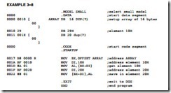
A short program, listed in Example 3–8, moves array element 10H into array element 20H. Notice that the array element number, loaded into the DI register, addresses the array element. Also notice how the contents of the ARRAY have been initialized so that element 10H contains 29H.
Addressing Modes-0064

Register Relative Addressing

Register relative addressing is similar to base-plus-index addressing and displacement addressing. In register relative addressing, the data in a segment of memory are addressed by

Addressing Modes-0065

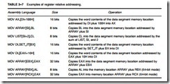
adding the displacement to the contents of a base or an index register (BP, BX, DI, or SI). Figure 3–10 shows the operation of the MOV AX,[BX + 1000H] instruction. In this example, BX = 0100H and DS = 0200H, so the address generated is the sum of DS * 0H, BX, and the displacement of 1000H, which addresses location 03100H. Remember that BX, DI, or SI addresses the data segment and BP addresses the stack segment. In the 80386 and above, the displacement can be a 32-bit number and the register can be any 32-bit register except the ESP register. Remember that the size of a real mode segment is 64K bytes long. Table 3–7 lists a few instructions that use register relative addressing

The displacement is a number added to the register within the [ ], as in the MOV AL,[DI + 2] instruction, or it can be a displacement is subtracted from the register, as in MOV AL,[SI–l]. A displacement also can be an offset address appended to the front of the [ ], as in MOV AL,DATA[DI]. Both forms of displacements also can appear simultaneously, as in the MOV AL,DATA[DI + 3] instruction. Both forms of the displacement add to the base or base plus index register within the [ ] symbols. In the 8086–80286 microprocessors, the value of the dis- placement is limited to a 16-bit signed number with a value ranging between + 32,767 (7FFFH)
Addressing Modes-0066Addressing Modes-0067

and –32,768 (8000H); in the 80386 and above, a 32-bit displacement is allowed with a value ranging between + 2,147,483,647 (7FFFFFFFH) and – 2,147,483,648 (80000000H).

Addressing Array Data with Register Relative. It is possible to address array data with register relative addressing, such as one does with base-plus-index addressing. In Figure 3–11, register relative addressing is illustrated with the same example as for base-plus-index addressing. This shows how the displacement ARRAY adds to index register DI to generate a reference to an array element.

Example 3–9 shows how this new addressing mode can transfer the contents of array element 10H into array element 20H. Notice the similarity between this example and Example 3–8. The main difference is that, in Example 3–9, register BX is not used to address memory ARRAY; instead, ARRAY is used as a displacement to accomplish the same task.

Addressing Modes-0068Addressing Modes-0069

Base Relative-Plus-Index Addressing

The base relative-plus-index addressing mode is similar to base-plus-index addressing, but it adds a displacement, besides using a base register and an index register, to form the memory address. This type of addressing mode often addresses a two-dimensional array of memory data.

Addressing Data with Base Relative-Plus-Index. Base relative-plus-index addressing is the least-used addressing mode. Figure 3–12 shows how data are referenced if the instruction exe- cuted by the microprocessor is MOV AX,[BX + SI + 100H]. The displacement of 100H adds to BX and SI to form the offset address within the data segment. Registers BX = 0020H, SI = 0100H, and DS = 1000H, so the effective address for this instruction is 10130H—the sum of these registers plus a displacement of 100H. This addressing mode is too complex for frequent use in programming. Some typical instructions using base relative-plus-index addressing appear in Table 3–8. Note that with the 80386 and above, the effective address is generated by the sum of two 32-bit registers plus a 32-bit displacement.

Addressing Modes-0070Addressing Modes-0071

Addressing Arrays with Base Relative-Plus-Index. Suppose that a file of many records exists in memory and each record contains many elements. The displacement addresses the file, the base register addresses a record, and the index register addresses an element of a record. Figure 3–13 illustrates this very complex form of addressing.

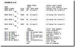
Example 3–10 provides a program that copies element 0 of record A into element 2 of record C by using the base relative-plus-index mode of addressing. This example FILE contains four records and each record contains 10 elements. Notice how the THIS BYTE statement is used to define the label FILE and RECA as the same memory location.
Addressing Modes-0072Addressing Modes-0073

Scaled-Index Addressing

Scaled-index addressing is the last type of data-addressing mode discussed. This data-addressing mode is unique to the 80386 through the Core2 microprocessors. Scaled-index addressing uses two 32-bit registers (a base register and an index register) to access the memory. The second register (index) is multiplied by a scaling factor. The scaling factor can be 1 × , 2 × , 4 × , or 8 × . A scaling factor of 1 × is implied and need not be included in the assembly language instruction (MOV AL,[EBX + ECX]). A scaling factor of 2 × is used to address word-sized memory arrays, a scaling factor of 4 × is used with doubleword-sized memory arrays, and a scaling factor of 8 × is used with quadword-sized memory arrays.

An example instruction is MOV AX,[EDI + 2*ECX]. This instruction uses a scaling factor of 2 × , which multiplies the contents of ECX by 2 before adding it to the EDI register to form the memory address. If ECX contains a 00000000H, word-sized memory element 0 is addressed; if ECX contains a 00000001H, word-sized memory element 1 is accessed, and so forth. This scales the index (ECX) by a factor of 2 for a word-sized memory array. Refer to Table 3–9 for some examples of scaled-index addressing. As you can imagine, there are an extremely large number of the scaled-index addressed register combinations. Scaling is also applied to instructions that use a single indirect register to access memory. The MOV EAX,[4*EDI] is a scaled-index instruction that uses one register to indirectly address memory. In the 64-bit mode, an instruction such as MOV RAX,[8*RDI] might appear in a program.

Example 3–11 shows a sequence of instructions that uses scaled-index addressing to access a word-sized array of data called LIST. Note that the offset address of LIST is loaded into register EBX with the MOV EBX,OFFSET LIST instruction. Once EBX addresses array LIST, the ele- ments (located in ECX) of 2, 4, and 7 of this word-wide array are added, using a scaling factor of 2 to access the elements. This program stores the 2 at element 2 into elements 4 and 7. Also notice the .386 directive to select the 80386 microprocessor. This directive must follow the .MODEL statement for the assembler to process 80386 instructions for DOS. If the 80486 is in use, the .486 directive appears after the .MODEL statement; if the Pentium is in use, then use .586; and if the Pentium Pro, Pentium II, Pentium III, Pentium 4, or Core2 is in use, then use the .686 directive. If the microprocessor selection directive appears before the .MODEL statement, the microprocessor executes instructions in the 32-bit protected mode, which must execute in Windows.

Addressing Modes-0074Addressing Modes-0075

RIP Relative Addressing

This form of addressing uses the 64-bit instruction pointer register in the 64-bit mode to address a linear location in the flat memory model. The inline assembler program available to Visual C ++ does not contain any way of using this addressing mode or any other 64-bit addressing mode. The Microsoft Visual C ++ does not at present support developing 64-bit assembly code. The instruction pointer is normally addressed using a * as in *+ 34, which is 34 bytes ahead in a program. When Microsoft finally places an inline assembler into Visual C ++ for the 64-bit mode, this most likely will be the way that RIP relative addressing will appear.

One source is Intel, which does produce a compiler with an inline assembler for 64-bit code (http://www.intel.com/cd/software/products/asmo-na/eng/compilers/cwin/279582.htm).

Data Structures

A data structure is used to specify how information is stored in a memory array and can be quite useful with applications that use arrays. It is best to think of a data structure as a template for data. The start of a structure is identified with the STRUC assembly language directive and the end with the ENDS statement. A typical data structure is defined and used three times in Example 3–12. Notice that the name of the structure appears with the STRUC and with ENDS statement. The example shows the data structure as it was typed without the assembled version.

Addressing Modes-0076

The data structure in Example 3–12 defines five fields of information. The first is 32 bytes long and holds a name; the second is 32 bytes long and holds a street address; the third is 16 bytes long for the city; the fourth is 2 bytes long for the state; the fifth is 5 bytes long for the ZIP code. Once the structure is defined (INFO), it can be filled, as illustrated, with names and addresses. Three example uses for INFO are illustrated. Note that literals are surrounded with apostrophes and the entire field is surrounded with < > symbols when the data structure is used to define data.

When data are addressed in a structure, use the structure name and the field name to select a field from the structure. For example, to address the STREET in NAME2, use the operand NAME2.STREET, where the name of the structure is first followed by a period and then by the name of the field. Likewise, use NAME3.CITY to refer to the city in structure NAME3.

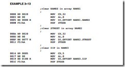
A short sequence of instructions appears in Example 3-13 that clears the name field in structure NAME1, the address field in structure NAME2, and the ZIP code field in structure NAME3. The function and operation of the instructions in this program are defined in later chapters in the text. You may wish to refer to this example once you learn these instructions.
Addressing Modes-0077


QUESTIONS AND PROBLEMS ON THE MICROPROCESSOR AND ITS ARCHITECTURE.

QUESTIONS AND PROBLEMS

1. What are program-visible registers?

2. The 80286 addresses registers that are 8 and bits wide.

3. The extended registers are addressable by which microprocessors?

4. The extended BX register is addressed as .

5. Which register holds a count for some instructions?

6. What is the purpose of the IP/EIP register?

7. The carry flag bit is not modified by which arithmetic operations?

8. Will an overflow occur if a signed FFH is added to a signed 01H?

9. A number that contains 3 one bits is said to have parity.

10. Which flag bit controls the INTR pin on the microprocessor?

11. Which microprocessors contain an FS segment register?

12. What is the purpose of a segment register in the real mode operation of the microprocessor?

13. In the real mode, show the starting and ending addresses of each segment located by the following segment register values:

(a) 1000H

(b) 1234H

(c) 2300H

(d) E000H

(e) AB00H

14. Find the memory address of the next instruction executed by the microprocessor, when oper- ated in the real mode, for the following CS:IP combinations:

(a) CS = 1000H and IP = 2000H

(b) CS = 2000H and IP = 1000H

(c) CS = 2300H and IP = 1A00H

(d) CS = 1A00H and IP = B000H

(e) CS = 3456H and IP = ABCDH

15. Real mode memory addresses allow access to memory below which memory address?

16. Which register or registers are used as an offset address for the string instruction destination in the microprocessor?

17. Which 32-bit register or registers are used to hold an offset address for data segment data in the Pentium 4 microprocessor?

18. The stack memory is addressed by a combination of the _________ segment plus offset.

19. If the base pointer (BP) addresses memory, the segment contains the data.

20. Determine the memory location addressed by the following real mode 80286 register combinations:

(a)DS = 1000H and DI = 2000H

(b) DS = 2000H and SI = 1002H

(c)SS = 2300H and BP = 3200H

(d) DS = A000H and BX = 1000H

(e)SS = 2900H and SP = 3A00H

21. Determine the memory location addressed by the following real mode Core2 register combinations:

(a)DS = 2000H and EAX = 00003000H

(b) DS = 1A00H and ECX = 00002000H

(c)DS = C000H and ESI = 0000A000H

(d) SS = 8000H and ESP = 00009000H

(e)DS = 1239H and EDX = 0000A900H

22. Protected mode memory addressing allows access to which area of the memory in the 80286 microprocessor?

23. Protected mode memory addressing allows access to which area of the memory in the Pentium 4 microprocessor?

24. What is the purpose of the segment register in protected mode memory addressing?

25. How many descriptors are accessible in the global descriptor table in the protected mode?

26. For an 80286 descriptor that contains a base address of A00000H and a limit of 1000H, what starting and ending locations are addressed by this descriptor?

27. For a Core2 descriptor that contains a base address of 01000000H, a limit of 0FFFFH, and G = 0, what starting and ending locations are addressed by this descriptor?

28. For a Core2 descriptor that contains a base address of 00280000H, a limit of 00010H, and G = 1, what starting and ending locations are addressed by this descriptor?

29. If the DS register contains 0020H in a protected mode system, which global descriptor table entry is accessed?

30. If DS = 0103H in a protected mode system, the requested privilege level is .

31. If DS = 0105H in a protected mode system, which entry, table, and requested privilege level are selected?

32. What is the maximum length of the global descriptor table in the Pentium 4 microprocessor?

33. Code a descriptor that describes a memory segment that begins at location 210000H and ends at location 21001FH. This memory segment is a code segment that can be read. The descriptor is for an 80286 microprocessor.

34. Code a descriptor that describes a memory segment that begins at location 03000000H and ends at location 05FFFFFFH. This memory segment is a data segment that grows upward in the memory system and can be written. The descriptor is for a Pentium 4 microprocessor.

35. Which register locates the global descriptor table?

36. How is the local descriptor table addressed in the memory system?

37. Describe what happens when a new number is loaded into a segment register when the microprocessor is operated in the protected mode.

38. What are the program-invisible registers?

39. What is the purpose of the GDTR?

40. How many bytes are found in a memory page?

41. What register is used to enable the paging mechanism in the 80386, 80486, Pentium, Pentium Pro, Pentium 4, and Core2 microprocessors?

42. How many 32-bit addresses are stored in the page directory?

43. Each entry in the page directory translates how much linear memory into physical memory?

44. If the microprocessor sends linear address 00200000H to the paging mechanism, which paging directory entry is accessed, and which page table entry is accessed?

45. What value is placed in the page table to redirect linear address 20000000H to physical address 30000000H?

46. What is the purpose of the TLB located within the Pentium class microprocessor?

47. Using the Internet, write a short report that details the TLB. Hint: You might want to go to the Intel Web site and search for information.

48. Locate articles about paging on the Internet and write a report detailing how paging is used in a variety of systems.

49. What is the flat mode memory system?

50. A flat mode memory system in the current version of the 64-bit Pentium 4 and Core2 allow these microprocessors to access bytes of memory.


SUMMARY OF THE MICROPROCESSOR AND ITS ARCHITECTURE.

SUMMARY

1. The programming model of the 8086 through 80286 contains 8- and 16-bit registers. The programming model of the 80386 and above contains 8-, 16-, and 32-bit extended registers as well as two additional 16-bit segment registers: FS and GS.

2. The 8-bit registers are AH, AL, BH, BL, CH, CL, DH, and DL. The 16-bit registers are AX, BX, CX, DX, SP, BP, DI, and SI. The segment registers are CS, DS, ES, SS, FS, and GS. The 32-bit extended registers are EAX, EBX, ECX, EDX, ESP, EBP, EDI, and ESI. The 64-bit registers in a Pentium 4 with 64-bit extensions are RAX, RBX, RCX, RDX, RSP, RBP, RDI, RSI, and R8 through R15. In addition, the microprocessor contains an instruction pointer (IP/EIP/RIP) and flag register (FLAGS, EFLAGS, or RFLAGS).

3. All real mode memory addresses are a combination of a segment address plus an offset address. The starting location of a segment is defined by the 16-bit number in the segment register that is appended with a hexadecimal zero at its rightmost end. The offset address is a 16-bit number added to the 20-bit segment address to form the real mode memory address.

4. All instructions (code) are accessed by the combination of CS (segment address) plus IP or EIP (offset address).

5. Data are normally referenced through a combination of the DS (data segment) and either an offset address or the contents of a register that contains the offset address. The 8086–Core2 use BX, DI, and SI as default offset registers for data if 16-bit registers are selected. The 80386 and above can use the 32-bit registers EAX, EBX, ECX, EDX, EDI, and ESI as default offset registers for data.

6. Protected mode operation allows memory above the first 1M byte to be accessed by the 80286 through the Core2 microprocessors. This extended memory system (XMS) is accessed via a segment address plus an offset address, just as in the real mode. The differ- ence is that the segment address is not held in the segment register. In the protected mode, the segment starting address is stored in a descriptor that is selected by the segment register.

7. A protected mode descriptor contains a base address, limit, and access rights byte. The base address locates the starting address of the memory segment; the limit defines the last location of the segment. The access rights byte defines how the memory segment is accessed via a program. The 80286 microprocessor allows a memory segment to start at any of its 16M bytes of memory using a 24-bit base address. The 80386 and above allow a memory segment to begin at any of its 4G bytes of memory using a 32-bit base address. The limit is a 16-bit number in the 80286 and a 20-bit number in the 80386 and above. This allows an 80286 memory segment limit of 64K bytes, and an 80386 and above memory segment limit of either 1M bytes (G = 0) or 4G bytes (G = 1). The L bit selects 64-bit address operation in the code descriptor.

8. The segment register contains three fields of information in the protected mode. The left- most 13 bits of the segment register address one of 8192 descriptors from a descriptor table. The TI bit accesses either the global descriptor table (TI = 0) or the local descriptor table (TI = 1). The rightmost 2 bits of the segment register select the requested priority level for the memory segment access.

9. The program-invisible registers are used by the 80286 and above to access the descriptor tables. Each segment register contains a cache portion that is used in protected mode to hold the base address, limit, and access rights acquired from a descriptor. The cache allows the microprocessor to access the memory segment without again referring to the descriptor table until the segment register’s contents are changed.

10. A memory page is 4K bytes in length. The linear address, as generated by a program, can be mapped to any physical address through the paging mechanism found within the 80386 through the Pentium 4 microprocessor.

11. Memory paging is accomplished through control registers CR0 and CR3. The PG bit of CR0 enables paging, and the contents of CR3 addresses the page directory. The page directory contains up to 1024 page table addresses that are used to access paging tables. The page table contains 1024 entries that locate the physical address of a 4K-byte memory page.

12. The TLB (translation look-aside buffer) caches the 32 most recent page table translations.

This precludes page table translation if the translation resides in the TLB, speeding the exe- cution of the software.

13. The flat mode memory contains 1T byte of memory using a 40-bit address. In the future, Intel plans to increase the address width to 52 bits to access 4P bytes of memory. The flat mode is only available in the Pentium 4 and Core2 that have their 64-bit extensions enabled.


THE MICROPROCESSOR AND ITS ARCHITECTURE:FLAT MODE MEMORY.

FLAT MODE MEMORY

The memory system in a Pentium-based computer (Pentium 4 or Core2) that uses the 64-bit extensions uses a flat mode memory system. A flat mode memory system is one in which there is no segmentation. The address of the first byte in the memory is at 00 0000 0000H and the last location is at FF FFFF FFFFH (address is 40-bits). The flat model does not use a segment register to address a location in the memory. The CS segment register is used to select a descriptor from the descriptor table that defines the access rights of only a code segment. The segment register still selects the privilege level of the software. The flat model does not select the memory address of a segment using the base and limit in the descriptor (see Figure 2–6). In 64-bit mode the actual address is not modified by the descriptor as in 32-bit protected mode. The offset address is the actual physical address in 64-bit mode. Refer to Figure 2–15 for the flat mode memory model.

This form of addressing is much easier to understand, but offers little protection to the system, through the hardware, as did the protected mode system discussed in Section 2.3. The real mode system is not available if the processor operates in the 64-bit mode. Protection and paging are allowed in the 64-bit mode. The CS register is still used in the protected mode operation in the 64-bit mode.

In the 64-bit mode if set to IA32 compatibility (when the L bit – 0 is in the descriptor), an address is 64-bits, but since only 40 bits of the address are brought out to the address pins, any address above 40 bits is truncated. Instructions that use a displacement address can only use a 32- bit displacement, which allows a range of ; 2G from the current instruction. This addressing mode is called RIP relative addressing, and is explained in Chapter 3. The move immediate instruction allows a full 64-bit address and access to any flat mode memory location. Other instructions do not allow access to a location above 4G because the offset address is still 32-bits.

If the Pentium is operated in the full 64-bit mode (where the L = 1 in the descriptor), the address may be 64-bits or 32-bits. This is shown in examples in the next chapter with addressing modes and in more detail in Chapter 4. Most programs today are operated in the IA32 compatible mode so current versions of Windows software operates properly, but this will change in a

The Microprocessor and Its Architecture-0042

few years as memory becomes larger and most people have 64-bit computers. This is another example of how the industry makes the software obsolete as the hardware changes.


THE MICROPROCESSOR AND ITS ARCHITECTURE:MEMORY PAGING.

MEMORY PAGING

The memory paging mechanism located within the 80386 and above allows any physical memory location to be assigned to any linear address. The linear address is defined as the address generated by a program. The physical address is the actual memory location accessed by a program. With the memory paging unit, the linear address is invisibly translated to any physical address, which allows an application written to function at a specific address to be relocated through the paging mechanism. It also allows memory to be placed into areas where no memory exists. An example is the upper memory blocks provided by EMM386.EXE in a DOS system.

The EMM386.EXE program reassigns extended memory, in 4K blocks, to the system memory between the video BIOS and the system BIOS ROMS for upper memory blocks. Without the paging mechanism, the use of this area of memory is impossible.

In Windows, each application is allowed a 2G linear address space from location 00000000H–7FFFFFFFH even though there may not be enough memory or memory available at these addresses. Through paging to the hard disk drive and paging to the memory through the memory paging unit, any Windows application can be executed.

Paging Registers

The paging unit is controlled by the contents of the microprocessor’s control registers. See Figure 2–11 for the contents of control registers CR0 through CR4. Note that these registers are available to the 80386 through the Core2 microprocessors. Beginning with the Pentium, an additional control register labeled CR4 controls extensions to the basic architecture provided in the Pentium or newer microprocessor. One of these features is a 2M- or a 4M-byte page that is enabled by controlling CR4.

The registers important to the paging unit are CR0 and CR3. The leftmost bit (PG) position of CR0 selects paging when placed at a logic 1 level. If the PG bit is cleared (0), the linear address generated by the program becomes the physical address used to access memory. If the PG bit is set (1), the linear address is converted to a physical address through the paging mechanism. The paging mechanism functions in both the real and protected modes.

CR3 contains the page directory base or root address, and the PCD and PWT bits. The PCD and PWT bits control the operation of the PCD and PWT pins on the microprocessor. If PCD is set (1), the PCD pin becomes a logic one during bus cycles that are not paged. This allows the external hardware to control the level 2 cache memory. (Note that the level 2 cache memory is an internal [on modern versions of the Pentium] high-speed memory that functions as a buffer between the microprocessor and the main DRAM memory system.) The PWT bit also appears on the PWT pin during bus cycles that are not paged to control the write-through cache in the system. The page directory base address locates the directory for the page translation unit. Note that this address locates the page directory at any 4K boundary in the memory system because it is appended internally with 000H. The page directory contains 1024 directory entries of 4 bytes each. Each page directory entry addresses a page table that contains 1024 entries.

The Microprocessor and Its Architecture-0039

The Microprocessor and Its Architecture-0040

The linear address, as it is generated by the software, is broken into three sections that are used to access the page directory entry, page table entry, and memory page offset address. Figure 2–12 shows the linear address and its makeup for paging. Notice how the leftmost 10 bits address an entry in the page directory. For linear address 00000000H–003FFFFFH, the first page directory is accessed. Each page directory entry represents or repages a 4M section of the memory system. The contents of the page directory select a page table that is indexed by the next 10 bits of the linear address (bit positions 12–21). This means that address 00000000H–00000FFFH selects page directory entry of 0 and page table entry of 0. Notice this is a 4K-byte address range. The off- set part of the linear address (bit positions 0–11) next selects a byte in the 4K-byte memory page. In Figure 2–12, if the page table entry 0 contains address 00100000H, then the physical address is 00100000H-00100FFFH for linear address 00000000H–00000FFFH. This means that when the program accesses a location between 00000000H and 00000FFFH, the microprocessor physically addresses location 00100000H–00100FFFH.

Because the act of repaging a 4K-byte section of memory requires access to the page directory and a page table, which are both located in memory, Intel has incorporated a special type of cache called the TLB (translation look-aside buffer). In the 80486 microprocessor, the cache holds the 32 most recent page translation addresses. This means that the last 32 page table trans- lations are stored in the TLB, so if the same area of memory is accessed, the address is already present in the TLB, and access to the page directory and page tables is not required. This speeds program execution. If a translation is not in the TLB, the page directory and page table must be accessed, which requires additional execution time. The Pentium–Pentium 4 microprocessors contain separate TLBs for each of their instruction and data caches.

The Page Directory and Page Table

Figure 2–13 shows the page directory, a few page tables, and some memory pages. There is only one page directory in the system. The page directory contains 1024 doubleword addresses that locate up to 1024 page tables. The page directory and each page table are 4K bytes in length. If

The Microprocessor and Its Architecture-0041

the entire 4G byte of memory is paged, the system must allocate 4K bytes of memory for the page directory, and 4K times 1024 or 4M bytes for the 1024 page tables. This represents a con- siderable investment in memory resources.

The DOS system and EMM386.EXE use page tables to redefine the area of memory between locations C8000H–EFFFFH as upper memory blocks. This is done by repaging extended memory to backfill this part of the conventional memory system to allow DOS access to additional memory. Suppose that the EMM386.EXE program allows access to 16M bytes of extended and conventional memory through paging and locations C8000H–EFFFFH must be repaged to locations 110000–138000H, with all other areas of memory paged to their normal locations. Such a scheme is depicted in Figure 2–14.

Here, the page directory contains four entries. Recall that each entry in the page directory corresponds to 4M bytes of physical memory. The system also contains four page tables with 1024 entries each. Recall that each entry in the page table repages 4K bytes of physical memory. This scheme requires a total of 16K of memory for the four page tables and 16 bytes of memory for the page directory.

As with DOS, the Windows program also repages the memory system. At present, Windows version 3.11 supports paging for only 16M bytes of memory because of the amount of memory required to store the page tables. Newer versions of Windows repage the entire memory system. On the Pentium–Core2 microprocessors, pages can be 4K, 2M, or 4M bytes in length. In the 2M and 4M variations, there is only a page directory and a memory page, but no page table.


THE MICROPROCESSOR AND ITS ARCHITECTURE:INTRODUCTION TO PROTECTED MODE MEMORY ADDRESSING.

INTRODUCTION TO PROTECTED MODE MEMORY ADDRESSING

Protected mode memory addressing (80286 and above) allows access to data and programs located above the first 1M byte of memory, as well as within the first 1M byte of memory. Protected mode is where Windows operates. Addressing this extended section of the memory system requires a change to the segment plus an offset addressing scheme used with real mode memory addressing. When data and programs are addressed in extended memory, the offset address is still used to access information located within the memory segment. One difference is that the segment address, as discussed with real mode memory addressing, is no longer present in the protected mode. In place of the segment address, the segment register contains a selector that selects a descriptor from a descriptor table. The descriptor describes the memory segment’s location, length, and access rights. Because the segment register and offset address still access memory, protected mode instructions are identical to real mode instructions. In fact, most programs written to function in the real mode will function without change in the protected mode. The difference between modes is in the way that the segment register is interpreted by the microprocessor to access the memory segment. Another difference, in the 80386 and above, is that the offset address can be a 32-bit number instead of a 16-bit number in the protected mode. A 32-bit offset address allows the microprocessor to access data within a segment that can be up to 4G bytes in length. Programs that are written for the 32-bit protected mode execute in the 64-bit mode of the Pentium 4.

Selectors and Descriptors

The selector, located in the segment register, selects one of 8192 descriptors from one of two tables of descriptors. The descriptor describes the location, length, and access rights of the seg- ment of memory. Indirectly, the segment register still selects a memory segment, but not directly as in the real mode. For example, in the real mode, if CS = 0008H, the code segment begins at location 00080H. In the protected mode, this segment number can address any memory location in the entire system for the code segment, as explained shortly.

There are two descriptor tables used with the segment registers: one contains global descriptors and the other contains local descriptors. The global descriptors contain segment definitions that apply to all programs, whereas the local descriptors are usually unique to an application. You might call a global descriptor a system descriptor and call a local descriptor an application descriptor. Each descriptor table contains 8192 descriptors, so a total of 16,384 total descriptors are available to an application at any time. Because the descriptor describes a memory segment, this allows up to 16,384 memory segments to be described for each application. Since a memory segment can be up to 4G bytes in length, this means that an application could have access to 4G * 16,384 bytes of memory or 64T bytes.

Figure 2–6 shows the format of a descriptor for the 80286 through the Core2. Note that each descriptor is 8 bytes in length, so the global and local descriptor tables are each a maximum of 64K bytes in length. Descriptors for the 80286 and the 80386–Core2 differ slightly, but the 80286 descriptor is upward-compatible.

The base address portion of the descriptor indicates the starting location of the memory segment. For the 80286 microprocessor, the base address is a 24-bit address, so segments begin at any location in its 16M bytes of memory. Note that the paragraph boundary limitation is

The Microprocessor and Its Architecture-0034

removed in these microprocessors when operated in the protected mode so segments may begin at any address. The 80386 and above use a 32-bit base address that allows segments to begin at any location in its 4G bytes of memory. Notice how the 80286 descriptor’s base address is upward-compatible to the 80386 through the Pentium 4 descriptor because its most-significant 16 bits are 0000H. Refer to Chapters 18 and 19 for additional detail on the 64G memory space provided by the Pentium Pro through the Core2.

The segment limit contains the last offset address found in a segment. For example, if a segment begins at memory location F00000H and ends at location F000FFH, the base address is F00000H and the limit is FFH. For the 80286 microprocessor, the base address is F00000H and the limit is 00FFH. For the 80386 and above, the base address is 00F00000H and the limit is 000FFH. Notice that the 80286 has a 16-bit limit and the 80386 through the Pentium 4 have a 20-bit limit. An 80286 can access memory segments that are between 1 and 64K bytes in length. The 80386 and above access memory segments that are between 1 and 1M byte, or 4K and 4G bytes in length.

There is another feature found in the 80386 through the Pentium 4 descriptor that is not found in the 80286 descriptor: the G bit, or granularity bit. If G = 0, the limit specifies a segment limit of 00000H to FFFFFH. If G = 1, the value of the limit is multiplied by 4K bytes (appended with FFFH). The limit is then 00000FFFFH to FFFFFFFFH, if G = 1. This allows a segment length of 4K to 4G bytes in steps of 4K bytes. The reason that the segment length is 64K bytes in the 80286 is that the offset address is always 16 bits because of its 16-bit internal architecture. The 80386 and above use a 32-bit architecture that allows an offset address, in the protected mode operation, of the 32 bits. This 32-bit offset address allows segment lengths of 4G bytes and the 16-bit offset address allows segment lengths of 64K bytes. Operating systems operate in a 16- or 32-bit environment. For example, DOS uses a 16-bit environment, while most Windows applications use a 32-bit environment called WIN32.

In the 64-bit descriptor, the L bit (probably means large, but Intel calls it the 64-bit) selects 64-bit addresses in a Pentium 4 or Core2 with 64-bit extensions when L = 1 and 32-bit compatibility mode when L = 0. In 64-bit protected operation, the code segment register is still used to select a section of code from the memory. Notice that the 64-bit descriptor has no limit or base address. It only contains an access rights byte and the control bits. In the 64-bit mode, there is no segment or limit in the descriptor and the base address of the segment, although not placed in the descriptor, is 00 0000 0000H. This means that all code segments start at address zero for 64-bit operation. There are no limit checks for a 64-bit code segment.

image

The AV bit, in the 80386 and above descriptor, is used by some operating systems to indicate that the segment is available (AV = 1) or not available (AV = 0). The D bit indicates how the 80386 through the Core2 instructions access register and memory data in the protected or real mode. If D = 0, the instructions are 16-bit instructions, compatible with the 8086–80286 microprocessors. This means that the instructions use 16-bit offset addresses and 16-bit register by default. This mode is often called the 16-bit instruction mode or DOS mode. If D = 1, the instructions are 32-bit instructions. By default, the 32-bit instruction mode assumes that all offset addresses and all registers are 32 bits. Note that the default for register size and offset address is overridden in both the 16- and 32-bit instruction modes. Both the MSDOS and PCDOS operating systems require that the instructions are always used in the 16-bit instruction mode. Windows 3.1, and any application that was writ- ten for it, also requires that the 16-bit instruction mode is selected. Note that the instruction mode is accessible only in a protected mode system such as Windows Vista. More detail on these modes and their application to the instruction set appears in Chapters 3 and 4.

The access rights byte (see Figure 2–7) controls access to the protected mode segment. This byte describes how the segment functions in the system. The access rights byte allows complete control over the segment. If the segment is a data segment, the direction of growth is specified. If the segment grows beyond its limit, the microprocessor’s operating system program is interrupted, indicating a general protection fault. You can even specify whether a data segment can be written or is write-protected. The code segment is also controlled in a similar fashion and can have reading inhibited to protect software. Again, note that in 64-bit mode there is only a code segment and no other segment descriptor types. A 64-bit flat model program contains its data and stacks in the code segment.

Descriptors are chosen from the descriptor table by the segment register. Figure 2–8 shows how the segment register functions in the protected mode system. The segment register contains a 13-bit selector field, a table selector bit, and a requested privilege level field. The 13-bit selector chooses one of the 8192 descriptors from the descriptor table. The TI bit selects either the global descriptor table (TI = 0) or the local descriptor table (TI = 1). The requested privilege level (RPL) requests the access privilege level of a memory segment. The highest privilege level is 00 and the lowest is 11. If the requested privilege level matches or is higher in priority than the privilege level set by the access rights byte, access is granted. For example, if the

The Microprocessor and Its Architecture-0036

requested privilege level is 10 and the access rights byte sets the segment privilege level at 11, access is granted because 10 is higher in priority than privilege level 11. Privilege levels are used in multiuser environments. Windows uses privilege level 00 (ring 0) for the kernel and driver programs and level 11 (ring 3) for applications. Windows does not use levels 01 or 10. If privi- lege levels are violated, the system normally indicates an application or privilege level violation.

Figure 2–9 shows how the segment register, containing a selector, chooses a descriptor from the global descriptor table. The entry in the global descriptor table selects a segment in the memory sys- tem. In this illustration, DS contains 0008H, which accesses the descriptor number 1 from the global descriptor table using a requested privilege level of 00. Descriptor number 1 contains a descriptor that defines the base address as 00100000H with a segment limit of 000FFH. This means that a value of 0008H loaded into DS causes the microprocessor to use memory locations 00100000H–001000FFH for the data segment with this example descriptor table. Note that descriptor zero is called the null descriptor, must contain all zeros, and may not be used for accessing memory.

The Microprocessor and Its Architecture-0037The Microprocessor and Its Architecture-0038

Program-Invisible Registers

The global and local descriptor tables are found in the memory system. In order to access and specify the address of these tables, the 80286–Core2 contain program-invisible registers. The program-invisible registers are not directly addressed by software so they are given this name (although some of these registers are accessed by the system software). Figure 2–10 illustrates the program-invisible registers as they appear in the 80286 through the Core2. These registers control the microprocessor when operated in protected mode.

Each of the segment registers contains a program-invisible portion used in the protected mode. The program-invisible portion of these registers is often called cache memory because cache is any memory that stores information. This cache is not to be confused with the level 1 or level 2 caches found with the microprocessor. The program-invisible portion of the segment register is loaded with the base address, limit, and access rights each time the number segment register is changed. When a new segment number is placed in a segment register, the micro- processor accesses a descriptor table and loads the descriptor into the program-invisible portion of the segment register. It is held there and used to access the memory segment until the segment number is again changed. This allows the microprocessor to repeatedly access a memory segment without referring to the descriptor table (hence the term cache).

The GDTR (global descriptor table register) and IDTR (interrupt descriptor table register) contain the base address of the descriptor table and its limit. The limit of each descriptor

The Microprocessor and Its Architecture-0039

table is 16 bits because the maximum table length is 64K bytes. When the protected mode operation is desired, the address of the global descriptor table and its limit are loaded into the GDTR. Before using the protected mode, the interrupt descriptor table and the IDTR must also be initialized. More detail is provided on protected mode operation later in the text. At this point, programming and additional description of these registers are impossible.

The location of the local descriptor table is selected from the global descriptor table. One of the global descriptors is set up to address the local descriptor table. To access the local descriptor table, the LDTR (local descriptor table register) is loaded with a selector, just as a segment register is loaded with a selector. This selector accesses the global descriptor table and loads the address, limit, and access rights of the local descriptor table into the cache portion of the LDTR.

The TR (task register) holds a selector, which accesses a descriptor that defines a task. A task is most often a procedure or application program. The descriptor for the procedure or application program is stored in the global descriptor table, so access can be controlled through the privilege levels. The task register allows a context or task switch in about 17 μs. Task switching allows the microprocessor to switch between tasks in a fairly short amount of time. The task switch allows multitasking systems to switch from one task to another in a simple and orderly fashion.


THE MICROPROCESSOR AND ITS ARCHITECTURE:REAL MODE MEMORY ADDRESSING.

REAL MODE MEMORY ADDRESSING

The 80286 and above operate in either the real or protected mode. Only the 8086 and 8088 operate exclusively in the real mode. In the 64-bit operation mode of the Pentium 4 and Core2, there is no real mode operation. This section of the text details the operation of the microprocessor in the real mode. Real mode operation allows the microprocessor to address only the first 1M byte of memory space—even if it is the Pentium 4 or Core2 microprocessor. Note that the first 1M byte of memory is called the real memory, conventional memory, or DOS memory system. The DOS operating sys- tem requires that the microprocessor operates in the real mode. Windows does not use the real mode. Real mode operation allows application software written for the 8086/8088, which only contains 1M byte of memory, to function in the 80286 and above without changing the software. The upward compatibility of software is partially responsible for the continuing success of the Intel family of microprocessors. In all cases, each of these microprocessors begins operation in the real mode by default whenever power is applied or the microprocessor is reset. Note that if the Pentium 4 or Core2 operate in the 64-bit mode, it cannot execute real mode applications; hence, DOS applications will not execute in the 64-bit mode unless a program that emulates DOS is written for the 64-bit mode.

Segments and Offsets

A combination of a segment address and an offset address accesses a memory location in the real mode. All real mode memory addresses must consist of a segment address plus an offset address. The segment address, located within one of the segment registers, defines the beginning address of any 64K-byte memory segment. The offset address selects any location within the 64K byte memory segment. Segments in the real mode always have a length of 64K bytes. Figure 2–3 shows how the segment plus offset addressing scheme selects a memory location. This illustration shows a memory segment that begins at location 10000H and ends at location IFFFFH—64K bytes in length. It also shows how an offset address, sometimes called a displacement, of F000H selects location 1F000H in the memory system. Note that the offset or displacement is the distance above the start of the segment, as shown in Figure 2–3.

The segment register in Figure 2–3 contains 1000H, yet it addresses a starting segment at location 10000H. In the real mode, each segment register is internally appended with a 0H on its rightmost end. This forms a 20-bit memory address, allowing it to access the start of a segment. The microprocessor must generate a 20-bit memory address to access a location within the first 1M of memory. For example, when a segment register contains 1200H, it addresses a 64K-byte memory segment beginning at location 12000H. Likewise, if a segment register contains 1201H, it addresses a memory segment beginning at location 12010H. Because of the internally appended 0H, real mode segments can begin only at a l6-byte boundary in the memory system. This l6-byte boundary is often called a paragraph.

Because a real mode segment of memory is 64K in length, once the beginning address is known, the ending address is found by adding FFFFH. For example, if a segment register con- tains 3000H, the first address of the segment is 30000H, and the last address is 30000H + FFFFH or 3FFFFH. Table 2–2 shows several examples of segment register contents and the starting and ending addresses of the memory segments selected by each segment address.

The offset address, which is a part of the address, is added to the start of the segment to address a memory location within the memory segment. For example, if the segment address is FIGURE 2–3 The real mode memory-addressing scheme, using a segment address plus an offset.

The Microprocessor and Its Architecture-0029

1000H and the offset address is 2000H, the microprocessor addresses memory location 12000H. The offset address is always added to the starting address of the segment to locate the data. The segment and offset address is sometimes written as 1000:2000 for a segment address of 1000H with an offset of 2000H.

In the 80286 (with special external circuitry) and the 80386 through the Pentium 4, an extra 64K minus 16 bytes of memory is addressable when the segment address is FFFFH and the HIMEM.SYS driver for DOS is installed in the system. This area of memory (0FFFF0H– 10FFEFH) is referred to as high memory. When an address is generated using a segment address of FFFFH, the A20 address pin is enabled (if supported in older systems) when an offset is added. For example, if the segment address is FFFFH and the offset address is 4000H, the machine addresses memory location FFFF0H + 4000H or 103FF0H. Notice that the A20 address line is the one in address 103FF0H. If A20 is not supported, the address is generated as 03FF0H because A20 remains a logic zero.

Some addressing modes combine more than one register and an offset value to form an offset address. When this occurs, the sum of these values may exceed FFFFH. For example, the address accessed in a segment whose segment address is 4000H and whose offset address is specified as the sum of F000H plus 3000H will access memory location 42000H instead of location 52000H. When the F000H and 3000H are added, they form a l6-bit (modulo 16) sum of 2000H used as the offset address; not 12000H, the true sum. Note that the carry of 1 (F000H + 3000H = 12000H) is dropped for this addition to form the offset address of 2000H. The address is generated as 4000:2000 or 42000H.

The Microprocessor and Its Architecture-0030

Default Segment and Offset Registers

The microprocessor has a set of rules that apply to segments whenever memory is addressed. These rules, which apply in the real and protected mode, define the segment register and off- set register combination. For example, the code segment register is always used with the instruction pointer to address the next instruction in a program. This combination is CS:IP or CS:EIP, depending upon the microprocessor’s mode of operation. The code segment register defines the start of the code segment and the instruction pointer locates the next instruction within the code segment. This combination (CS:IP or CS:EIP) locates the next instruction executed by the microprocessor. For example, if CS = 1400H and IP>EIP = 1200H, the micro- processor fetches its next instruction from memory location 14000H + 1200H or 15200H.

Another of the default combinations is the stack. Stack data are referenced through the stack segment at the memory location addressed by either the stack pointer (SP/ESP) or the pointer (BP/EBP). These combinations are referred to as SS:SP (SS:ESP), or SS:BP (SS:EBP). For example, if SS = 2000H and BP = 3000H, the microprocessor addresses memory location 23000H for the stack segment memory location. Note that in real mode, only the rightmost 16 bits of the extended register address a location within the memory segment. In the 80386–Pentium 4, never place a number larger than FFFFH into an offset register if the microprocessor is operated in the real mode. This causes the system to halt and indicate an addressing error.

Other defaults are shown in Table 2–3 for addressing memory using any Intel micro- processor with 16-bit registers. Table 2–4 shows the defaults assumed in the 80386 and above using 32-bit registers. Note that the 80386 and above have a far greater selection of segment/ offset address combinations than do the 8086 through the 80286 microprocessors.

The 8086–80286 microprocessors allow four memory segments and the 80386–Core2 microprocessors allow six memory segments. Figure 2–4 shows a system that contains four memory segments. Note that a memory segment can touch or even overlap if 64K bytes of memory are not required for a segment. Think of segments as windows that can be moved over any area of memory to access data or code. Also note that a program can have more than four or six segments, but only access four or six segments at a time.

Suppose that an application program requires 1000H bytes of memory for its code, 190H bytes of memory for its data, and 200H bytes of memory for its stack. This application does not require an extra segment. When this program is placed in the memory system by DOS, it is loaded in the TPA at the first available area of memory above the drivers and other TPA program. This area is indicated by a free-pointer that is maintained by DOS. Program loading is handled automatically by the program loader located within DOS. Figure 2–5 shows how an application is stored in the memory system. The segments show an overlap because the amount of data in them does not require 64K bytes of memory. The side view of the segments clearly shows the overlap. It also shows how segments can be moved over any area of memory by changing the segment starting address. Fortunately, the DOS program loader calculates and assigns segment starting addresses.

Segment and Offset Addressing Scheme Allows Relocation

The segment and offset addressing scheme seems unduly complicated. It is complicated, but it also affords an advantage to the system. This complicated scheme of segment plus offset addressing

The Microprocessor and Its Architecture-0031The Microprocessor and Its Architecture-0032

The Microprocessor and Its Architecture-0033

the program. The segment and offset addressing scheme allows both programs and data to be relocated without changing a thing in a program or data. This is ideal for use in a general-purpose com- puter system in which not all machines contain the same memory areas. The personal computer memory structure is different from machine to machine, requiring relocatable software and data.

Because memory is addressed within a segment by an offset address, the memory segment can be moved to any place in the memory system without changing any of the offset addresses. This is accomplished by moving the entire program, as a block, to a new area and then changing only the contents of the segment registers. If an instruction is 4 bytes above the start of the segment, its offset address is 4. If the entire program is moved to a new area of memory, this offset address of 4 still points to 4 bytes above the start of the segment. Only the con- tents of the segment register must be changed to address the program in the new area of memory. Without this feature, a program would have to be extensively rewritten or altered before it is moved. This would require additional time or many versions of a program for the many different configurations of computer systems. This concept also applies to programs written to execute in the protected mode for Windows. In the Windows environment all programs are writ- ten assuming that the first 2G of memory are available for code and data. When the program is loaded, it is placed in the actual memory, which may be anywhere and a portion may be located on the disk in the form of a swap file.


THE MICROPROCESSOR AND ITS ARCHITECTURE:INTERNAL MICROPROCESSOR ARCHITECTURE.

The Microprocessor and Its Architecture

INTRODUCTION

This chapter presents the microprocessor as a programmable device by first looking at its internal programming model and then how its memory space is addressed. The architecture of the family of Intel microprocessors is presented simultaneously, as are the ways that the family members address the memory system.

The addressing modes for this powerful family of microprocessors are described for the real, protected, and flat modes of operation. Real mode memory (DOS memory) exists at locations 00000H–FFFFFH, the first 1M byte of the memory system, and is present on all versions of the microprocessor. Protected mode memory (Windows memory) exists at any location in the entire protected memory system, but is available only to the 80286–Core2, not to the earlier 8086 or 8088 microprocessors. Protected mode memory for the 80286 contains 16M bytes; for the 80386– Pentium, 4G bytes; and for the Pentium Pro through the Core2, either 4G or 64G bytes. With the 64-bit extensions enabled, the Pentium 4 and Core2 address 1T byte of memory in a flat memory model. Windows Vista or Windows 64 is needed to operate the Pentium 4 or Core2 in 64-bit mode using the flat mode memory to access the entire 1T byte of memory.

CHAPTER OBJECTIVES

Upon completion of this chapter, you will be able to:

1. Describe the function and purpose of each program-visible register in the 8086–Core2 microprocessors, including the 64-bit extensions.

2. Detail the flag register and the purpose of each flag bit.

3. Describe how memory is accessed using real mode memory-addressing techniques.

4. Describe how memory is accessed using protected mode memory-addressing techniques.

5. Describe how memory is accessed using the 64-bit flat memory model.

6. Describe the program-invisible registers found within the 80286 through Core2 microprocessors.

7. Detail the operation of the memory-paging mechanism.

INTERNAL MICROPROCESSOR ARCHITECTURE

Before a program is written or any instruction investigated, the internal configuration of the micro- processor must be known. This section of the chapter details the program-visible internal architecture of the 8086–Core2 microprocessors. Also detailed are the function and purpose of each of these internal registers. Note that in a multiple core microprocessor each core contains the same programming model. The only difference is that each core runs a separate task or thread simultaneously.

The Programming Model

The programming model of the 8086 through the Core2 is considered to be program visible because its registers are used during application programming and are specified by the instructions. Other registers, detailed later in this chapter, are considered to be program invisible because they are not addressable directly during applications programming, but may be used indirectly during system programming. Only the 80286 and above contain the program-invisible registers used to control and operate the protected memory system and other features of the microprocessor.

Figure 2–1 illustrates the programming model of the 8086 through the Core2 microprocessor including the 64-bit extensions. The earlier 8086, 8088, and 80286 contain 16-bit internal

The Microprocessor and Its Architecture-0022

architectures, a subset of the registers shown in Figure 2–1. The 80386 through the Core2 microprocessors contain full 32-bit internal architectures. The architectures of the earlier 8086 through the 80286 are fully upward-compatible to the 80386 through the Core2. The shaded areas in this illustration represent registers that are found in early versions of the 8086, 8088, or 80286 microprocessors and are provided on the 80386–Core2 microprocessors for compatibility to the early versions The programming model contains 8-, 16-, and 32-bit registers. The Pentium 4 and Core2 also contain 64-bit registers when operated in the 64-bit mode as illustrated in the programming model. The 8-bit registers are AH, AL, BH, BL, CH, CL, DH, and DL and are referred to when an instruction is formed using these two-letter designations. For example, an ADD AL,AH instruction adds the 8-bit contents of AH to AL. (Only AL changes due to this instruction.) The 16-bit registers are AX, BX, CX, DX, SP, BP, DI, SI, IP, FLAGS, CS, DS, ES, SS, FS, and GS.

Note that the first 4 16 registers contain a pair of 8-bit registers. An example is AX, which contains AH and AL. The 16-bit registers are referenced with the two-letter designations such as AX. For example, an ADD DX, CX instruction adds the 16-bit contents of CX to DX. (Only DX changes due to this instruction.) The extended 32-bit registers are EAX, EBX, ECX, EDX, ESP, EBP, EDI, ESI, EIP, and EFLAGS. These 32-bit extended registers, and 16-bit registers FS and GS, are available only in the 80386 and above. The 16-bit registers are referenced by the desig- nations FS or GS for the two new 16-bit registers, and by a three-letter designation for the 32-bit registers. For example, an ADD ECX, EBX instruction adds the 32-bit contents of EBX to ECX. (Only ECX changes due to this instruction.)

Some registers are general-purpose or multipurpose registers, while some have special purposes. The multipurpose registers include EAX, EBX, ECX, EDX, EBP, EDI, and ESI. These registers hold various data sizes (bytes, words, or doublewords) and are used for almost any purpose, as dictated by a program.

The 64-bit registers are designated as RAX, RBX, and so forth. In addition to the renaming of the registers for 64-bit widths, there are also additional 64-bit registers that are called R8 through R15. The 64-bit extensions have multiplied the available register space by more than 8 times in the Pentium 4 and the Core2 when compared to the original microprocessor architecture as indicated in the shaded area in Figure 2–1. An example 64-bit instruction is ADD RCX, RBX, instruction, which adds the 64-bit contents of RBX to RCX. (Only RCX changes due to this instruction.) One difference exists: these additional 64-bit registers (R8 through R15) are addressed as a byte, word, doubleword, or quadword, but only the rightmost 8 bits is a byte. R8 through R15 have no provision for directly addressing bits 8 through 15 as a byte. In the 64-bit mode, a legacy high byte register (AH, BH, CH, or DH) cannot be addressed in the same instruction with an R8 through R15 byte. Because legacy software does not access R8 through R15, this causes no problems with existing 32-bit programs, which function without modification.

Table 2–1 shows the overrides used to access portions of a 64-bit register. To access the low-order byte of the R8 register, use R8B (where B is the low-order byte). Likewise, to access the low-order word of a numbered register, such as R10, use R10W in the instruction. The letter D is used to access a doubleword. An example instruction that copies the low-order doubleword from R8 to R11 is MOV R11D, R8D. There is no special letter for the entire 64-bit register.

The Microprocessor and Its Architecture-0023

Multipurpose Registers

RAX RAX is referenced as a 64-bit register (RAX), a 32-bit register (accumulator) (EAX), a 16-bit register (AX), or as either of two 8-bit registers (AH and AL). Note that if an 8- or 16-bit register is addressed, only that portion of the 32-bit register changes without affecting the remaining bits. The accumulator is used for instructions such as multiplication, division, and some of the adjustment instructions. For these instructions, the accumulator has a special purpose, but is generally considered to be a multipurpose register. In the 80386 and above, the EAX register may also hold the offset address of a location in the memory system. In the 64-bit Pentium 4 and Core2, RAX holds a 64- bit offset address, which allows 1T (terra) byte of memory to be accessed through a 40-bit address bus. In the future, Intel plans to expand the address bus to 52 bits to address 4P (peta) bytes of memory.

RBX RBX is addressable as RBX, EBX, BX, BH, or BL. The BX register  (base index) sometimes holds the offset address of a location in the memory system in all versions of the microprocessor. In the 80386 and above, EBX also can address memory data. In the 64-bit Pentium 4 and Core2, RBX can also address memory data.

RCX RCX, which is addressable as RCX, ECX, CX, CH, or CL, is a (count) general-purpose register that also holds the count for various instructions. In the 80386 and above, the ECX register also can hold the offset address of memory data. In the 64-bit Pentium 4, RCX can also address memory data. Instructions that use a count are the repeated string instructions (REP/REPE/REPNE); and shift, rotate, and LOOP/LOOPD instructions. The shift and rotate instructions use CL as the count, the repeated string instructions use CX, and the LOOP/LOOPD instructions use either CX or ECX. If operated in the 64-bit mode, LOOP uses the 64-bit RCX register for the loop counter.

RDX RDX, which is addressable as RDX, EDX, DX, DH, or DL, is a (data) general-purpose register that holds a part of the result from a multiplication or part of the dividend before a division. In the 80386 and above, this register can also address memory data.

RBP RBP, which is addressable as RBP, EBP, or BP, points to a memory (base pointer) location in all versions of the microprocessor for memory data transfers.

RDI RDI, which is addressable as RDI, EDI, or DI, often addresses (destination index) string destination data for the string instructions.

RSI RSI is used as RSI, ESI, or SI. The source index register often (source index) addresses source string data for the string instructions. Like RDI, RSI also functions as a general-purpose register. As a 16-bit register, it is addressed as SI; as a 32-bit register, it is addressed as ESI; and as a 64-bit register, it is addressed as RSI.

R8 through R15 These registers are only found in the Pentium 4 and Core2 if 64-bit extensions are enabled. As mentioned, data in these registers are addressed as 64-, 32-, 16-, or 8-bit sizes and are of general purpose. Most applications will not use these registers until 64-bit processors are common. Please note that the 8-bit portion is the rightmost 8-bit only; bits 8 to 15 are not directly addressable as a byte.

The Microprocessor and Its Architecture-0025

A (auxiliary carry) The auxiliary carry holds the carry (half-carry) after addition or the borrow after subtraction between bit positions 3 and 4 of the result. This highly specialized flag bit is tested by the DAA and DAS instructions to adjust the value of AL after a BCD addition or subtraction. Otherwise, the A flag bit is not used by the microprocessor or any other instructions.

Z (zero) The zero flag shows that the result of an arithmetic or logic operation is zero. If Z = 1, the result is zero; if Z = 0, the result is not zero. This may be confusing, but that is how Intel decided to name this flag.

S (sign) The sign flag holds the arithmetic sign of the result after an arithmetic or logic instruction executes. If S = 1, the sign bit (leftmost bit of a number) is set or negative; if S = 0, the sign bit is cleared or positive.

T (trap) The trap flag enables trapping through an on-chip debugging feature. (A program is debugged to find an error or bug.) If the T flag is enabled (1), the microprocessor interrupts the flow of the program on conditions as indicated by the debug registers and control registers. If the T flag is a logic 0, the trapping (debugging) feature is disabled. The Visual C++ debugging tool uses the trap feature and debug registers to debug faulty software.

I (interrupt) The interrupt flag controls the operation of the INTR (interrupt request) input pin. If I = 1, the INTR pin is enabled; if I = 0, the INTR pin is disabled. The state of the I flag bit is controlled by the STI (set I flag) and CLI (clear I flag) instructions.

D (direction) The direction flag selects either the increment or decrement mode for the DI and/or SI registers during string instructions. If D = 1, the registers are automatically decremented; if D = 0, the registers are automatically incremented. The D flag is set with the STD (set direction) and cleared with the CLD (clear direction) instructions.

O (overflow) Overflows occur when signed numbers are added or subtracted. An overflow indicates that the result has exceeded the capacity of the machine. For example, if 7FH ( + 127) is added—using an 8-bit addition—to 01H ( + 1), the result is 80H (–128). This result represents an overflow condition indicated by the overflow flag for signed addition. For unsigned operations, the overflow flag is ignored.

IOPL IOPL is used in protected mode operation to select the privilege (I/O privilege level) level for I/O devices. If the current privilege level is higher or more trusted than the IOPL, I/O executes without hindrance. If the IOPL is lower than the current privilege level, an interrupt occurs, causing execution to suspend. Note that an IOPL of 00 is the highest or most trusted and an IOPL of 11 is the lowest or least trusted.

NT (nested task) The nested task flag indicates that the current task is nested within another task in protected mode operation. This flag is set when the task is nested by software.

RF (resume) The resume flag is used with debugging to control the resumption of execution after the next instruction.

VM (virtual mode) The VM flag bit selects virtual mode operation in a protected mode system. A virtual mode system allows multiple DOS memory partitions that are 1M byte in length to coexist in the memory system. Essentially, this allows the system program to execute multiple DOS programs. VM is used to simulate DOS in the modern Windows environment.

AC The alignment check flag bit activates if a word or doubleword is (alignment check) addressed on a non-word or non-doubleword boundary. Only the 80486SX microprocessor contains the alignment check bit that is primarily used by its companion numeric coprocessor, the 80487SX, for synchronization.

VIF The VIF is a copy of the interrupt flag bit available to the Pentium– (virtual interrupt) Pentium 4 microprocessors.

VIP (virtual VIP provides information about a virtual mode interrupt for the interrupt pending) Pentium–Pentium 4 microprocessors. This is used in multitasking environments to provide the operating system with virtual interrupt flags and interrupt pending information.

ID (identification) The ID flag indicates that the Pentium–Pentium 4 microprocessors support the CPUID instruction. The CPUID instruction provides the system with information about the Pentium microprocessor, such as its version number and manufacturer.

Segment Registers. Additional registers, called segment registers, generate memory addresses when combined with other registers in the microprocessor. There are either four or six segment registers in various versions of the microprocessor. A segment register func- tions differently in the real mode when compared to the protected mode operation of the micro- processor. Details on their function in real and protected mode are provided later in this chapter. In the 64-bit flat model, segment registers have little use in a program except for the code segment register. Following is a list of each segment register, along with its function in the system:

CS (code) The code segment is a section of memory that holds the code (programs and procedures) used by the microprocessor. The code segment register defines the starting address of the section of memory holding code. In real mode operation, it defines the start of a 64K- byte section of memory; in protected mode, it selects a descriptor that describes the starting address and length of a section of memory holding code. The code segment is limited to 64K bytes in the 8088–80286, and 4G bytes in the 80386 and above when these microprocessors operate in the protected mode. In the 64-bit mode, the code segment register is still used in the flat model, but its use differs from other programming modes as explained in Section 2-5.

DS (data) The data segment is a section of memory that contains most data used by a program. Data are accessed in the data segment by an offset address or the contents of other registers that hold the offset address. As with the code segment and other segments, the length is limited to 64K bytes in the 8086–80286, and 4G bytes in the 80386 and above.

ES (extra) The extra segment is an additional data segment that is used by some of the string instructions to hold destination data.

SS (stack) The stack segment defines the area of memory used for the stack.

The stack entry point is determined by the stack segment and stack pointer registers. The BP register also addresses data within the stack segment.

FS and GS The FS and GS segments are supplemental segment registers available in the 80386–Core2 microprocessors to allow two additional memory segments for access by programs. Windows uses these segments for internal operations, but no definition of their usage is available.