DIRECT MEMORY ACCESS AND DMA-CONTROLLED I/O:BASIC DMA OPERATION

DIRECT MEMORY ACCESS AND DMA-CONTROLLED I/O

INTRODUCTION

In previous chapters, we discussed basic and interrupt-processed I/O. Now we turn to the final form of I/O called direct memory access (DMA). The DMA I/O technique provides direct access to the memory while the microprocessor is temporarily disabled. This allows data to be transferred between memory and the I/O device at a rate that is limited only by the speed of the memory components in the system or the DMA controller. The DMA transfer speed can approach 33 to 150 M-byte transfer rates with today’s high-speed RAM memory components.

DMA transfers are used for many purposes, but more common are DRAM refresh, video displays for refreshing the screen, and disk memory system reads and writes. The DMA transfer is also used to do high-speed memory-to-memory transfers.

This chapter also explains the operation of disk memory systems and video systems that are often DMA-processed. Disk memory includes floppy, fixed, and optical disk storage. Video systems include digital and analog monitors.

CHAPTER OBJECTIVES

Upon completion of this chapter, you will be able to:

1. Describe a DMA transfer.

2. Explain the operation of the HOLD and HLDA direct memory access control signals.

3. Explain the function of the 8237 DMA controller when used for DMA transfers.

4. Program the 8237 to accomplish DMA transfers.

5. Describe the disk standards found in personal computer systems.

6. Describe the various video interface standards that are found in the personal computer.

BASIC DMA OPERATION

Two control signals are used to request and acknowledge a direct memory access (DMA) transfer in the microprocessor-based system. The HOLD pin is an input that is used to request a DMA action and the HLDA pin is an output that acknowledges the DMA action. Figure 13–1 shows the timing that is typically found on these two DMA control pins.

Direct Memory Access and DMA-Controlled I-O-0209

Whenever the HOLD input is placed at a logic 1 level, a DMA action (hold) is requested. The microprocessor responds, within a few clocks, by suspending the execution of the program and by placing its address, data, and control bus at their high-impedance states. The high-impedance state causes the microprocessor to appear as if it has been removed from its socket. This state allows external I/O devices or other microprocessors to gain access to the system buses so that memory can be accessed directly.

As the timing diagram indicates, HOLD is sampled in the middle of any clocking cycle. Thus, the hold can take effect any time during the operation of any instruction in the micro- processor’s instruction set. As soon as the microprocessor recognizes the hold, it stops executing software and enters hold cycles. Note that the HOLD input has a higher priority than the INTR or NMI interrupt inputs. Interrupts take effect at the end of an instruction, whereas a HOLD takes effect in the middle of an instruction. The only microprocessor pin that has a higher priority than a HOLD is the RESET pin. Note that the HOLD input may not be active during a RESET or the reset is not guaranteed.

The HLDA signal becomes active to indicate that the microprocessor has indeed placed its buses at their high-impedance state, as can be seen in the timing diagram. Note that there are a few clock cycles between the time that HOLD changes and until HLDA changes. The HLDA output is a signal to the external requesting device that the microprocessor has relinquished control of its memory and I/O space. You could call the HOLD input a DMA request input and the HLDA output a DMA grant signal.

Basic DMA Definitions

Direct memory accesses normally occur between an I/O device and memory without the use of the microprocessor. A DMA read transfers data from the memory to the I/O device. A DMA write transfers data from an I/O device to memory. In both operations, the memory and I/O are controlled simultaneously, which is why the system contains separate memory and I/O control signals. This special control bus structure of the microprocessor allows DMA transfers. A DMA read causes both the MRDC and IOWC signals to activate simultaneously, transferring data from the memory to the I/O device. A DMA write causes the MWTC and IORC signals to both acti- vate. These control bus signals are available to all microprocessors in the Intel family except the 8086/8088 system. The 8086/8088 require their generation with either a system controller or a circuit such as the one illustrated in Figure 13–2. The DMA controller provides the memory with its address and a signal from the controller (DACK) selects the I/O device during the DMA transfer.

The data transfer speed is determined by the speed of the memory device or a DMA controller that often controls DMA transfers. If the memory speed is 50 ns, DMA transfers occur at rates of up to 1/50 ns or 20 M bytes per second. If the DMA controller in a system functions at a maximum rate of 15 MHz and we still use 50 ns memory, the maximum transfer rate is 15 MHz because the DMA controller is slower than the memory. In many cases, the DMA controller slows the speed of the system when DMA transfers occur.

Direct Memory Access and DMA-Controlled I-O-0210

Because of the switch to serial data transfers in modern computer systems, DMA is becoming less important. The PCI Express bus, which is serial, transfers data at rates that exceed DMA transfers. Even the SATA (serial ATA) interface for disk drives uses serial transfers at the rate of 300 Mbps, which has replaced DMA transfers for hard disk drives. Serial transfers on main-boards (motherboards) between components that use serial techniques can approach 20 Gbps for the PCI Express connection.


QUESTIONS AND PROBLEMS ON INTERRUPTS.

QUESTIONS AND PROBLEMS

1. What is interrupted by an interrupt?

2. Define the term interrupt.

3. What is called by an interrupt?

4. Why do interrupts free up time for the microprocessor?

5. List the interrupt pins found on the microprocessor.

6. List the five interrupt instructions for the microprocessor.

7. What is an interrupt vector?

8. Where are the interrupt vectors located in the microprocessor’s memory?

9. How many different interrupt vectors are found in the interrupt vector table?

10. Which interrupt vectors are reserved by Intel?

11. Explain how a type 0 interrupt occurs.

12. Where is the interrupt descriptor table located for protected mode operation?

13. Each protected mode interrupt descriptor contains what information?

14. Describe the differences between a protected and real mode interrupt.

15. Describe the operation of the BOUND instruction.

16. Describe the operation of the INTO instruction.

17. What memory locations contain the vector for an INT 44H instruction?

18. Explain the operation of the IRET instruction.

19. Where is the IRETQ instruction used?

20. What is the purpose of interrupt vector type number 7?

21. List the events that occur when an interrupt becomes active.

22. Explain the purpose of the interrupt flag (IF).

23. Explain the purpose of the trap flag (TF).

24. How is IF cleared and set?

25. How is TF cleared and set?

26. The NMI interrupt input automatically vectors through which vector type number?

27. Does the INTA signal activate for the NMI pin?

28. The INTR input is -sensitive.

29. The NMI input is -sensitive.

30. When the INTA signal becomes a logic 0, it indicates that the microprocessor is waiting for an interrupt number to be placed on the data bus (D0–D7).

31. What is an FIFO?

32. Develop a circuit that places interrupt type number CCH on the data bus in response to the INTR input.

33. Develop a circuit that places interrupt type number 86H on the data bus in response to the INTR input.

34. Explain why pull-up resistors on D0–D7 cause the microprocessor to respond with interrupt vector type number FFH for the INTA pulse.

35. What is a daisy-chain?

36. Why must interrupting devices be polled in a daisy-chained interrupt system?

37. What is the 8259A?

38. How many 8259As are required to have 64 interrupt inputs?

39. What is the purpose of the IR0–IR7 pins on the 8259A?

40. When are the CAS2–CAS0 pins used on the 8259A?

41. Where is a slave INT pin connected on the master 8259A in a cascaded system?

42. What is an OCW?

43. What is an ICW?

44. Where is the vector type number stored in the 8259A?

45. How many ICWs are needed to program the 8259A when operated as a single master in a system?

46. What is the purpose of ICW1?

47. Where is the sensitivity of the IR pins programmed in the 8259A?

48. Explain priority rotation in the 8259A.

49. What is a nonspecific EOI?

50. At which interrupt vectors is the master 8259A found in the personal computer?

51. What is the purpose of IRR in the 8259A?

At which interrupt vectors is the slave 8259A found in the personal computer?


SUMMARY OF INTERRUPTS.

SUMMARY

1. An interrupt is a hardware- or software-initiated call that interrupts the currently executing program at any point and calls a procedure. The procedure is called by the interrupt handler or an interrupt service procedure.

2. Interrupts are useful when an I/O device needs to be serviced only occasionally at low data transfer rates.

3. The microprocessor has five instructions that apply to interrupts: BOUND, INT, INT 3, INTO, and IRET. The INT and INT 3 instructions call procedures with addresses stored in the interrupt vector whose type is indicated by the instruction. The BOUND instruction is a conditional interrupt that uses interrupt vector type number 5. The INTO instruction is a conditional interrupt that interrupts a program only if the overflow flag is set. Finally, the IRET, IRETD, or IRETQ instruction is used to return from interrupt service procedures.

4. The microprocessor has three pins that apply to its hardware interrupt structure: INTR, NMI, and INTA. The interrupt inputs are INTR and NMI, which are used to request interrupts, and INTA, an output used to acknowledge the INTR interrupt request.

5. Real mode interrupts are referenced through a vector table that occupies memory locations 0000H–03FFH. Each interrupt vector is four bytes long and contains the offset and segment addresses of the interrupt service procedure. In protected mode, the interrupts reference the interrupt descriptor table (IDT) that contains 256 interrupt descriptors. Each interrupt descriptor contains a segment selector and a 32-bit offset address.

6. Two flag bits are used with the interrupt structure of the microprocessor: trap (TF) and inter- rupt enable (IF). The IF flag bit enables the INTR interrupt input, and the TF flag bit causes interrupts to occur after the execution of each instruction, as long as TF is active.

7. The first 32 interrupt vector locations are reserved for Intel use, with many predefined in the microprocessor. The last 224 interrupt vectors are for the user’s use and can perform any function desired.

8. Whenever an interrupt is detected, the following events occur: (1) the flags are pushed onto the stack, (2) the IF and TF flag bits are both cleared, (3) the IP and CS registers are both pushed onto the stack, and (4) the interrupt vector is fetched from the interrupt vector table and the interrupt service subroutine is accessed through the vector address.

9. Tracing or single-stepping is accomplished by setting the TF flag bit. This causes an inter- rupt to occur after the execution of each instruction for debugging.

10. The non-maskable interrupt input (NMI) calls the procedure whose address is stored at inter- rupt vector type number 2. This input is positive edge-triggered.

11. The INTR pin is not internally decoded, as is the NMI pin. Instead, INTA is used to apply the interrupt vector type number to data bus connections D0–D7 during the INTA pulse.

12. Methods of applying the interrupt vector type number to the data bus during INTA vary widely. One method uses resisters to apply interrupt type number FFH to the data bus, while another uses a three-state buffer to apply any vector type number.

13. The 8259A programmable interrupt controller (PIC) adds at least eight interrupt inputs to the microprocessor. If more interrupts are needed, this device can be cascaded to provide up to 64 interrupt inputs.

14. Programming the 8259A is a two-step process. First, a series of initialization command words (ICWs) are sent to the 8259A, then a series of operation command words (OCWs) are sent.

15. The 8259A contains three status registers: IMR (interrupt mask register), ISR (in-service register), and IRR (interrupt request register).

16. A real-time clock is used to keep time in real time. In most cases, time is stored in either binary or BCD form in several memory locations.


INTERRUPTS:INTERRUPT EXAMPLES.

INTERRUPT EXAMPLES

This section of the text presents a real-time clock and an interrupt-processed keyboard as examples of interrupt applications. A real-time (RTC) clock keeps time in real time—that is, in hours and minutes. It is also used for precision time delays. The example illustrated here keeps time in Modem Control Register Modem Status Register

Interrupts-0199Interrupts-0200

hours, minutes, seconds, and l/60 second, using four memory locations to hold the BCD time of day. The interrupt-processed keyboard uses a periodic interrupt to scan through the keys of the keyboard.

Real-Time Clock

Figure 12–26 illustrates a simple circuit that uses the 60 Hz AC power line to generate a periodic interrupt request signal for the NMI interrupt input pin. Although we are using a signal from the AC power line, which varies slightly in frequency from time to time, it is accurate over a period of time as mandated by the Federal Trade Commission (FTC).

The circuit uses a signal from the 120 V AC power line that is conditioned by a Schmitt trigger inverter before it is applied to the NMI interrupt input. Note that you must make certain that the power line ground is connected to the system ground in this schematic. The power line neutral (white wire) connection is the wide flat pin on the power line. The narrow flat pin is the hot (black wire) side or 120 V AC side of the line.

Interrupts-0201

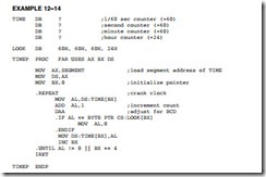
The software for the real-time clock contains an interrupt service procedure that is called 60 times per second and a procedure that updates the count located in four memory locations. Example 12–14 lists both procedures, along with the four bytes of memory used to hold the BCD time of day. The memory locations for the TIME are stored somewhere in the system memory at the segment address (SEGMENT) and at the offset address TIME, which is first loaded in the TIMEP procedure. The lookup table (LOOK) for the modulus or each counter is stored in the code segment with the procedure.

Interrupts-0202

Another way to handle time is to use a single counter to store the time in memory and then determine the actual time with software. For example, the time can be stored in one single 32-bit counter (there are 5,184,000 1/60 sec in a day). In a counter such as this, a count of 0 is 12:00:00:00 AM and a count of 5,183,999 is 11:59:59:59 PM. Example 12–15 shows the interrupt procedure for this type of RTC, which requires the least of amount of time to execute.

Interrupts-0203

Software to convert the count in the modulus 5,184,000 counter into hours, minutes, and seconds appears in Example 12–16. The procedure returns with the number of hours (0–23) in BL, number of minutes in BH, and number of seconds in AL. No attempt was made to retrieve the 1/60 second count.

Interrupts-0204

Suppose a time delay is needed. Time delays can be achieved using the RTC in Example 12–15 for any amount from 1/60 of a second to 24 hours. Example 12–17 shows a procedure that uses the RTC to perform time delays of the number of seconds passed to the procedure in the EAX register. This can be 1 second to an entire day’s worth of seconds. It has an accuracy to within 1/60 second, the resolution of the RTC.

Interrupts-0205

Interrupt-Processed Keyboard

The interrupt-processed keyboard scans through the keys on a keyboard through a periodic interrupt. Each time the interrupt occurs, the interrupt-service procedure tests for a key or debounces the key. Once a valid key is detected, the interrupt service procedure stores the key code into a keyboard queue for later reading by the system. The basis for this system is a periodic interrupt that can be caused by a timer, RTC, or other device in the system. Note that most systems already have a periodic interrupt for the real-time clock. In this example, we assume the interrupt calls the interrupt service procedure every 10 ms or, if the RTC is used with a 60 Hz clock, every 16.7 ms.

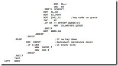
Figure 12–27 shows the keyboard interfaced to an 82C55. It does not show the timer or other circuitry required to call the interrupt once in every 10 ms or 16.7 ms. (Not shown in the software is programming of the 82C55.) The 82C55 must be programmed so that port A is an input port, port B is an output port, and the initialization software must store 00H at port B. This interfaces uses memory that is stored in the code segment for a queue and a few bytes that keep track of the keyboard scanning. Example 12–18 lists the interrupt service procedure for the keyboard.

Interrupts-0206Interrupts-0207

The keyboard-interrupt finds the key and stores the key code in the queue. The code stored in the queue is a raw code that does not indicate the key number. For example, the key code for the 1-key is 00H, the key code for the 4-key is 01H, and so on. There is no provision for a queue overflow in this software. It could be added, but in almost all cases it is difficult to out-type a 16-byte queue.

Example 12–19 illustrates a procedure that removes data from the keyboard queue. This procedure is not interrupt-driven and is called only when information from the keyboard is needed in a program. Example 12–20 shows the caller software for the key procedure.

Interrupts-0208


INTERRUPTS:HARDWARE INTERRUPTS.

HARDWARE INTERRUPTS

The microprocessor has two hardware interrupt inputs: nonmaskable interrupt (NMI) and interrupt request (INTR). Whenever the NMI input is activated, a type 2 interrupt occurs because NMI is internally decoded. The INTR input must be externally decoded to select a vector. Any interrupt vector can be chosen for the INTR pin, but we usually use an interrupt type number between 20H and FFH. Intel has reserved interrupts 00H through 1FH for internal and future expansion. The INTA signal is also an interrupt pin on the microprocessor, but it is an output that is used in response to the INTR input to apply a vector type number to the data bus connections D7–D0. Figure 12–5 shows the three user interrupt connections on the microprocessor.

The non-maskable interrupt (NMI) is an edge-triggered input that requests an interrupt on the positive edge (0-to-1 transition). After a positive edge, the NMI pin must remain a logic 1 until it is recognized by the microprocessor. Note that before the positive edge is recognized, the NMI pin must be a logic 0 for at least two clocking periods.

The NMI input is often used for parity errors and other major system faults, such as power failures. Power failures are easily detected by monitoring the AC power line and causing an NMI interrupt whenever AC power drops out. In response to this type of interrupt, the microprocessor stores all of the internal register in a battery-backed-up memory or an EEPROM. Figure 12–6 shows a power failure detection circuit that provides a logic 1 to the NMI input whenever AC power is interrupted.

Interrupts-0172Interrupts-0173

In this circuit, an optical isolator provides isolation from the AC power line. The output of the isolator is shaped by a Schmitt-trigger inverter that provides a 60 Hz pulse to the trigger input of the 74LS122 retriggerable, monostable multivibrator. The values of R and C are chosen so that the 74LS122 has an active pulse width of 33 ms or 2 AC input periods. Because the 74LS122 is retriggerable, as long as AC power is applied, the Q output remains triggered at a logic 1 and Q remains a logic 0.

If the AC power fails, the 74LS122 no longer receives trigger pulses from the 74ALS14, which means that Q becomes a logic 0 and Q becomes a logic 1, interrupting the microprocessor through the NMI pin. The interrupt service procedure, not shown here, stores the contents of all internal registers and other data into a battery-backed-up memory. This system assumes that the system power supply has a large enough filter capacitor to provide energy for at least 75 ms after the AC power ceases.

Figure 12–7 shows a circuit that supplies power to a memory after the DC power fails. Here, diodes are used to switch supply voltages from the DC power supply to the battery. The diodes used are standard silicon diodes because the power supply to this memory circuit is elevated above +5.0 V to +5.7 V. The resistor is used to trickle-charge the battery, which is either NiCAD, lithium, or a gel cell.

When DC power fails, the battery provides a reduced voltage to the VCC connection on the memory device. Most memory devices will retain data with VCC voltages as low as 1.5 V, so the battery voltage does not need to be +5.0 V. The WR pin is pulled to VCC during a power outage, so no data will be written to the memory.

Interrupts-0174Interrupts-0175

INTR and INTA

The interrupt request input (INTR) is level-sensitive, which means that it must be held at a logic 1 level until it is recognized. The INTR pin is set by an external event and cleared inside the interrupt service procedure. This input is automatically disabled once it is accepted by the micro- processor and re-enabled by the IRET instruction at the end of the interrupt service procedure. The 80386–Core2 use the IRETD instruction in the protected mode of operation. In the 64-bit mode, an IRETQ is used in protected mode. 

The microprocessor responds to the INTR input by pulsing the INTA output in anticipation of receiving an interrupt vector type number on data bus connections D7–D0. Figure 12–8 shows the timing diagram for the INTR and INTA pins of the microprocessor. There are two INTA pulses generated by the system that are used to insert the vector type number on the data bus.

Figure 12–9 illustrates a simple circuit that applies interrupt vector type number FFH to the data bus in response to an INTR. Notice that the INTA pin is not connected in this circuit.

Interrupts-0176Interrupts-0177

Because resistors are used to pull the data bus connections (D0–D7) high, the microprocessor automatically sees vector type number FFH in response to the INTR input. This is the least expensive way to implement the INTR pin on the microprocessor.

Using a Three-State Buffer for INTA. Figure 12–10 shows how interrupt vector type number 80H is applied to the data bus (D0–D7) in response to an INTR. In response to the INTR, the micro- processor outputs the INTA that is used to enable a 74ALS244 three-state octal buffer. The octal buffer applies the interrupt vector type number to the data bus in response to the INTA pulse. The vector type number is easily changed with the DIP switches that are shown in this illustration.

Making the INTR Input Edge-Triggered. Often, we need an edge-triggered input instead of a level-sensitive input. The INTR input can be converted to an edge-triggered input by using a D-type flip-flop, as illustrated in Figure 12–11. Here, the clock input becomes an edge-triggered interrupt request input, and the clear input is used to clear the request when the INTA signal is output by the microprocessor. The RESET signal initially clears the flip-flop so that no interrupt is requested when the system is first powered.

The 82C55 Keyboard Interrupt

The keyboard example presented in Chapter 11 provides a simple example of the operation of the INTR input and an interrupt. Figure 12–12 illustrates the interconnection of the 82C55 with the microprocessor and the keyboard. It also shows how a 74ALS244 octal buffer is used to provide

Interrupts-0178

the microprocessor with interrupt vector type number 40H in response to the keyboard interrupt during the INTA pulse.

The 82C55 is decoded at 80386SX I/O port address 0500H, 0502H, 0504H, and 0506H by a PLD (the program is not illustrated). The 82C55 is operated in mode 1 (strobed input mode), so whenever a key is typed, the INTR output (PC3) becomes a logic 1 and requests an interrupt through the INTR pin on the microprocessor. The INTR pin remains high until the ASCII data are read from port A. In other words, every time a key is typed, the 82C55 requests a type 40H interrupt through the INTR pin. The DAV signal from the keyboard causes data to be latched into port A and causes INTR to become a logic 1.

Example 12–5 illustrates the interrupt service procedure for the keyboard. It is very important that all registers affected by an interrupt are saved before they are used. In the software required to initialize the 82C55 (not shown here), the FIFO is initialized so that both pointers are equal, the INTR request pin is enabled through the INTE bit inside the 82C55, and the mode of operation is programmed.

Interrupts-0179

The procedure is short because the microprocessor already knows that keyboard data are available when the procedure is called. Data are input from the keyboard and then stored in the FIFO (first-in, first-out) buffer or queue. Most keyboard interfaces contain an FIFO that is at least 16 bytes in depth. The FIFO in this example is 256 bytes, which is more than adequate for a keyboard interface. Note how the INC BYTE PTR CX:INP is used to add 1 to the input pointer and also make sure that it always addresses data in the queue.

This procedure first checks to see whether the FIFO is full. A full condition is indicated when the input pointer (INP) is one byte below the output pointer (OUTP). If the FIFO is full, the interrupt is disabled with a bit set/reset command to the 82C55, and a return from the interrupt occurs. If the FIFO is not full, the data are input from port A, and the input pointer is incremented before a return occurs.

Example 12–6 shows the procedure that removes data from the FIFO. This procedure first determines whether the FIFO is empty by comparing the two pointers. If the pointers are equal, the FIFO is empty, and the software waits at the EMPTY loop where it continuously tests the pointers. The EMPTY loop is interrupted by the keyboard interrupt, which stores data into the FIFO so that it is no longer empty. This procedure returns with the character in register AH.

EXAMPLE 12–6

Interrupts-0180


INTERRUPTS:8259A PROGRAMMABLE INTERRUPT CONTROLLER.

8259A PROGRAMMABLE INTERRUPT CONTROLLER

The 8259A programmable interrupt controller (PIC) adds eight vectored priority encoded interrupts to the microprocessor. This controller can be expanded, without additional hardware, to accept up to 64 interrupt requests. This expansion requires a master 8259A and eight 8259A slaves. A pair of these controllers still resides and is programmed as explained here in the latest chip sets from Intel and other manufacturers.

General Description of the 8259A

Figure 12–15 shows the pin-out of the 8259A. The 8259A is easy to connect to the microprocessor because all of its pins are direct connections except the CS pin, which must be decoded, and

Interrupts-0185

the WR pin, which must have an I/O bank write pulse. Following is a description of each pin on the 8259A:

D0–D7 The bidirectional data connections are normally connected to the data bus on the microprocessor.

IR0–IR7 Interrupt request inputs are used to request an interrupt and to connect to a slave in a system with multiple 8259As.

WR The write input connects to write strobe signal (IOWC) on the microprocessor.

RD The read input connects to the IORC signal.

INT The interrupt output connects to the INTR pin on the microprocessor from the master and is connected to a master IR pin on a slave.

INTA

Interrupt acknowledge is an input that connects to the INTA signal on the system. In a system with a master and slaves, only the master INTA signal is connected.

A0 The A0 address input selects different command words within the 8259A.

CS
SP>EN

Chip select enables the 8259A for programming and control.

Slave program/enable buffer is a dual-function pin. When the 8259A is in buffered mode, this is an output that controls the data bus transceivers in a large microprocessor-based system. When the 8259A is not in the buffered mode, this pin programs the device as a master (1) or a slave (0).

CAS0–CAS2 The cascade lines are used as outputs from the master to the slaves for cascading multiple 8259As in a system.

Connecting a Single 8259A

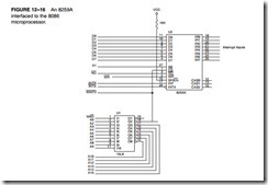
Figure 12–16 shows a single 8259A connected to the microprocessor. Here the SP>EN pin is pulled high to indicate that it is a master. The 8259A is decoded at I/O ports 0400H and 0401H by the PLD (no program shown). Like other peripherals discussed in Chapter 11, the 8259A requires four wait states for it to function properly with a 16 MHz 80386SX and more for some other versions of the Intel microprocessor family.

Cascading Multiple 8259As

Figure 12–17 shows two 8259As connected to the microprocessor in a way that is often found in the ATX-style computer, which has two 8259As for interrupts. The XT- or PC-style computers use a single 8259A controller at interrupt vectors 08H–0FH. The ATX-style computer uses interrupt vector 0AH as a cascade input from a second 8259A located at vectors 70H through 77H. Appendix A contains a table that lists the functions of all the interrupt vectors used.

This circuit uses vectors 08H–0FH and I/O ports 0300H and 0302H for U1, the master; and vectors 70H–77H and I/O ports 0304H and 0306H for U2, the slave. Notice that we also include data bus buffers to illustrate the use of the SP>EN pin on the 8259A. These buffers are used only in very large systems that have many devices connected to their data bus connections. In practice, we seldom find these buffers.

Programming the 8259A

The 8259A is programmed by initialization and operation command words. Initialization command words (ICWs) are programmed before the 8259A is able to function in the system and dictate the basic operation of the 8259A. Operation command words (OCWs) are programmed during the normal course of operation. The OCWs control the operation of the 8259A.

Interrupts-0186

Initialization Command Words. There are four initialization command words (ICWs) for the 8259A that are selected when the A0 pin is a logic 1. When the 8259A is first powered up, it must be sent ICW1, ICW2, and ICW4. If the 8259A is programmed in cascade mode by ICW1, then we also must program ICW3. So if a single 8259A is used in a system, ICW1, ICW2, and ICW4 must be programmed. If cascade mode is used in a system, then all four ICWs must be programmed.

Refer to Figure 12–18 for the format of all four ICWs. The following is a description of each ICW:

ICW1 Programs the basic operation of the 8259A. To program this ICW for 8086–Pentium 4 operation, place a logic 1 in bit IC4. Bits AD1, A7, A6, and A5 are don’t cares for microprocessor operation and only apply to the 8259A when used with an 8-bit 8085 microprocessor (not covered in this textbook). This ICW selects single or cascade operation by programming the SNGL bit. If cascade operation is selected, we must also program ICW3. The LTIM bit determines whether the interrupt request inputs are positive edge-triggered or level-triggered.

ICW2 Selects the vector number used with the interrupt request inputs. For example, if we decide to program the 8259A so it functions at vector locations 08H–0FH, we place 08H into this command word. Likewise, if we decide to program the 8259A for vectors 70H–77H, we place 70H in this ICW.

ICW3 Only used when ICW1 indicates that the system is operated in cascade mode. This ICW indicates where the slave is connected to the master. For example, in Figure 12–18 we connected a slave to IR2. To program ICW3

Interrupts-0187Interrupts-0188

for this connection, in both master and slave, we place 04H in ICW3. Suppose we have two slaves connected to a master using IR0 and IR1. The master is programmed with an ICW3 of 03H; one slave is programmed with an ICW3 of 01H and the other with an ICW3 of 02H.

ICW4 Programmed for use with the 8086–Pentium 4 microprocessors, but is not programmed in a system that functions with the 8085 microprocessor. The rightmost bit must be a logic 1 to select operation with the 8086–Pentium 4 microprocessors, and the remaining bits are programmed as follows:

SFNM—Selects the special fully nested mode of operation for the 8259A if a logic 1 is placed in this bit. This allows the highest priority interrupt request from a slave to be recognized by the master while it is processing another interrupt from a slave. Normally, only one interrupt request is processed at a time and others are ignored until the process is complete.

BUF and M/S—Buffered and master slave are used together to select buffered operation or nonbuffered operation for the 8259A as a master or a slave.

AEOI—Selects automatic or normal end of interrupt (discussed more fully under operation command words). The EOI commands of OCW2 are used only if the AEOI mode is not selected by ICW4. If AEOI is selected, the interrupt automatically resets the interrupt request bit and does not modify priority. This is the preferred mode of operation for the 8259A and reduces the length of the interrupt service procedure.

Operation Command Words. The operation command words (OCWs) are used to direct the operation of the 8259A once it is programmed with the ICW. The OCWs are selected when the A0 pin is at a logic 0 level, except for OCW1, which is selected when A0 is a logic 1. Figure 12–19 lists the binary bit patterns for all three operation command words of the 8259A. Following is a list describing the function of each OCW:

OCW1 Used to set and read the interrupt mask register. When a mask bit is set, it will turn off (mask) the corresponding interrupt input. The mask register is read when OCW1 is read. Because the state of the mask bits is unknown when the 8259A is first initialized, OCW1 must be programmed after programming the ICW upon initialization.

OCW2 Programmed only when the AEOI mode is not selected for the 8259A. In this case, this OCW selects the way that the 8259A responds to an interrupt. The modes are listed as follows:

Nonspecific End-of-Interrupt—A command sent by the interrupt service procedure to signal the end of the interrupt. The 8259A automatically determines which interrupt level was active and resets the correct bit of the interrupt status register. Resetting the status bit allows the interrupt to take action again or a lower priority interrupt to take effect.

Specific End-of-Interrupt—A command that allows a specific interrupt request to be reset. The exact position is determined with bits L2–L0 of OCW2.

Rotate-on-Nonspecific EOI—A command that functions exactly like the Nonspecific End-of-Interrupt command, except that it rotates interrupt priorities after resetting the interrupt status register bit. The level reset by this command becomes the lowest priority interrupt. For example, if IR4 was just serviced by this command, it becomes the lowest priority interrupt input and IR5 becomes the highest priority.

Rotate-on-Automatic EOI—A command that selects automatic EOI with rotating priority. This command must only be sent to the 8259A once if this mode is desired. If this mode must be turned off, use the clear command.

Rotate-on-Specific EOI—Functions as the specific EOI, except that it selects rotating priority.

Set priority—Allows the programmer to set the lowest priority interrupt input using the L2–L0 bits.

Interrupts-0189

OCW3 Selects the register to be read, the operation of the special mask register, and the poll command. If polling is selected, the P bit must be set and then output to the 8259A. The next read operation will read the poll word. The rightmost three bits of the poll word indicate the active interrupt request with the highest priority. The leftmost bit indicates whether there is an interrupt and must be checked to determine whether the rightmost three bits contain valid information.

Status Register. Three status registers are readable in the 8259A: interrupt request register (IRR), in-service register (ISR), and interrupt mask register (IMR). (See Figure 12–20 for all

Interrupts-0190

three status registers; they all have the same bit configuration.) The IRR is an 8-bit register that indicates which interrupt request inputs are active. The ISR is an 8-bit register that contains the level of the interrupt being serviced. The IMR is an 8-bit register that holds the interrupt mask bits and indicates which interrupts are masked off.

Both the IRR and ISR are read by programming OCW3, and IMR is read through OCW1. To read the IMR, A0 = 1; to read either IRR or ISR, A0 = 0. Bit positions D0 and D1 of OCW3 select which register (IRR or ISR) is read when A0 = 0.

8259A Programming Example

Figure 12–21 illustrates the 8259A programmable interrupt controller connected to a 16550 programmable communications controller. In this circuit, the INTR pin from the 16550 is connected to the programmable interrupt controller’s interrupt request input IR0. An IR0 occurs whenever (1) the transmitter is ready to send another character, (2) the receiver has received a character, (3) an error is detected while receiving data, and (4) a modem interrupt occurs. Notice that the 16550

Interrupts-0191

is decoded at I/O ports 40H and 47H, and the 8259A is decoded at 8-bit I/O ports 48H and 49H. Both devices are interfaced to the data bus of an 8088 microprocessor.

Initialization Software. The first portion of the software for this system must program both the 16550 and the 8259A, and then enable the INTR pin on the 8088 so that interrupts can take effect. Example 12–8 lists the software required to program both devices and enable INTR. This software uses two memory FIFOs that hold data for the transmitter and for the receiver. Each memory FIFO is 16K bytes long and is addressed by a pair of pointers (input and output).

Interrupts-0192

The first portion of the procedure (INIT) programs the 16550 UART for operation with seven data bits, odd parity, one stop bit, and a baud rate clock of 9600. The FIFO control register also enables both the transmitter and receiver.

The second part of the procedure programs the 8259A, with its three ICWs and one OCW. The 8259A is set up so that it functions at interrupt vectors 80H–87H and operates with automatic EOI. The OCW enables the interrupt for the 16550 UART. The INTR pin of the micro- processor is also enabled by using the STI instruction.

The final part of the software enables the receiver and error interrupts of the 16550 UART through the interrupt control register. The transmitter interrupt is not enabled until data are avail- able for transmission. See Figure 12–22 for the contents of the interrupt control register of the 16550 UART. Notice that the control register can enable or disable the receiver, transmitter, line status (error), and modem interrupts.

Handling the 16550 UART Interrupt Request. Because the 16550 generates only one interrupt request for various interrupts, the interrupt handler must poll the 16550 to determine what type of interrupt has occurred. This is accomplished by examining the interrupt identification register (see Figure 12–23). Note that the interrupt identification register (read-only) shares the same I/O port as the FIFO control register (write-only).

The interrupt identification register indicates whether an interrupt is pending, the type of interrupt, and whether the transmitter and receiver FIFO memories are enabled. See Table 12–2 for the contents of the interrupt control bits.

The interrupt service procedure must examine the contents of the interrupt identification register to determine what event caused the interrupt and pass control to the appropriate procedure for the event. Example 12–9 shows the first part of an interrupt handler that passes control to RECV for a receiver data interrupt, TRANS for a transmitter data interrupt, and ERR for a line status error interrupt. Note that the modem status is not tested in this example.

Interrupts-0193Interrupts-0194

Receiving data from the 16550 requires two procedures. One procedure reads the data register of the 16550 each time that the INTR pin requests an interrupt and stores it into the memory FIFO. The other procedure reads data from the memory FIFO from the main program.

Example 12–10 lists the procedure used to read data from the memory FIFO from the main program. This procedure assumes that the pointers (IIN and IOUT) are initialized in the initialization dialog for the system (not shown). The READ procedure returns with AL containing a character read from the memory FIFO. If the memory FIFO is empty, the procedure returns with the carry flag bit set to a logic 1. If AL contains a valid character, the carry flag bit is cleared upon return from READ.

Notice how the FIFO is reused by changing the address from the top of the FIFO to the bottom whenever it exceeds the start of the FIFO plus 16K. Notice that interrupts are enabled at the end of this procedure, in case they are disabled by a full memory FIFO condition by the RECV interrupt procedure.

Interrupts-0195

Example 12–11 lists the RECV interrupt service procedure that is called each time the 16550 receives a character for the microprocessor. In this example, the interrupt uses vector type number 80H, which must address the interrupt handler of Example 12–9. Each time that this interrupt occurs, the REVC procedure is accessed by the interrupt handler reading a character from the 16550. The RECV procedure stores the character into the memory FIFO. If the memory FIFO is full, the receiver interrupt is disabled by the interrupt control register within the 16550. This may result in lost data, but at least it will not cause the interrupt to overrun valid data already stored in the memory FIFO. Any error conditions detected by the 8251A store a ? (3FH) in the memory FIFO. Note that errors are detected by the ERR portion of the interrupt handler (not shown).

Interrupts-0196

Transmitting Data to the 16550. Data are transmitted to the 16550 in much the same manner as they are received, except that the interrupt service procedure removes transmit data from a second 16K-byte memory FIFO.

Example 12–12 lists the procedure that fills the output FIFO. It is similar to the procedure listed in Example 12–10, except it determines whether the FIFO is full instead of empty.

Interrupts-0197

Example 12–13 lists the interrupt service subroutine for the 16550 UART transmitter. This procedure is a continuation of the interrupt handler presented in Example 12–9 and is similar to the RECV procedure of Example 12–11, except that it determines whether the FIFO is empty rather than full. Note that we do not include an interrupt service procedure for the break interrupt or any errors.

Interrupts-0198

The 16550 also contains a scratch register, which is a general-purpose register that can be used in any way deemed necessary by the programmer. Also contained in the 16550 are a modem control register and a modem status register. These registers allow the modem to cause interrupt and control the operation of the 16550 with a modem. See Figure 12–24 for the contents of both the modem status register and the modem control register.

The modem control register uses bit positions 0–3 to control various pins on the 16550. Bit position 4 enables the internal loop-back test for testing purposes. The modem status register allows the status of the modem pins to be tested; it also allows the modem pins to be checked for a change or, in the case of RI, a trailing edge.

Figure 12–25 illustrates the 16550 UART, connected to an RS-232C interface that is often used to control a modem. Included in this interface are line driver and receiver circuits used to convert between TTL levels on the 16550 to RS-232C levels found on the interface. Note that RS-232C levels are usually +12 V for a logic 0 and -12 V for a logic 1 level.

In order to transmit or receive data through the modem, the DTR pin is activated (logic 0) and the UART then waits for the DSR pin to become a logic 0 from the modem, indicating that the modem is ready. Once this handshake is complete, the UART sends the modem a logic 0 on the RTS pin. When the modem is ready, it returns the CTS signal (logic 0) to the UART. Communications can now commence. The DCD signal from the modem is an indication that the modem has detected a carrier. This signal must also be tested before communications can begin.


INTERRUPTS:EXPANDING THE INTERRUPT STRUCTURE

EXPANDING THE INTERRUPT STRUCTURE

This text covers three of the more common methods of expanding the interrupt structure of the microprocessor. In this section, we explain how, with software and some hardware modification of the circuit shown in Figure 12–10, it is possible to expand the INTR input so that it accepts seven interrupt inputs. We also explain how to “daisy-chain” interrupts by software polling. In the next section, we describe a third technique in which up to 63 interrupting inputs can be added by means of the 8259A programmable interrupt controller.

Using the 74ALS244 to Expand Interrupts

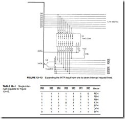
The modification shown in Figure 12–13 allows the circuit of Figure 12–10 to accommodate up to seven additional interrupt inputs. The only hardware change is the addition of an eight-input NAND gate, which provides the INTR signal to the microprocessor when any of the IR inputs becomes active.

Operation. If any of the IR inputs becomes a logic 0, then the output of the NAND gate goes to a logic 1 and requests an interrupt through the INTR input. The interrupt vector that is fetched during the INTA pulse depends on which interrupt request line becomes active. Table 12–1 shows the interrupt vectors used by a single interrupt request input.

If two or more interrupt request inputs are simultaneously active, a new interrupt vector is generated. For example, if IR1 and IR0 are both active, the interrupt vector generated is FCH (252). Priority is resolved at this location. If the IR0 input is to have the higher priority, the vector address for IR0 is stored at vector location FCH. The entire top half of the vector table and its 128 interrupt vectors must be used to accommodate all possible conditions of these seven interrupt request inputs. This seems wasteful, but in many dedicated applications it is a cost-effective approach to interrupt expansion.

Interrupts-0181

Daisy-Chained Interrupt

Expansion by means of a daisy-chained interrupt is in many ways better than using the 74ALS244 because it requires only one interrupt vector. The task of determining priority is left to the interrupt service procedure. Setting priority for a daisy-chain does require additional soft- ware execution time, but in general this is a much better approach to expanding the interrupt structure of the microprocessor.

Figure 12–14 illustrates a set of two 82C55 peripheral interfaces with their four INTR out- puts daisy-chained and connected to the single INTR input of the microprocessor. If any interrupt output becomes a logic 1, so does the INTR input to the microprocessor causing an interrupt.

When a daisy-chain is used to request an interrupt, it is better to pull the data bus connections (D0–D7) high by using pull-up resistors so interrupt vector FFH is used for the chain. Any

Interrupts-0182

interrupt vector can be used to respond to a daisy-chain. In the circuit, any of the four INTR out- puts from the two 82C55s will cause the INTR pin on the microprocessor to go high, requesting an interrupt.

When the INTR pin does go high with a daisy-chain, the hardware gives no direct indication as to which 82C55 or which INTR output caused the interrupt. The task of locating which INTR output became active is up to the interrupt service procedure, which must poll the 82C55s to determine which output caused the interrupt.

Example 12–7 illustrates the interrupt service procedure that responds to the daisy-chain interrupt request. The procedure polls each 82C55 and each INTR output to decide which interrupt service procedure to utilize.

Interrupts-0183Interrupts-0184


INTERRUPTS:BASIC INTERRUPT PROCESSING.

INTERRUPTS

INTRODUCTION

In this chapter, the coverage of basic I/O and programmable peripheral interfaces is expanded by examining a technique called interrupt-processed I/O. An interrupt is a hardware-initiated procedure that interrupts whatever program is currently executing. This chapter provides examples and a detailed explanation of the interrupt structure of the entire Intel family of microprocessors.

CHAPTER OBJECTIVES

Upon completion of this chapter, you will be able to:

1. Explain the interrupt structure of the Intel family of microprocessors.

2. Explain the operation of software interrupt instructions INT, INTO, INT 3, and BOUND.

3. Explain how the interrupt enable flag bit (IF) modifies the interrupt structure.

4. Describe the function of the trap interrupt flag bit (TF) and the operation of trap-generated tracing.

5. Develop interrupt-service procedures that control lower-speed, external peripheral devices.

6. Expand the interrupt structure of the microprocessor by using the 82S9A programmable interrupt controller and other techniques.

7. Explain the purpose and operation of a real-time clock.

BASIC INTERRUPT PROCESSING

In this section, we discuss the function of an interrupt in a microprocessor-based system, and the structure and features of interrupts available to the Intel family of microprocessors.

The Purpose of Interrupts

Interrupts are particularly useful when interfacing I/O devices that provide or require data at relatively low data transfer rates. In Chapter 11, for instance, we showed a keyboard example using strobed input operation of the 82C55. In that example, software polled the 82C55 and its IBF bit to decide whether data were available from the keyboard. If the person using the keyboard typed

Interrupts-0164

one character per second, the software for the 82C55 waited an entire second between each key- stroke for the person to type another key. This process was such a tremendous waste of time that designers developed another process, interrupt processing, to handle this situation.

Unlike the polling technique, interrupt processing allows the microprocessor to execute other software while the keyboard operator is thinking about what key to type next. As soon as a key is pressed, the keyboard encoder debounces the switch and puts out one pulse that interrupts the microprocessor. The microprocessor executes other software until the key is actually pressed, when it reads a key and returns to the program that was interrupted. As a result, the micro- processor can print reports or complete any other task while the operator is typing a document and thinking about what to type next.

Figure 12–1 shows a time line that indicates a typist typing data on a keyboard, a printer removing data from the memory, and a program executing. The program is the main program that is interrupted for each keystroke and each character that is to print on the printer. Note that the keyboard interrupt service procedure, called by the keyboard interrupt, and the printer interrupt service procedure each take little time to execute.

Interrupts

The interrupts of the entire Intel family of microprocessors include two hardware pins that request interrupts (INTR and NMI), and one hardware pin (INTA) that acknowledges the interrupt requested through INTR. In addition to the pins, the microprocessor also has software interrupts INT, INTO, INT 3, and BOUND. Two flag bits, IF (interrupt flag) and TF (trap flag), are also used with the interrupt structure and a special return instruction, IRET (or IRETD in the 80386, 80486, or Pentium–Pentium 4).

Interrupt Vectors. The interrupt vectors and vector table are crucial to an understanding of hardware and software interrupts. The interrupt vector table is located in the first 1024 bytes of memory at addresses 000000H–0003FFH. It contains 256 different four-byte interrupt vectors. An interrupt vector contains the address (segment and offset) of the interrupt service procedure.

Figure 12–2 illustrates the interrupt vector table for the microprocessor. The first five interrupt vectors are identical in all Intel microprocessor family members, from the 8086 to the Pentium. Other interrupt vectors exist for the 80286 that are upward-compatible to the 80386, 80486, and Pentium–Core2, but not downward-compatible to the 8086 or 8088. Intel reserves the first 32 interrupt vectors for their use in various microprocessor family members. The last 224 vectors are available as user interrupt vectors. Each vector is four bytes long in the real mode and contains the starting address of the interrupt service procedure. The first two bytes of the vector contain the offset address and the last two bytes contain the segment address.

The following list describes the function of each dedicated interrupt in the microprocessor:

TYPE 0 The divide error whenever the result from a division overflows or an attempt is made to divide by zero.

TYPE 1 Single-step or trap occurs after the execution of each instruction if the trap (TF) flag bit is set. Upon accepting this interrupt, the TF bit is cleared so that the

Interrupts-0165

interrupt service procedure executes at full speed. (More detail is provided about this interrupt later in this section of the chapter.)

TYPE 2 The non-maskable interrupt occurs when a logic 1 is placed on the NMI input pin to the microprocessor. This input is non-maskable, which means that it cannot be disabled.

TYPE 3 A special one-byte instruction (INT 3) that uses this vector to access its interrupt- service procedure. The INT 3 instruction is often used to store a breakpoint in a program for debugging.

TYPE 4 Overflow is a special vector used with the INTO instruction. The INTO instruction interrupts the program if an overflow condition exists, as reflected by the overflow flag (OF).

TYPE 5 The BOUND instruction compares a register with boundaries stored in the memory. If the contents of the register are greater than or equal to the first word in memory and less than or equal to the second word, no interrupt occurs because the contents of the register are within bounds. If the contents of the register are out of bounds, a type 5 interrupt ensues.

TYPE 6 An invalid opcode interrupt occurs whenever an undefined opcode is encountered in a program.

TYPE 7 The coprocessor not available interrupt occurs when a coprocessor is not found in the system, as dictated by the machine status word (MSW or CR0) coprocessor control bits. If an ESC or WAIT instruction executes and the coprocessor is not found, a type 7 exception or interrupt occurs.

TYPE 8 A double fault interrupt is activated whenever two separate interrupts occur during the same instruction.

TYPE 9 The coprocessor segment overrun occurs if the ESC instruction (coprocessor opcode) memory operand extends beyond offset address FFFFH in real mode.

TYPE 10 An invalid task state segment interrupt occurs in the protected mode if the TSS is invalid because the segment limit field is not 002BH or higher. In most cases, this is caused because the TSS is not initialized.

TYPE 11 The segment not present interrupt occurs when the protected mode P bit (P = 0) in a descriptor indicates that the segment is not present or not valid.

TYPE 12 A stack segment overrun occurs if the stack segment is not present (P = 0) in the protected mode or if the limit of the stack segment is exceeded.

TYPE 13 The general protection fault occurs for most protection violations in the 80286–Core2 protected mode system. (These errors occur in Windows as general protection faults.) A list of these protection violations follows:

(a) Descriptor table limit exceeded

(b) Privilege rules violated

(c) Invalid descriptor segment type loaded

(d) Write to code segment that is protected

(e) Read from execute-only code segment

(f) Write to read-only data segment

(g) Segment limit exceeded

(h) CPL = IOPL when executing CTS, HLT, LGDT, LIDT, LLDT, LMSW, or LTR

(i) CPL > IOPL when executing CLI, IN, INS, LOCK, OUT, OUTS, and STI

TYPE 14 Page fault interrupts occur for any page fault memory or code access in the 80386, 80486, and Pentium–Core2 microprocessors.

TYPE 16 Coprocessor error takes effect whenever a coprocessor error (ERROR = 0) occurs for the ESCape or WAIT instructions for the 80386, 80486, and Pentium–Core2 microprocessors only.

TYPE 17 Alignment checks indicate that word and doubleword data are addressed at an odd memory location (or an incorrect location, in the case of a doubleword). This interrupt is active in the 80486 and Pentium–Core2 microprocessors.

TYPE 18 A machine check activates a system memory management mode interrupt in the Pentium–Core2 microprocessors.

Interrupt Instructions: BOUND, INTO, INT, INT 3, and IRET

Of the five software interrupt instructions available to the microprocessor, INT and INT 3 are very similar, BOUND and INTO are conditional, and IRET is a special interrupt return instruction.

The BOUND instruction, which has two operands, compares a register with two words of memory data. For example, if the instruction BOUND AX,DATA is executed, AX is compared with the contents of DATA and DATA+1 and also with DATA+2 and DATA+3. If AX is less than the contents of DATA and DATA+1, a type 5 interrupt occurs. If AX is greater than DATA+2 and DATA+3, a type 5 interrupt occurs. If AX is within the bounds of these two memory words, no interrupt occurs.

The INTO instruction checks or tests the overflow flag (O). If O = 1, the INTO instruction calls the procedure whose address is stored in interrupt vector type number 4. If O = 0, then the INTO instruction performs no operation and the next sequential instruction in the program executes.

The INT n instruction calls the interrupt service procedure that begins at the address represented in vector number n. For example, an INT 80H or INT 128 calls the interrupt service procedure whose address is stored in vector type number 80H (000200H–00203H). To determine the vector address, just multiply the vector type number (n) by 4, which gives the beginning address of the four-byte long interrupt vector. For example, INT 5 = 4 × 5 or 20 (14H). The vector for INT 5 begins at address 0014H and continues to 0017H. Each INT instruction is stored in two bytes of memory: The first byte contains the opcode, and the second byte contains the interrupt type number. The only exception to this is the INT 3 instruction, a one-byte instruction. The INT 3 instruction is often used as a breakpoint-interrupt because it is easy to insert a one-byte instruction into a program. Breakpoints are often used to debug faulty software.

The IRET instruction is a special return instruction used to return for both software and hardware interrupts. The IRET instruction is much like a far RET, because it retrieves the return address from the stack. It is unlike the near return because it also retrieves a copy of the flag register from the stack. An IRET instruction removes six bytes from the stack: two for the IP, two for the CS, and two for the flags.

In the 80386–Core2, there is also an IRETD instruction because these microprocessors can push the EFLAG register (32 bits) on the stack, as well as the 32-bit EIP in the protected mode and 16-bit code segment register. If operated in the real mode, we use the IRET instruction with the 80386–Core2 microprocessors. If the Pentium 4 operates in 64-bit mode, an IRETQ instruction is used to return from an interrupt. The IRETQ instruction pops the EFLAG register into RFLAGS and also the 64-bit return address is placed into the RIP register.

The Operation of a Real Mode Interrupt

When the microprocessor completes executing the current instruction, it determines whether an interrupt is active by checking (1) instruction executions, (2) single-step, (3) NMI, (4) coprocessor segment overrun, (5) INTR, and (6) INT instructions in the order presented. If one or more of these interrupt conditions are present, the following sequence of events occurs:

1. The contents of the flag register are pushed onto the stack.

2. Both the interrupt (IF) and trap (TF) flags are cleared. This disables the INTR pin and the trap or single-step feature.

3. The contents of the code segment register (CS) are pushed onto the stack.

4. The contents of the instruction pointer (IP) are pushed onto the stack.

5. The interrupt vector contents are fetched, and then placed into both IP and CS so that the next instruction executes at the interrupt service procedure addressed by the vector.

Whenever an interrupt is accepted, the microprocessor stacks the contents of the flag register, CS and IP; clears both IF and TF; and jumps to the procedure addressed by the interrupt vector. After the flags are pushed onto the stack, IF and TF are cleared. These flags are returned to the state prior to the interrupt when the IRET instruction is encountered at the end of the interrupt service procedure. Therefore, if interrupts were enabled prior to the interrupt service procedure, they are automatically re-enabled by the IRET instruction at the end of the procedure.

The return address (in CS and IP) is pushed onto the stack during the interrupt. Sometimes the return address points to the next instruction in the program; sometimes it points to the instruction or point in the program where the interrupt occurred. Interrupt type numbers 0, 5, 6, 7, 8, 10, 11, 12, and 13 push a return address that points to the offending instruction, instead of to the next instruction in the program. This allows the interrupt service procedure to possibly retry the instruction in certain error cases.

Some of the protected mode interrupts (types 8, 10, 11, 12, and 13) place an error code on the stack following the return address. The error code identifies the selector that caused the interrupt. In cases where no selector is involved, the error code is a 0.

Operation of a Protected Mode Interrupt

In the protected mode, interrupts have exactly the same assignments as in the real mode, but the interrupt vector table is different. In place of interrupt vectors, protected mode uses a set of 256 interrupt descriptors that are stored in an interrupt descriptor table (IDT). The interrupt descriptor table is 256 × 8 (2K) bytes long, with each descriptor containing eight bytes. The interrupt descriptor table is located at any memory location in the system by the interrupt descriptor table address register (IDTR).

Each entry in the IDT contains the address of the interrupt service procedure in the form of a segment selector and a 32-bit offset address. It also contains the P bit (present) and DPL bits to describe the privilege level of the interrupt. Figure 12–3 shows the contents of the interrupt descriptor.

Real mode interrupt vectors can be converted into protected mode interrupts by copying the interrupt procedure addresses from the interrupt vector table and converting them to 32-bit offset addresses that are stored in the interrupt descriptors. A single selector and segment descriptor can be placed in the global descriptor table that identifies the first 1M byte of memory as the interrupt segment.

Other than the IDT and interrupt descriptors, the protected mode interrupt functions like the real mode interrupt. We return from both interrupts by using the IRET or IRETD instruction. The only difference is that in protected mode the microprocessor accesses the IDT instead of the

Interrupts-0166Interrupts-0167

interrupt vector table. In the 64-bit mode of the Pentium 4 and Core2, an IRETQ must be used to return from an interrupt. This is one reason why there are different drivers and operating systems for the 64-bit mode.

Interrupt Flag Bits

The interrupt flag (IF) and the trap flag (TF) are both cleared after the contents of the flag register are stacked during an interrupt. Figure 12–4 illustrates the contents of the flag register and the location of IF and TF. When the IF bit is set, it allows the INTR pin to cause an interrupt; when the IF bit is cleared, it prevents the INTR pin from causing an interrupt. When TF = 1, it causes a trap interrupt (type number 1) to occur after each instruction executes. This is why we often call trap a single-step. When TF = 0, normal program execution occurs. This flag bit allows debugging, as explained in Chapters 17 through 19, which detail the 80386–Core2.

The interrupt flag is set and cleared by the STI and CLI instructions, respectively. There are no special instructions that set or clear the trap flag. Example 12–1 shows an interrupt service procedure that turns tracing on by setting the trap flag bit on the stack from inside the procedure. Example 12–2 shows an interrupt service procedure that turns tracing off by clearing the trap flag on the stack from within the procedure.

Interrupts-0168

In both examples, the flag register is retrieved from the stack by using the BP register, which, by default, addresses the stack segment. After the flags are retrieved, the TF bit is either set (TRON) or clears (TROFF) before returning from the interrupt service procedure. The IRET instruction restores the flag register with the new state of the trap flag.

Trace Procedure. Assuming that TRON is accessed by an INT 40H instruction and TROFF is accessed by an INT 41H instruction, Example 12–3 traces through a program immediately fol- lowing the INT 40H instruction. The interrupt service procedure illustrated in Example 12–3 responds to interrupt type number 1 or a trap interrupt. Each time that a trap occurs—after each instruction executes following INT 40H—the TRACE procedure stores the contents of all the 32-bit microprocessor registers in an array called REGS. This provides a register trace of all the instructions between the INT 40H (TRON) and INT 41H (TROFF) if the contents of the registers stored in the array are saved.

Interrupts-0169

Storing an Interrupt Vector in the Vector Table

In order to install an interrupt vector—sometimes called a hook—the assembler must address absolute memory. Example 12–4 shows how a new vector is added to the interrupt vector table by using the assembler and a DOS function call. Here, the vector for INT 40H, for interrupt procedure NEW40, is installed in memory at real mode vector location 100H–103H. The first thing accomplished by the procedure is that the old interrupt vector contents are saved in case we need to uninstall the vector. This step can be skipped if there is no need to uninstall the interrupt.

The function AX = 3100H for INT 21H, the DOS access function, installs the NEW40 procedure in memory until the computer is shut off. The number in DX is the length of the software in paragraphs (16-byte chunks). Refer to Appendix A for more detail about this DOS function.

Notice that the INT40 function has an IRET instruction before ENDP. This is required because the assembler has no way of determining if the FAR procedure is an interrupt procedure. Normal FAR procedures do not need a return instruction, but an interrupt procedure does need an IRET. Interrupts must always be defined as FAR.

Interrupts-0170Interrupts-0171


QUESTIONS AND PROBLEMS ON BASIC I/O INTERFACE.

QUESTIONS AND PROBLEMS

1. Explain which way the data flow for an IN and an OUT instruction.

2. Where is the I/O port number stored for a fixed I/O instruction?

3. Where is the I/O port number stored for a variable I/O instruction?

4. Where is the I/O port number stored for a string I/O instruction?

5. To which register are data input by the 16-bit IN instruction?

6. Describe the operation of the OUTSB instruction.

7. Describe the operation of the INSW instruction.

8. Contrast a memory-mapped I/O system with an isolated I/O system.

9. What is the basic input interface?

10. What is the basic output interface?

11. Explain the term handshaking as it applies to computer I/O systems.

12. An even-number I/O port address is found in the ____________ I/O bank in the 8086 microprocessor.

13. In the Pentium 4, what bank contains I/O port number 000AH?

14. How many I/O banks are found in the Pentium 4 or Core2 microprocessor?

15. Show the circuitry that generates the upper and lower I/O write strobes.

16. What is the purpose of a contact bounce eliminator?

17. Develop an interface to correctly drive a relay. The relay is 12 V and requires a coil current of 150 mA.

18. Develop a relay coil driver that can control a 5.0 V relay that requires 60 mA of coil current.

19. Develop an I/O port decoder, using a 74ALS138, that generates low-bank I/O strobes, for a 16-bit microprocessor, for the following 8-bit I/O port addresses: 10H, 12H, 14H, 16H, 18H, 1AH, 1CH, and 1EH.

20. Develop an I/O port decoder, using a 74ALS138, that generates high-bank I/O strobes, for a 16-bit microprocessor, for the following 8-bit I/O port addresses: 11H, 13H, 15H, 17H, 19H, 1BH, 1DH, and 1FH.

21. Develop an I/O port decoder, using a PLD, that generates 16-bit I/O strobes for the following 16-bit I/O port addresses: 1000H–1001H, 1002H–103H, 1004H–1005H, 1006H–1007H,1008H–1009H, 100AH–100BH, 100CH–100DH, and 100EH–100FH.

22. Develop an I/O port decoder, using a PLD, that generates the following low-bank I/O strobes: 00A8H, 00B6H, and 00EEH.

23. Develop an I/O port decoder, using a PLD, that generates the following high-bank I/O strobes: 300DH, 300BH, 1005H, and 1007H.

24. Why are both BHE and BLE (A0) ignored in a 16-bit port address decoder?

25. An 8-bit I/O device, located at I/O port address 0010H, is connected to which data bus connections in a Pentium 4?

26. An 8-bit I/O device, located at I/O port address 100DH, is connected to which data bus connections in a Core2 microprocessor?

27. The 82C55 has how many programmable I/O pin connections?

28. List the pins that belong to group A and to group B in the 82C55.

29. Which two 82C55 pins accomplish internal I/O port address selection?

30. The RD connection on the 82C55 is attached to which 8086 system control bus connection?

31. Using a PLD, interface an 82C55 to the 8086 microprocessor so that it functions at I/O locations 0380H, 0382H, 0384H, and 0386H.

32. When the 82C55 is reset, its I/O ports are all initialized as .

33. What three modes of operation are available to the 82C55?

34. What is the purpose of the STB signal in strobed input operation of the 82C55?

35. Develop a time delay procedure for the 2.0 GHz Pentium 4 that waits for 80 μs.

36. Develop a time delay procedure for the 3.0 GHz Pentium 4 that waits for 12 ms.

37. Explain the operation of a simple four-coil stepper motor.

38. What sets the IBF pin in strobed input operation of the 82C55?

39. Write the software required to place a logic 1 on the PC7 pin of the 82C55 during strobed input operation.

40. How is the interrupt request pin (INTR) enabled in the strobed input mode of operation of the 82C55?

41. In strobed output operation of the 82C55, what is the purpose of the ACK signal?

42. What clears the OBF signal in strobed output operation of the 82C55?

43. Write the software required to decide whether PC4 is a logic 1 when the 82C55 is operated in the strobed output mode.

44. Which group of pins is used during bidirectional operation of the 82C55?

45. Which pins are general-purpose I/O pins during mode 2 operation of the 82C55?

46. Describe how the display is cleared in the LCD display.

47. How is a display position selected in the LCD display?

48. Write a short procedure that places an ASCII null string in display position 6 on the LCD display.

49. How is the busy flag tested in the LCD display?

50. What changes must be made to Figure 11–25 so that it functions with a keyboard matrix that contains three rows and five columns?

51. What time is usually used to debounce a keyboard?

52. Develop the interface to a three- by four-key telephone-style keypad. You will need to use a lookup table to convert to the proper key code.

53. The 8254 interval timer functions from DC to Hz.

54. Each counter in the 8254 functions in how many different modes?

55. Interface an 8254 to function at I/O port addresses XX10H, XX12H, XX14H, and XX16H.

56. Write the software that programs counter 2 to generate an 80 KHz square wave if the CLK input to counter 2 is 8 MHz.

57. What number is programmed in an 8254 counter to count 300 events?

58. If a 16-bit count is programmed into the 8254, which byte of the count is programmed first?

59. Explain how the read-back control word functions in the 8254.

60. Program counter 1 of the 8254 so that it generates a continuous series of pulses that have a high time of 100 μs and a low time of 1 μs. Make sure to indicate the CLK frequency required for this task.

61. Why does a 50% duty cycle cause the motor to stand still in the motor speed and direction control circuit presented in this chapter?

62. What is asynchronous serial data?

63. What is baud rate?

64. Program the 16550 for operation using six data bits, even parity, one stop bit, and a baud rate of 19,200 using a 18.432 MHz clock. (Assume that the I/O ports are numbered 20H and 22H.)

65. If the 16550 is to generate a serial signal at a baud rate of 2400 baud and the baud rate divisor is programmed for 16, what is the frequency of the signal?

66. Describe the following terms: simplex, half-duplex, and full-duplex.

67. How is the 16550 reset?

68. Write a procedure for the 16550 that transmits 16 bytes from a small buffer in the data segment address (DS is loaded externally) by SI (SI is loaded externally).

69. The DAC0830 converts an 8-bit digital input to an analog output in approximately .

70. What is the step voltage at the output of the DAC0830 if the reference voltage is -2.55 V?

71. Interface a DAC0830 to the 8086 so that it operates at I/O port 400H.

72. Develop a program for the interface of question 71 so the DAC0830 generates a triangular voltage wave-form. The frequency of this wave-form must be approximately 100 Hz.

73. The ADC080X requires approximately to convert an analog voltage into a digital code.

74. What is the purpose of the INTR pin on the ADC080X?

75. The WR pin on the ADC080X is used for what purpose?

76. Interface an ADC080X at I/O port 0260H for data and 0270H to test the INTR pin.

77. Develop a program for the ADC080X in question 76 so that it reads an input voltage once per 100 ms and stores the results in a memory array that is 100H bytes long.

78. Rewrite Example 11–29 using C++ with inline assembly code.


SUMMARY OF BASIC I/O INTERFACE.

SUMMARY

1. The 8086–Core2 microprocessors have two basic types of I/O instructions: IN and OUT. The IN instruction inputs data from an external I/O device into either the AL (8-bit) or AX (16-bit) register. The IN instruction is available as a fixed port instruction, a variable port instruction, or a string instruction (80286–Pentium 4) INSB or INSW. The OUT instruction outputs data from AL or AX to an external I/O device and is available as a fixed, variable, or string instruction OUTSB or OUTSW. The fixed port instruction uses an 8-bit I/O port address, while the variable and string I/O instructions use a 16-bit port number found in the DX register.

2. Isolated I/O, sometimes called direct I/O, uses a separate map for the I/O space, freeing the entire memory for use by the program. Isolated I/O uses the IN and OUT instructions to transfer data between the I/O device and the microprocessor. The control structure of the isolated I/O map uses IORC (I/O read control) and IOWC (I/O write control), plus the bank selection signals BHE and BLE (A0 on the 8086 and 80286), to effect the I/O transfer. The early 8086/8088 used the M/IO (IO/M) signal with RD and WR to generate the I/O control signals.

3. Memory-mapped I/O uses a portion of the memory space for I/O transfers. This reduces the amount of memory available, but it negates the need to use the IORC and IOWC signals for I/O transfers. In addition, any instruction that addresses a memory location using any addressing mode can be used to transfer data between the microprocessor and the I/O device using memory-mapped I/O.

4. All input devices are buffered so that the I/O data are connected only to the data bus during the execution of the IN instruction. The buffer is either built into a programmable peripheral or located separately.

5. All output devices use a latch to capture output data during the execution of the OUT instruction. This is necessary because data appear on the data bus for less than 100 ns for an OUT instruction, and most output devices require the data for a longer time. In many cases, the latch is built into the peripheral.

6. Handshaking or polling is the act of two independent devices synchronizing with a few control lines. For example, the computer asks a printer if it is busy by inputting the BUSY signal from the printer. If it isn’t busy, the computer outputs data to the printer and informs the printer that data are available with a data strobe (DS) signal. This communication between the computer and the printer is a handshake or a poll.

7. Interfaces are required for most switch-based input devices and for most output devices that are not TTL-compatible.

8. The I/O port number appears on address bus connections A7–A0 for a fixed port I/O instruction and on A15–A0 for a variable port I/O instruction (note that A15–A8 contains zeros for an 8-bit port). In both cases, address bits above A15 are undefined.

9. Because the 8086/80286/80386SX microprocessors contain a 16-bit data bus and the I/O addresses reference byte-sized I/O locations, the I/O space is also organized in banks, as is the memory system. In order to interface an 8-bit I/O device to the 16-bit data bus, we often require separate write strobes (an upper and a lower) for I/O write operations. Likewise, the 80486 and Pentium–Core2 also have I/O arranged in banks.

10. The I/O port decoder is much like the memory address decoder, except instead of decoding the entire address, the I/O port decoder decodes only a l6-bit address for variable port instructions and often an 8-bit port number for fixed I/O instructions.

11. The 82C55 is a programmable peripheral interface (PIA) that has 24 I/O pins that are programmable in two groups of 12 pins each (group A and group B). The 82C55 operates in three modes: simple I/O (mode 0), strobed I/O (mode 1), and bidirectional I/O (mode 2). When the 82C55 is interfaced to the 8086 operating at 8 MHz, we insert two wait states because the speed of the microprocessor is faster than the 82C55 can handle.

12. The LCD display device requires a fair amount of software, but it displays ASCII-coded information.

13. The 8254 is a programmable interval timer that contains three l6-bit counters that count in binary or binary-coded decimal (BCD). Each counter is independent and operates in six different modes: (1) events counter, (2) retriggerable, monostable multivibrator, (3) pulse generator, (4) square-wave generator, (5) software-triggered pulse generator, and (6) hardware- triggered pulse generator.

14. The 16550 is a programmable communications interface, capable of receiving and transmitting asynchronous serial data.

15. The DAC0830 is an 8-bit digital-to-analog converter that converts a digital signal to an analog voltage within 1.0 μs.

16. The ADC0804 is an 8-bit analog-to-digital converter that converts an analog signal into a digital signal within 100 μs.