THE ARITHMETIC COPROCESSOR, MMX, AND SIMD TECHNOLOGIES:PROGRAMMING WITH THE ARITHMETIC COPROCESSOR.

PROGRAMMING WITH THE ARITHMETIC COPROCESSOR

This section of the chapter provides programming examples for the arithmetic coprocessor. Each example is chosen to illustrate a programming technique for the coprocessor.

Calculating the Area of a Circle

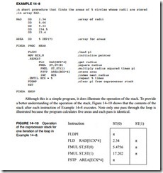
This first programming example illustrates a simple method of addressing the coprocessor stack. First, recall that the equation for calculating the area of a circle is A = πR2. A program that per- forms this calculation is listed in Example 14–8. Note that this program takes test data from array RAD that contains five sample radii. The five areas are stored in a second array called AREA. No attempt is made in this program to use the data from the AREA array.

The Arithmetic Coprocessor, MMX,and SIMD Technologies-0287

The first instruction loads π to the top of the stack. Next, the contents of memory location RAD [ECX*4], one of the elements of the array, is loaded to the top of the stack. This pushes π to ST(1). Next, the FMUL ST,ST(0) instruction squares the radius on the top of the stack. The FMUL ST,ST(1) instruction forms the area. Finally, the top of the stack is stored in the AREA array and also pops it from the stack in preparation for the next iteration.

Notice how care is taken to always remove all stack data. The last instruction before the RET pops π from the stack. This is important because if data remain on the stack at the end of the procedure, the stack top will no longer be register 0. This could cause problems because software assumes that the top of the stack is register 0. Another way of ensuring that the coprocessor is initialized is to place the FINIT (initialization) instruction at the start of the program.

Finding the Resonant Frequency

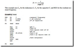
An equation commonly used in electronics is the formula for determining the resonant frequency of an LC circuit. The equation solved by the program illustrated in Example 14–9 is


This example uses L1 for the inductance L, C1 for the capacitor C, and RES for the resultant res- onant frequency.

The Arithmetic Coprocessor, MMX,and SIMD Technologies-0288

Notice the straightforward manner in which the program solves this equation. Very little extra data manipulation is required because of the stack inside the coprocessor. Notice how FDIVR, using classic stack addressing, is used to form the reciprocal. If you own a reverse Polish notation calculator, such as those produced by Hewlett-Packard, you are familiar with stack addressing. If not, using the coprocessor will increase your experience with this type of entry.

Finding the Roots Using the Quadratic Equation

This example illustrates how to find the roots of a polynomial expression (ax2 + bx + c = 0) by using the quadratic equation. The quadratic equation is:

The Arithmetic Coprocessor, MMX,and SIMD Technologies-0289

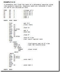
Example 14–10 illustrates a program that finds the roots (R1 and R2) for the quadratic equation. The constants are stored in memory locations A1, B1, and C1. Note that no attempt is made to determine the roots if they are imaginary. This example tests for imaginary roots and then exits to DOS with a zero in the roots (R1 and R2), if it finds them. In practice, imaginary roots could be solved for and stored in a separate set of result memory locations.

The Arithmetic Coprocessor, MMX,and SIMD Technologies-0290

Using a Memory Array to Store Results

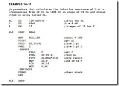
The next programming example illustrates the use of a memory array and the scaled-indexed addressing mode to access the array. Example 14–11 shows a program that calculates 100 values of inductive reactance. The equation for inductive reactance is XL = 2πFL. In this example, the frequency range is from 10 Hz to 1000 Hz for F and an inductance of 4 mH. Notice how the instruction FSTP XL[ECX*4 + 4] is used to store the reactance for each frequency, beginning with the last at 1000 Hz and ending with the first at 10 Hz. Also notice how the FCOMP instruction is used to clear the stack just before the RET instruction.

The Arithmetic Coprocessor, MMX,and SIMD Technologies-0291

Converting a Single-Precision Floating-Point Number to a String

This section of the text shows how to take the floating-point contents of a 32-bit single-precision floating-point number and store it as an ASCII character string. The procedure converts the floating-point number as a mixed number with an integer part and a fractional part, separated by a decimal point. In order to simplify the procedure, a limit is placed on the size of the mixed number so the integer portion is a 32-bit binary number (±2 G) and the fraction is a 24-bit binary number (1/16M). The procedure will not function properly for larger or smaller numbers.

Example 14–12 lists a procedure that converts the contents of memory location NUMB to a string stored in the STR array. The procedure first tests the sign of the number and stores a minus sign for a negative number. After storing a minus sign, if needed, the number is made positive by the FABS instruction. Next, it is divided into an integer and fractional part and stored at WHOLE and FRACT. Notice how the FRNDINT instruction is used to round (using the chop mode) the top of the stack to form the whole number part of NUMB. The whole number part is then subtracted from the original number to generate the fractional part. This is accomplished with the FSUB instruction that subtracts the contents of ST(1) from ST.

The Arithmetic Coprocessor, MMX,and SIMD Technologies-0292The Arithmetic Coprocessor, MMX,and SIMD Technologies-0293


THE ARITHMETIC COPROCESSOR, MMX, AND SIMD TECHNOLOGIES:INSTRUCTION SET

INSTRUCTION SET

The arithmetic coprocessor executes over 68 different instructions. Whenever a coprocessor instruction references memory, the microprocessor automatically generates the memory address for the instruction. The coprocessor uses the data bus for data transfers during coprocessor instructions and the microprocessor uses it during normal instructions. Also note that the 80287 uses the Intel-reserved I/O ports 00F8H–00FFH for communications between the coprocessor and the microprocessor (even though the coprocessor only uses ports 00FCH–00FFH). These ports are used mainly for the FSTSW AX instruction. The 80387–Core2 use I/O ports 800000F8H–800000FFH for these communications.

This section of the text describes the function of each instruction and lists its assembly language form. Because the coprocessor uses the microprocessor memory-addressing modes, not all forms of each instruction are illustrated. Each time that the assembler encounters a coprocessor mnemonic opcode, it converts it into a machine language ESC instruction. The ESC instruction represents an opcode to the coprocessor.

Data Transfer Instructions

There are three basic data transfers: floating-point, signed integer, and BCD. The only time that data ever appear in the signed integer or BCD form is in the memory. Inside the coprocessor, data are always stored as an 80-bit extended-precision floating-point number.

Floating-Point Data Transfers. There are four traditional floating-point data transfer instructions in the coprocessor instruction set: FLD (load real), FST (store real), FSTP (store real and pop), and FXCH (exchange). A new instruction is added to the Pentium Pro through Core2 called a conditional floating-point move instruction that uses the opcode FCMOV with a floating-point condition.

The FLD instruction loads floating-point memory data to the top of the internal stack, referred to as ST (stack top). This instruction stores the data on the top of the stack and then decrements the stack pointer by 1. Data loaded to the top of the stack are from any memory location or from another coprocessor register. For example, an FLD ST(2) instruction copies the con- tents of register 2 to the stack top, which is ST. The top of the stack is register 0 when the coprocessor is reset or initialized. Another example is the FLD DATA7 instruction, which copies the contents of memory location DATA 7 to the top of the stack. The size of the transfer is auto- matically determined by the assembler through the directives DD or REAL4 for single-precision, DQ or REAL 8 for double-precision, and DT or REAL10 for extended temporary-precision.

The FST instruction stores a copy of the top of the stack into the memory location or coprocessor register indicated by the operand. At the time of storage, the internal, extended temporary-precision floating-point number is rounded to the size of the floating-point number indicated by the control register.
The Arithmetic Coprocessor, MMX,and SIMD Technologies-0265

The FSTP (floating-point store and pop) instruction stores a copy of the top of the stack into memory or any coprocessor register, and then pops the data from the top of the stack. You might think of FST as a copy instruction and FSTP as a removal instruction.

The FXCH instruction exchanges the register indicated by the operand with the top of the stack. For example, the FXCH ST(2) instruction exchanges the top of the stack with register 2.

Integer Data Transfer Instructions. The coprocessor supports three integer data transfer instructions: FILD (load integer), FIST (store integer), and FISTP (store integer and pop). These three instructions function as did FLD, FST, and FSTP, except that the data transferred are integer data. The coprocessor automatically converts the internal extended temporary-precision floating-point data to integer data. The size of the data is determined by the way that the label is defined with DW, DD, or DQ in the assembly language program.

BCD Data Transfer Instructions. Two instructions load or store BCD signed-integer data. The FBLD instruction loads the top of the stack with BCD memory data, and the FBSTP stores the top of the stack and does a pop.

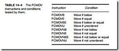
The Pentium Pro through Pentium 4 FCMOV Instruction. The Pentium Pro–Pentium 4 micro- processors contain a new instruction called FCMOV, which also contains a condition. If the condition is true, the FCMOV instruction copies the source to the destination. The conditions tested by FCMOV and the opcodes used with FCMOV appear in Table 14–4. Notice that these conditions check for either an ordered or unordered condition. The testing for NAN and denormalized numbers are not checked with FCMOV.

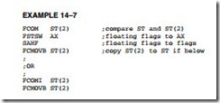
Example 14–7 shows how the FCMOVB (move if below) instruction is used to copy the contents of ST(2) to the stack top (ST) if the contents of ST(2) is below ST. Notice that the FCOM instruction must be used to perform the compare and the contents of the status register must still be copied to the flags for this instruction to function. More about the FCMOV instruction appears with the FCOMI instruction, which is also new to the Pentium Pro through the Core2 microprocessors.
The Arithmetic Coprocessor, MMX,and SIMD Technologies-0266The Arithmetic Coprocessor, MMX,and SIMD Technologies-0267

Arithmetic Instructions

Arithmetic instructions for the coprocessor include addition, subtraction, multiplication, division, and calculating square roots. The arithmetic-related instructions are scaling, rounding, absolute value, and changing the sign.

Table 14–5 shows the basic addressing modes allowed for the arithmetic operations. Each addressing mode is shown with an example using the FADD (real addition) instruction. All arithmetic operations are floating-point, except some cases in which memory data are referenced as an operand.

The classic stack form of addressing operand data (stack addressing) uses the top of the stack as the source operand and the next to the top of the stack as the destination operand. Afterward, a pop removes the source datum from the stack and only the result in the destination register remains at the top of the stack. To use this addressing mode, the instruction is placed in the program without any operands such as FADD or FSUB. The FADD instruction adds ST to ST(1) and stores the answer at the top of the stack; it also removes the original two data from the stack by popping. Note carefully that FSUB subtracts ST from ST(1) and leaves the difference at ST. Therefore, a reverse subtraction (FSUBR) subtracts ST(1) from ST and leaves the difference at ST. (Note that an error exists in Intel documentation, including the Pentium data book, which describes the operation of some reverse instructions.) Another use for reverse operations is for finding a reciprocal (1/X). This is accomplished, if X is at the top of the stack, by loading a 1.0 to ST, followed by the FDIVR instruction. The FDIVR instruction divides ST(1) into ST or X into 1 and leaves the reciprocal (1/X) at ST.

The register-addressing mode uses ST for the top of the stack and ST(n) for another loca- tion, where n is the register number. With this form, one operand must be ST and the other is ST(n). Note that to double the top of the stack, the FADD ST,ST(0) instruction is used where ST(0) also addresses the top of the stack. One of the two operands in the register-addressing mode must be ST, while the other must be in the form ST(n), where n is a stack register 0–7. For many instructions, either ST or ST(n) can be the destination. It is fairly important that the top of the stack be ST(0). This is accomplished by resetting or initializing the coprocessor before using it in a program. Another example of register-addressing is FADD ST(1),ST where the contents of ST are added to ST(1) and the result is placed in ST(1).

The top of the stack is always used as the destination for the memory-addressing mode because the coprocessor is a stack-oriented machine. For example, the FADD DATA instruction adds the real number contents of memory location DATA to the top of the stack.

Arithmetic Operations. The letter P in an opcode specifies a register pop after the operation (FADDP compared to FADD). The letter R in an opcode (subtraction and division only) indicates reverse mode. The reverse mode is useful for memory data because memory data normally subtract from the top of the stack. A reversed subtract instruction subtracts the top of the stack from memory and stores the result in the top of the stack. For example, if the top of the stack contains a 10 and memory location DATAl contains a 1, the FSUB DATA1 instruction results in a +9 on the stack top, and the FSUBR instruction results in a –9. Another example is FSUBR ST,ST(1), which will subtract ST from ST(1) and store the result on ST. A variant is FSUBR ST(1),ST, which will subtract ST(1) from ST and store the result on ST(1).

The letter I as a second letter in an opcode indicates that the memory operand is an integer. For example, the FADD DATA instruction is a floating-point addition, while the FIADD DATA is an integer addition that adds the integer at memory location DATA to the floating- point number at the top of the stack. The same rules apply to FADD, FSUB, FMUL, and FDIV instructions.

Arithmetic-Related Operations. Other operations that are arithmetic in nature include FSQRT (square root), FSCALE (scale a number), FPREM/FPREM1 (find partial remainder), FRNDINT (round to integer), FXTRACT (extract exponent and significand), FABS (find absolute value), and FCHG (change sign). These instructions and the functions that they per- form follow:

FSQRT Finds the square root of the top of the stack and leaves the resultant square root at the top of the stack. An invalid error occurs for the square root of a negative number. For this reason, the IE bit of the status register should be tested whenever an invalid result can occur. The IE bit can be tested by loading the status register to AX with the FSTSW AX instruction, followed by TEST AX,1 to test the IE status bit.

FSCALE Adds the contents of ST(1) (interpreted as an integer) to the exponent at the top of the stack. FSCALE multiplies or divides rapidly by powers of two. The value in ST(1) must be between 2–15 and 2+15.

FPREM/FPREM1 Performs modulo division of ST by ST(1). The resultant remainder is found in the top of the stack and has the same sign as the original div dend. Note that a modulo division results in a remainder without a quotient. Note also that FPREM is supported for the 8086 and 80287, and FPREM1 should be used in newer coprocessors.

FRNDINT Rounds the top of the stack to an integer.

FXTRACT Decomposes the number at the top of the stack into two separate parts that represent the value of the unbiased exponent and the value of the significand. The extracted significand is found at the top of the stack and the unbiased exponent at ST(1). This instruction is often used to convert a floating-point number into a form that can be printed as a mixed number.

FABS Changes the sign of the top of the stack to positive.

FCHS Changes the sign from positive to negative or negative to positive.

Comparison Instructions

The comparison instructions all examine data at the top of the stack in relation to another element and return the result of the comparison in the status register condition code bits C3–C0. Comparisons that are allowed by the coprocessor are FCOM (floating-point compare), FCOMP (floating-point compare with a pop), FCOMPP (floating-point compare with two pops), FICOM (integer compare), FICOMP (integer compare and pop), FSTS (test), and FXAM (examine). New with the introduction of the Pentium Pro is the floating compare and move

results to flags or FCOMI instruction. Following is a list of these instructions with a description of their functions:

FCOM Compares the floating-point data at the top of the stack with an operand, which may be any register or any memory operand. If the operand is not coded with the instruction, the next stack element ST(1) is compared with the stack top ST.

FCOMP/FCOMPP Both instructions perform as FCOM, but they also pop one or two data from the stack.

FICOM/FICOMP The top of the stack is compared with the integer stored at a memory operand. In addition to the compare, FICOMP also pops the top of the stack.

FTST Tests the contents of the top of the stack against a zero. The result of the comparison is coded in the status register condition code bits, as illustrated in Table 14–2 with the status register. Also, refer to Table 14–3 for a way of using SAHF and the conditional jump instruction with FTST.

FXAM Examines the stack top and modifies the condition code bits to indi- cate whether the contents are positive, negative, normalized, and so on. Refer to the status register in Table 14–2.

FCOMI/FUCOMI New to the Pentium Pro through the Pentium 4, this instruction com- pares in exactly the same manner as the FCOM instruction, with one additional feature: It moves the floating-point flags into the flag regis- ter, just as the FNSTSW AX and SAHF instructions do in Example 14–8. Intel has combined the FCOM, FNSTSW AX, and SAHF instructions to form FCOMI. Also available is the unordered compare or FUCOMI. Each is also available with a pop by appending the opcode with a P.

Transcendental Operations

The transcendental instructions include FPT AN (partial tangent), FPATAN (partial arctangent), FSIN (sine), FCOS (cosine), FSINCOS (sine and cosine), F2XM1 (2X – 1), FYL2X (Y log2 X), and FYL2XP1 [Y log2 (X + 1)]. A list of these operations follows with a description of each transcendental operation:

FPTAN Finds the partial tangent of Y/X = tan θ. The value of θ is at the top of the stack. It must be between 0 and n/4 radians for the 8087 and 80287, and must be less than 263 for the 80387, 80486/7, and Pentium–Core2 microprocessors. The result is a ratio found as ST = X and ST(1) = Y. If the value is out- side of the allowable range, an invalid error occurs, as indicated by the status register IE bit. Also note that ST(7) must be empty for this instruction to function properly.

FPATAN Finds the partial arctangent as θ = ARCTAN X/Y. The value of X is at the top of the stack and Y is at ST(1). The values of X and Y must be as follows: 0 ≤ Y < X <∞. The instruction pops the stack and leaves θ in radians at the top of the stack.

F2XM1 Finds the function 2X 1. The value of X is taken from the top of the stack and the result is returned to the top of the stack. To obtain 2X add one to the

The Arithmetic Coprocessor, MMX,and SIMD Technologies-0268

result at the top of the stack. The value of X must be in the range of -1 and +1. The F2XM1 instruction is used to derive the functions listed in Table 14–6. Note that the constants log2 10 and log2 ε are built in as standard values for the coprocessor.

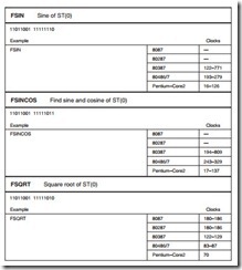
FSIN/FCOS Finds the sine or cosine of the argument located in ST expressed in radians (360° = 2π radians), with the result found in ST. The values of ST must be less than 263.

FSINCOS Finds the sine and cosine of ST, expressed in radians, and leaves the results as ST = sine and ST(1) = cosine. As with FSIN or FCOS, the initial value of ST must be less than 263.

FYL2X Finds Y log2 X. The value X is taken from the stack top, and Y is taken from ST(1). The result is found at the top of the stack after a pop. The value of X must range between 0 and ∞, and the value of Y must be between -∞ and +∞. A logarithm with any positive base (b) is found by the equation LOGb X =

(LOG2 b)-1 × LOG2 X.

FYL2P1 Finds Y log2 (X + 1). The value of X is taken from the stack top and Y is taken from ST(1). The result is found at the top of the stack after a pop. The

value of X must range between 0 and 1 –

between -∞ and +∞.

2>2 and the value of Y must be

Constant Operations

The coprocessor instruction set includes opcodes that return constants to the top of the stack. A list of these instructions appears in Table 14–7.

Coprocessor Control Instructions

The coprocessor has control instructions for initialization, exception handling, and task switching. The control instructions have two forms. For example, FINIT initializes the coprocessor, as does FNINIT. The difference is that FNINIT does not cause any wait states, while FINIT does

The Arithmetic Coprocessor, MMX,and SIMD Technologies-0269The Arithmetic Coprocessor, MMX,and SIMD Technologies-0270

cause waits. The microprocessor waits for the FINIT instruction by testing the BUSY pin on the coprocessor. All control instructions have these two forms. Following is a list of each control instruction with its function:

FINIT/FNINIT Performs a reset (initialize) operation on the arithmetic coprocessor (see Table 14–8 for the reset conditions). The coprocessor operates with a closure of projective (unsigned infinity), rounds to the nearest or even, and uses extended-precision when reset or initialized. It also sets register 0 as the top of the stack.

FSETPM Changes the addressing mode of the coprocessor to the protected- addressing mode. This mode is used when the microprocessor is also operated in the protected mode. As with the microprocessor, protected mode can only be exited by a hardware reset or, in the case of the 80386 through the Pentium 4, with a change to the control register.

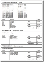
FLDCW Loads the control register with the word addressed by the operand.

FSTCW Stores the control register into the word-sized memory operand.

FSTSW AX Copies the contents of the control register to the AX register. This instruction is not available to the 8087 coprocessor.

FCLEX Clears the error flags in the status register and also the busy flag.

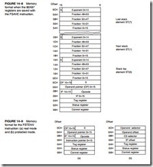
FSAVE Writes the entire state of the machine to memory. Figure 14–8 shows the memory layout for this instruction.

FRSTOR Restores the state of the machine from memory. This instruction is used to restore the information saved by FSAVE.

FSTENV Stores the environment of the coprocessor, as shown in Figure 14–9.

FLDENV Reloads the environment saved by FSTENV.

FINCSP Increments the stack pointer.

FDECSP Decrements the stack pointer.

FFREE Frees a register by changing the destination register’s tag to empty. It does not affect the contents of the register.

FNOP Floating-point coprocessor NOP.

FWAIT Causes the microprocessor to wait for the coprocessor to finish an operation. FWAIT should be used before the microprocessor accesses memory data that are affected by the coprocessor.
The Arithmetic Coprocessor, MMX,and SIMD Technologies-0271

Coprocessor Instructions

Although the microprocessor circuitry has not been discussed, the instruction sets of these coprocessors and their differences from the other versions of the coprocessor can be discussed. These newer coprocessors contain the same basic instructions provided by the earlier versions, with a few additional instructions.

The 80387, 80486, 80487SX, and Pentium through the Core2 contain the following additional instructions: FCOS (cosine), FPREM1 (partial remainder), FSIN (sine), FSINCOS (sine and

cosine), and FUCOM/FUCOMP/FUCOMPP (unordered compare). The sine and cosine instructions are the most significant addition to the instruction set. In the earlier versions of the coprocessor, the sine and cosine is calculated from the tangent. The Pentium Pro through the Core2 contain two new floating-point instructions: FCMOV (a conditional move) and FCOMI (a compare and move to flags).

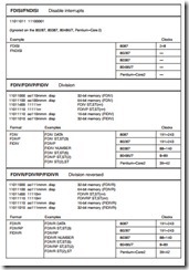
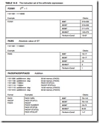
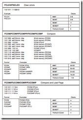
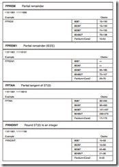
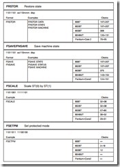
Table 14–9 lists the instruction sets for all versions of the coprocessor. It also lists the number of clocking periods required to execute each instruction. Execution times are listed for the 8087, 80287, 80387, 80486, 80487, and Core2. (The timings for the Pentium through the Pentium 4 are the same because the coprocessor is identical in each of these microprocessors.) To determine the execution time of an instruction, the clock time is multiplied times the listed execution time. The FADD instruction requires 70–143 clocks for the 80287. Suppose that an 8 MHz clock is used with the 80287. The clocking period is 1/8 MHz, or 125 ns. The FADD instruction requires between 8.75 μs and 17.875 μs to execute. Using a 33 MHz (33 ns) 80486DX2, this instruction requires between 0.264 μs and 0.66 μs to execute. On the Pentium the FADD instruction requires from 1–7 clocks, so if operated at 133 MHz (7.52 ns), the FADD requires between 0.00752 μs and 0.05264 μs. The Pentium Pro through the Core2 are even faster than the Pentium. For example, in a 3 GHz Pentium 4, which has a clock period of 0.333 ns, the FADD instruction requires between 0.333 ns and 2.333 ns to execute.

Table 14–9 uses some shorthand notations to represent the displacement that may or may not be required for an instruction that uses a memory-addressing mode. It also uses the abbrevi- ation mmm to represent a register/memory addressing mode and uses rrr to represent one of the floating-point coprocessor registers ST(0)–ST(7). The d (destination) bit that appears in some instruction opcodes defines the direction of the data flow, as in FADD ST,ST(2) or FADD ST(2),ST. The d bit is a logic 0 for flow toward ST, as in FADD ST,ST(2), where ST holds the sum after the addition; and a logic 1 for FADD ST(2),ST, where ST(2) holds the sum.

Also note that some instructions allow a choice of whether a wait is inserted. For example, the FSTSW AX instruction copies the status register into AX. The FNSTSW AX instruction also copies the status register to AX, but without a wait.
The Arithmetic Coprocessor, MMX,and SIMD Technologies-0272

The Arithmetic Coprocessor, MMX,and SIMD Technologies-0273The Arithmetic Coprocessor, MMX,and SIMD Technologies-0274The Arithmetic Coprocessor, MMX,and SIMD Technologies-0275The Arithmetic Coprocessor, MMX,and SIMD Technologies-0276The Arithmetic Coprocessor, MMX,and SIMD Technologies-0277The Arithmetic Coprocessor, MMX,and SIMD Technologies-0278The Arithmetic Coprocessor, MMX,and SIMD Technologies-0279The Arithmetic Coprocessor, MMX,and SIMD Technologies-0280The Arithmetic Coprocessor, MMX,and SIMD Technologies-0281The Arithmetic Coprocessor, MMX,and SIMD Technologies-0282The Arithmetic Coprocessor, MMX,and SIMD Technologies-0283The Arithmetic Coprocessor, MMX,and SIMD Technologies-0284The Arithmetic Coprocessor, MMX,and SIMD Technologies-0285The Arithmetic Coprocessor, MMX,and SIMD Technologies-0286


THE ARITHMETIC COPROCESSOR, MMX, AND SIMD TECHNOLOGIES:THE 80X87 ARCHITECTURE.

THE 80X87 ARCHITECTURE

The 80X87 is designed to operate concurrently with the microprocessor. Note that the 80486DX–Core2 microprocessors contain their own internal and fully compatible versions of the 80387. With other family members, the coprocessor is an external integrated circuit that parallels most of the connections on the microprocessor. The 80X87 executes 68 different instructions. The microprocessor executes all normal instructions and the 80X87 executes arithmetic coprocessor instructions. Both the microprocessor and coprocessor will execute their respective instructions simultaneously or concurrently. The numeric or arithmetic coprocessor is a special-purpose micro- processor that is especially designed to efficiently execute arithmetic and transcendental operations.

The microprocessor intercepts and executes the normal instruction set, and the coprocessor intercepts and executes only the coprocessor instructions. Recall that the coprocessor instructions are actually escape (ESC) instructions. These instructions are used by the microprocessor to generate a memory address for the coprocessor so that the coprocessor can execute a coprocessor instruction.

Internal Structure of the 80X87

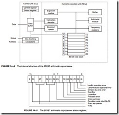
Figure 14–4 shows the internal structure of the arithmetic coprocessor. Notice that this device is divided into two major sections: the control unit and the numeric execution unit.

The control unit interfaces the coprocessor to the microprocessor-system data bus. Both the devices monitor the instruction stream. If the instruction is an ESCape (coprocessor) instruction, the coprocessor executes it; if not, the microprocessor executes it.
The numeric execution unit (NEU) is responsible for executing all coprocessor instructions. The NEU has an eight-register stack that holds operands for arithmetic instructions and the results of arithmetic instructions. Instructions either address data in specific stack data registers or use a push-and-pop mechanism to store and retrieve data on the top of the stack. Other registers in the NEU are status, control, tag, and exception pointers. A few instructions transfer data between the coprocessor and the AX register in the microprocessor. The FSTSW AX instruction is the only instruction available to the coprocessor that allows direct communications to the microprocessor through the AX register. Note that the 8087 does not contain the FSTSW AX instruction, but all newer coprocessors do contain it.
The stack within the coprocessor contains eight registers that are each 80 bits wide. These stack registers always contain an 80-bit extended-precision floating-point number. The only time that data appear as any other form is when they reside in the memory system. The coprocessor converts from signed integer, BCD, single-precision, or double-precision form as the data are moved between the memory and the coprocessor register stack.

Status Register. The status register (see Figure 14–5) reflects the overall operation of the coprocessor. The status register is accessed by executing the instruction (FSTSW), which stores the contents of the status register into a word of memory. The FSTSW AX instruction copies the status register directly into the microprocessor’s AX register on the 80187 or above coprocessor. Once status is stored in memory or the AX register, the bit positions of the

The Arithmetic Coprocessor, MMX,and SIMD Technologies-0259

status register can be examined by normal software. The coprocessor/microprocessor communications are carried out through the I/O ports 00FAH–00FFH on the 80187 and 80287, and I/O ports 800000FAH–800000FFH on the 80386 through the Pentium 4. Never use these I/O ports for interfacing I/O devices to the microprocessor.

The newer coprocessors (80187 and above) use status bit position 6 (SF) to indicate a stack overflow or underflow error. Following is a list of the status bits, except for SF, and their applications:

B The busy bit indicates that the coprocessor is busy executing a task. Busy is tested by examining the status register or by using the FWAIT instruction. Newer coprocessors automatically synchronize with the microprocessor, so the busy flag need not be tested before performing additional coprocessor tasks.

The Arithmetic Coprocessor, MMX,and SIMD Technologies-0260

C0–C3 The condition code bits indicate conditions about the coprocessor (see Table 14–2 for a complete listing of each combination of these bits and their functions). Note that these bits have different meanings for different instructions, as indicated in the table. The top of the stack is denoted as ST in this table.

TOP The top-of-stack (ST) bit indicates the current register addressed as the top-of-the- stack (ST). This is normally register ST(0).

ES The error summary bit is set if any unmasked error bit (PE, UE, OE, ZE, DE, or IE) is set. In the 8087 coprocessor, the error summary also caused a coprocessor interrupt. Since the 80187, the coprocessor interrupt has been absent from the family.

PE The precision error indicates that the result or operands exceed the selected precision.

UE An underflow error indicates a nonzero result that is too small to represent with the current precision selected by the control word.

OE An overflow error indicates a result that is too large to be represented. If this error is masked, the coprocessor generates infinity for an overflow error.

ZE A zero error indicates the divisor was zero while the dividend is a noninfinity or nonzero number.

DE A denormalized error indicates that at least one of the operands is denormalized.

IE An invalid error indicates a stack overflow or underflow, indeterminate form (0 ÷ 0, +∞, -∞, etc.), or the use of a NAN as an operand. This flag indicates errors such as those produced by taking the square root of a negative number, etc.

The Arithmetic Coprocessor, MMX,and SIMD Technologies-0261

There are two ways to test the bits of the status register once they are moved into the AX register with the FSTSW AX instruction. One method uses the TEST instruction to test individual bits of the status register. The other uses the SAHF instruction to transfer the leftmost 8 bits of the status register into the microprocessor’s flag register. Both methods are illustrated in Example 14–6. This example uses the DIV instruction to divide the top of the stack by the contents of DATA1 and the FSQRT instruction to find the square root of the top of the stack. The example also uses the FCOM instruction to compare the contents of the stack top with DATA1. Note that the conditional jump instructions are used with the SAHF instruction to test for the condition listed in Table 14–3. Although SAHF and conditional jumps cannot test all possible operating conditions of the coprocessor, they can help to reduce the complexity of certain tested conditions. Note that SAHF places C0 into the carry flag, C2 into the parity flag, and C3 into the zero flag.

If the Pentium 4 or Core2 is operated in the 64-bit mode, the SAHF instruction does not function. In the 64-bit mode, another method of testing the coprocessor flags is needed, such as testing each bit of AX for C0, C2, and C3. (See Example 14–6.)

The Arithmetic Coprocessor, MMX,and SIMD Technologies-0262The Arithmetic Coprocessor, MMX,and SIMD Technologies-0263

When the FXAM instruction and FSTSW AX are executed and followed by the SAHF instruction, the zero flag will contain C3. The FXAM instruction could be used to test a divisor before a division for a zero value by using the JZ instruction following FXAM, FSTSW AX, and SAHF.

Control Register. The control register is pictured in Figure 14–6. The control register selects the precision, rounding control, and infinity control. It also masks and unmasks the exception bits that correspond to the rightmost 6 bits of the status register. The FLDCW instruction is used to load a value into the control register.

Following is a description of each bit or grouping of bits found in the control register:

IC Infinity control selects either affine or projective infinity. Affine allows positive and negative infinity; projective assumes infinity is unsigned.

RC Rounding control determines the type of rounding, as defined in Figure 14–6. PC The precision control sets the precision of the result, as defined in Figure 14–6. Exception Determine whether the error indicated by the exception affects the error bit in masks the status register. If a logic 1 is placed in one of the exception control bits, the corresponding status register bit is masked off.

Tag Register. The tag register indicates the contents of each location in the coprocessor stack. Figure 14–7 illustrates the tag register and the status indicated by each tag. The tag indicates whether a register is valid; zero; invalid or infinity; or empty. The only way that a program can view the tag register is by storing the coprocessor environment using the FSTENV, FSAVE, or FRSTOR instructions. Each of these instructions stores the tag register along with other coprocessor data.

The Arithmetic Coprocessor, MMX,and SIMD Technologies-0264


THE ARITHMETIC COPROCESSOR, MMX, AND SIMD TECHNOLOGIES:THE ARITHMETIC COPROCESSOR, MMX, AND SIMD TECHNOLOGIES.

THE ARITHMETIC COPROCESSOR, MMX, AND SIMD TECHNOLOGIES

INTRODUCTION

The Intel family of arithmetic coprocessors includes the 8087, 80287, 80387SX, 80387DX, and the 80487SX for use with the 80486SX microprocessor. The 80486DX–Core2 microprocessors contain their own built-in arithmetic coprocessors. Be aware that some of the cloned 80486 microprocessors (from IBM and Cyrix) did not contain arithmetic coprocessors. The instruction sets and programming for all devices are almost identical; the main difference is that each coprocessor is designed to function with a different Intel microprocessor. This chapter provides detail on the entire family of arithmetic coprocessors. Because the coprocessor is a part of the 80486DX–Core2, and because these microprocessors are commonplace, many programs now require or at least benefit from a coprocessor.

The family of coprocessors, which is labeled the 80X87, is able to multiply, divide, add, subtract, find the square root, and calculate the partial tangent, partial arctangent, and logarithms. Data types include 16-, 32-, and 64-bit signed integers; l8-digit BCD data; and 32-, 64-, and 80-bit floating-point numbers. The operations performed by the 80X87 generally execute many times faster than equivalent operations written with the most efficient programs that use the microprocessor’s normal instruction set. With the improved Pentium coprocessor, operations execute about five times faster than those performed by the 80486 microprocessor with an equal clock frequency. Note that the Pentium can often execute a coprocessor instruction and two integer instructions simultaneously. The Pentium Pro through Core2 coprocessors are similar in performance to the Pentium coprocessor, except that a few new instructions have been added: FCMOV and FCOMI.

The multimedia extensions (MMX) to the Pentium–Core2 are instructions that share the arithmetic coprocessor register set. The MMX extension is a special internal processor designed to execute integer instructions at high-speed for external multimedia devices. For this reason, the MMX instruction set and specifications have been placed in this chapter. The SIMD (single- instruction, multiple data) extensions, which are called SSE (streaming SIMD extensions), are similar to the MMX instructions, but function with floating-point numbers instead of integers and do not use the coprocessor register space as do MMX instructions.

CHAPTER OBJECTIVES

Upon completion of this chapter, you will be able to:

1. Convert between decimal data and signed integer, BCD, and floating-point data for use by the arithmetic coprocessor, MMX, and SIMD technologies.

2. Explain the operation of the 80X87 arithmetic coprocessor and the MMX and SIMD units.

3. Explain the operation and addressing modes of each arithmetic coprocessor, MMX, and SSE instruction.

4. Develop programs that solve complex arithmetic problems using the arithmetic coprocessor, MMX, and SIMD instructions.

DATA FORMATS FOR THE ARITHMETIC COPROCESSOR

This section of the text presents the types of data used with all arithmetic coprocessor family members. (See Table 14–1 for a listing of all Intel microprocessors and their companion coprocessors.) These data types include signed integer, BCD, and floating-point. Each has a specific use in a system, and many systems require all three data types. Note that assembly language programming with the coprocessor is often limited to modifying the coding generated by a high- level language such as C/C++. In order to accomplish any such modification, the instruction set and some basic programming concepts are required, which are presented in this chapter.

Signed Integers

The signed integers used with the coprocessor are the same as those described in Chapter 1. When used with the arithmetic coprocessor, signed integers are 16- (word), 32- (doubleword integer), or 64-bits (quadword integer) wide. The long integer is new to the coprocessor and is not described in Chapter 1, but the principles are the same. Conversion between decimal and signed integer format is handled in exactly the same manner as for the signed integers described in Chapter 1. As you will recall, positive numbers are stored in true form with a leftmost sign-bit of 0, and negative numbers are stored in two’s complement form with a leftmost sign-bit of 1.

The word integers range in value from -32,768 to +32,767, the doubleword integer range is ±2 ×10⁹, and the quadword integer range is ±9 × 10¹⁸. Integer data types are found in some applications that use the arithmetic coprocessor. See Figure 14–1, which shows these three forms of signed integer data.

Data are stored in memory using the same assembler directives described and used in earlier chapters. The DW directive defines words, DD defines doubleword integers, and DQ defines quadword integers. Example 14–1 shows how several different sizes of signed integers are defined for use by the assembler and arithmetic coprocessor.

The Arithmetic Coprocessor, MMX,and SIMD Technologies-0251The Arithmetic Coprocessor, MMX,and SIMD Technologies-0252

Binary-Coded Decimal (BCD)

The binary-coded decimal (BCD) form requires 80 bits of memory. Each number is stored as an 18-digit packed integer in nine bytes of memory as two digits per byte. The tenth byte contains only a sign-bit for the 18-digit signed BCD number. Figure 14–2 shows the format of the BCD number used with the arithmetic coprocessor. Note that both positive and negative numbers are stored in true form and never in ten’s complement form. The DT directive stores BCD data in the memory as illustrated in Example 14–2. This form is rarely used because it is unique to the Intel coprocessor.

The Arithmetic Coprocessor, MMX,and SIMD Technologies-0253

Floating-Point

Floating-point numbers are often called real numbers because they hold signed integers, fractions, and mixed numbers. A floating-point number has three parts: a sign-bit, a biased exponent, and a significand. Floating-point numbers are written in scientific binary notation. The Intel family of arithmetic coprocessors supports three types of floating-point numbers: single (32 bits), double (64 bits), and temporary (80 bits). See Figure 14–3 for the three forms of the floating-point number. Please note that the single form is also called a single-precision number and the double form is called a double-precision number. Sometimes the 80-bit temporary form is called an extended-precision number. The floating-point numbers and the operations performed by the arithmetic coprocessor conform to the IEEE-754 standard, as adopted by all major personal computer software producers. This includes Microsoft, which in 1995 stopped supporting the Microsoft floating-point format and also the ANSI floating-point standard that is popular in some mainframe computer systems.

The Arithmetic Coprocessor, MMX,and SIMD Technologies-0254The Arithmetic Coprocessor, MMX,and SIMD Technologies-0255

In Visual C++ 2008 or the Express edition, float, double, and decimal are used for the three data types. The float is a 32-bit version, double is the 64-bit version, and decimal is a special version developed for Visual studio that develops a very accurate floating-point number for use in banking transactions or anything else that requires a high degree of precision. The decimal variable form is new to Visual Studio 2005 and 2008.

Converting to Floating-Point Form. Converting from decimal to the floating-point form is a simple task that is accomplished through the following steps:

1. Convert the decimal number to binary.

2. Normalize the binary number.

3. Calculate the biased exponent.

4. Store the number in the floating-point format.

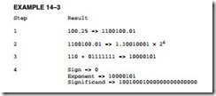
These four steps are illustrated for the decimal number 100.2510 in Example 14–3. Here, the decimal number is converted to a single-precision (32-bit) floating-point number.

The Arithmetic Coprocessor, MMX,and SIMD Technologies-0256

In step 3 of Example 14–3, the biased exponent is the exponent, a 26 or 110, plus a bias of 01111111 (7FH) or 10000101 (85H). All single-precision numbers use a bias of 7FH, double- precision numbers use a bias of 3FFH, and extended-precision numbers use a bias of 3FFFH.

In step 4 of Example 14–3, the information found in the prior steps is combined to form the floating-point number. The leftmost bit is the sign-bit of the number. In this case, it is a 0 because the number is +100.2510. The biased exponent follows the sign-bit. The significand is a 23-bit number with an implied one-bit. Note that the significand of a number l.XXXX is the XXXX portion. The 1. is an implied one-bit that is only stored in the extended temporary-precision form of the floating-point number as an explicit one-bit.

Some special rules apply to a few numbers. The number 0, for example, is stored as all zeros except for the sign-bit, which can be a logic 1 to represent a negative zero. The plus and minus infinity is stored as logic 1s in the exponent with a significand of all zeros and the sign-bit that represents plus or minus. A NAN (not-a-number) is an invalid floating-point result that has all ones in the exponent with a significand that is not all zeros.

Converting from Floating-Point Form. Conversion to a decimal number from a floating-point number is summarized in the following steps:

1. Separate the sign-bit, biased exponent, and significand.

2. Convert the biased exponent into a true exponent by subtracting the bias.

3. Write the number as a normalized binary number.

4. Convert it to a denormalized binary number.

5. Convert the denormalized binary number to decimal.

These five steps convert a single-precision floating-point number to decimal, as shown in Example 14–4. Notice how the sign-bit of 1 makes the decimal result negative. Also notice that the implied one-bit is added to the normalized binary result in step 3.

The Arithmetic Coprocessor, MMX,and SIMD Technologies-0257

Storing Floating-Point Data in Memory. Floating-point numbers are stored with the assembler using the DD directive for single-precision, DQ for double-precision, and DT for extended temporary-precision. Some examples of floating-point data storage are shown in Example 14–5. The author discovered that the Microsoft macro assembler contains an error that does not allow a plus sign to be used with positive floating-point numbers. A +92.45 must be defined as 92.45 for the assembler to function correctly. Microsoft has assured the author that this error has been corrected in version 6.11 of MASM if the REAL4, REAL8, or REAL10 directives are used in place of DD, DQ, and DT to specify floating-point data. The assembler provides access 8087 emulator if your system does not contain a microprocessor with a coprocessor. The emulator comes with all Microsoft high-level languages or as shareware programs such as EM87. Access the emulator by including the OPTION EMULATOR statement immediately following the .MODEL statement in a program. Be aware that the emulator does not emulate some of the coprocessor instructions. Do not use this option if your system contains a coprocessor. In all cases, you must include the .8087, .80187, .80287, .80387, .80487, .80587, or .80687 switch to enable the generation of coprocessor instructions.

The Arithmetic Coprocessor, MMX,and SIMD Technologies-0258


DIRECT MEMORY ACCESS AND DMA-CONTROLLED I/O:VIDEO DISPLAYS.

VIDEO DISPLAYS

Modern video displays are OEM (original equipment manufacturer) devices that are usually purchased and incorporated into a system. Today, there are many different types of video displays available in either color or monochrome versions.

Monochrome versions usually display information using amber, green, or paper-white dis- plays. The paper-white displays were once extremely popular for many applications. The most common of these applications are desktop publishing and computer-aided drafting (CAD).

The color displays are more diverse and have all but replaced the black-and-white display. Color display systems are available that accept information as a composite video signal, much like your home television, as TIL voltage level signals (0 or 5 V), and as analog signals (0–0.7 V). Composite video displays are disappearing because the available resolution is too low. Today, many applications require high-resolution graphics that cannot be displayed on a composite dis- play such as a home television receiver. Early composite video displays were found with Commodore 64, Apple 2, and similar computer systems.

Video Signals

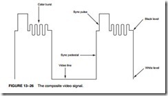
Figure 13–26 illustrates the signal sent to a composite video display. This signal is composed of several parts that are required for this type of display. The signals illustrated represent the signals sent to a color composite-video monitor. Notice that these signals include not only video, but also include sync pulses, sync pedestals, and a color burst. Notice that no audio signal is illustrated because one

Direct Memory Access and DMA-Controlled I-O-0244

often does not exist. Rather than include audio with the composite video signal, audio is developed in the computer and output from a speaker inside the computer cabinet. It can also be developed by a sound system and output in stereo to external speakers. The major disadvantages of the composite video display are the resolution and color limitations. Composite video signals were designed to emulate television video signals so that a home television receiver could function as a video monitor.

Most modern video systems use direct video signals that are generated with separate sync signals. In a direct video system, video information is passed to the monitor through a cable that uses separate lines for video and also synchronization pulses. Recall that these signals were combined in a composite video signal.

A monochrome (one color) monitor uses one wire for video, one for horizontal sync, and one for vertical sync. Often, these are the only signal wires found. A color video monitor uses three video signals. One signal represents red, another green, and the third blue. These monitors are often called RGB monitors for the video primary colors of light: red (R), green (G), and blue (B).

The TTL RGB Monitor

The RGB monitor is available as either an analog or TTL monitor. The RGB monitor uses TTL level signals (0 or 5 V) as video inputs and a fourth line called intensity to allow a change in intensity. The RGB video TTL display can display a total of 16 different colors. The TTL RGB monitor is used in the CGA (color graphics adapter) system found in older computer systems.

Table 13–4 lists these 16 colors and also the TTL signals present to generate them. Eight of the 16 colors are generated at high intensity and the other eight at low intensity. The three video colors are red, green, and blue. These are primary colors of light. The secondary colors are cyan, magenta, and yellow. Cyan is a combination of blue and green video signals, and is blue-green in color. Magenta is a combination of blue and red video signals, and is a purple color.

Yellow (high intensity) and brown (low intensity) are both a combination of red and green video signals. If additional colors are desired, TTL video is not normally used. A scheme was developed by using low- and medium-color TTL video signals, which provided 32 colors, but it proved to have little application and never found widespread use in the field.

Figure 13–27 illustrates the connector most often found on the TTL RGB monitor or a TTL monochrome monitor. The connector illustrated is a 9-pin connector. Two of the connections are used for ground, three for video, two for synchronization or retrace signals, and one for

Direct Memory Access and DMA-Controlled I-O-0245

intensity. Notice that pin 7 is labeled normal video. This is the pin used on a monochrome monitor for the luminance or brightness signal. Monochrome TTL monitors use the same 9-pin con- nector as RGB TTL monitors.

The Analog RGB Monitor

In order to display more than 16 colors, an analog video display is required. These are often called analog RGB monitors. Analog RGB monitors still have three video input signals, but don’t have the intensity input. Because the video signals are analog signals instead of two-level TTL signals, they are at any voltage level between 0.0 V and 0.7 V, which allows an infinite number of colors to be displayed. This is because an infinite number of voltage levels between the minimum and maximum could be generated. In practice, a finite number of levels are generated. This is usually either 256K, 16M, or 24M colors, depending on the standard.

Figure 13–28 illustrates the connector used for an analog RGB or analog monochrome monitor. Notice that the connector has 15 pins and supports both RGB and monochrome analog displays. The way data are displayed on an analog RGB monitor depends upon the interface standard used with the monitor. Pin 9 is a key, which means that no hole exists on the female connector for this pin.

Another type of connector for the analog RGB monitor that is becoming common is called the DVI-D (digital visual interface) connector. The -D is for digital and is the most common interface of

Direct Memory Access and DMA-Controlled I-O-0246Direct Memory Access and DMA-Controlled I-O-0247

this type. Figure 13–29 illustrates the female connector found on newer monitors and video cards. Also found on television and video equipment is the HDMI (high-definition multimedia interface) connector. This has not made its way to digital video cards, but will probably appear in the future. Eventually all video equipment will use the HDMI connector for its connection.

Most analog displays use a digital-to-analog converter (DAC) to generate each color video voltage. A common standard uses a 8-bit DAC for each video signal to generate 256 different voltage levels between 0 V and 0.7 V. There are 256 different red video levels, 256 different green video levels, and 256 different blue video levels. This allows 256 × 256 × 256, or 16,777,216 (16 M) colors to be displayed.

Figure 13–30 illustrates the video generation circuit employed in many common video standards such as the short-lived EGA (enhanced graphics adapter) and VGA (variable graphics array), as used with an IBM PC. This circuit is used to generate VGA video. Notice that each color is generated with an 18-bit digital code. Six of the 18 bits are used to generate each video color voltage when applied to the inputs of a 6-bit DAC.

Direct Memory Access and DMA-Controlled I-O-0248Direct Memory Access and DMA-Controlled I-O-0249

A high-speed palette SRAM (access time of less than 40 ns) is used to store 256 different 18-bit codes that represent 256 different hues. This 18-bit code is applied to the digital-to-analog converters. The address input to the SRAM selects one of the 256 colors stored as 18-bit binary codes. This system allows 256 colors out of a possible 256K colors to be displayed at one time. In order to select any of 256 colors, an 8-bit code that is stored in the computer’s video display RAM is used to specify the color of a picture element. If more colors are used in a system, the code must be wider. For example, a system that displays 1024 colors out of 256K colors requires a 10-bit code to address the SRAM that contains 1024 locations, each containing an 18-bit color code. Some newer systems use a larger palette SRAM to store up to 64K of different color codes.

Whenever a color is placed on the video display, provided that RTC is a logic 0, the system sends the 8-bit code that represents a color to the D0 –D7 connections. The PLD then generates a clock pulse for U10, which latches the color code. After 40 ns (one 25 MHz clock), the PLD generates a clock pulse for the DAC latches (U7, U8, and U9). This amount of time is required for the palette SRAM to look up the 18-bit contents of the memory location selected by U10. Once the color code (18-bit) is latched into U7–U9, the three DACs convert it to three video voltages for the monitor. This process is repeated for each 40-ns-wide picture element (pixel) that is displayed. The pixel is 40 ns wide because a 25 MHz clock is used in this system. Higher resolution is attainable if a higher clock frequency is used with the system.

If the color codes (18-bits) stored in the SRAM must be changed, this is always accomplished during retrace when RTC is a logic 1. This prevents any video noise from disrupting the image displayed on the monitor.

In order to change a color, the system uses the S0, S1, and S2 inputs of the PLD to select U1, U2, U3, and U10. First, the address of the color to be changed is sent to latch U10, which addresses a location in the palette SRAM. Next, each new video color is loaded into U1, U2, and U3. Finally, the PLD generates a write pulse for the WE input to the SRAM to write the new color code into the palette SRAM.

Retrace occurs 70.1 times per second in the vertical direction and 31,500 times per second in the horizontal direction for a 640 × 480 display. During retrace, the video signal voltage sent to the display must be 0 V, which causes black to be displayed during the retrace. Retrace itself is used to move the electron beam to the upper left-hand corner for vertical retrace and to the left margin of the screen for horizontal retrace.

The circuit illustrated causes U4 – U6 buffers to be enabled so that they apply 000000 each to the DAC latch for retrace. The DAC latches capture this code and generate 0 V for each video color signal to blank the screen. By definition, 0 V is considered to be the black level for video and 0.7 V is considered to be the full intensity on a video color signal.

The resolution of the display, for example, 640 × 480, determines the amount of memory required for the video interface card. If this resolution is used with a 256-color display (8 bits per pixel), then 640 × 480 bytes of memory (307,200) are required to store all of the pixels for the display. Higher resolution displays are possible, but, as you can imagine, even more memory is required. A 640 × 480 display has 480 video raster lines and 640 pixels per line. A raster line is the horizontal line of video information that is displayed on the monitor. A pixel is the smallest subdivision of this horizontal line.

Figure 13–31 illustrates the video display, showing the video lines and retrace. The slant of each video line in this illustration is greatly exaggerated, as is the spacing between lines. This illustration shows retrace in both the vertical and horizontal directions. In the case of a VGA dis- play, as described, the vertical retrace occurs exactly 70.1 times per second and the horizontal retrace occurs exactly 31,500 times per second.

In order to generate 640 pixels across one line, it takes 40 ns × 640, or 25.6 μs. A horizontal time of 31,500 Hz allows a horizontal line time of 1/31,500, or 31.746 μs. The difference between these two times is the retrace time allowed to the monitor. (The Apple Macintosh has a horizontal line time of 28.57 μs.)

Because the vertical retrace repetition rate is 70.1 Hz, the number of lines generated is determined by dividing the vertical time into the horizontal time. In the case of a VGA display (a 640 × 400 display), this is 449.358 lines. Only 400 of these lines are used to display information; the rest are lost during the retrace. Because 49.358 lines are lost during the retrace, the retrace time is 49.358 × 31.766 μs, or 1568 μs. It is during this relatively large amount of time that the color palette SRAM is changed or the display memory system is updated for a new video display.

Direct Memory Access and DMA-Controlled I-O-0250

In the Apple Macintosh computer (640 × 480), the number of lines generated is 525 lines. Of the total number of lines, 45 are lost during vertical retrace.

Other display resolutions are 800 × 600 and 1024 × 768. The 800 × 600 SVGA (super VGA) display is ideal for a 14" color monitor, while the 1024 × 768 EVGA or XVGA (extended VGA) is ideal for a 21" or 25" monitor used in CAD systems. These resolutions sound like just another set of numbers, but realize that an average home television receiver has a resolution approximately 400 × 300. The high-resolution display available on computer systems is much clearer than that available as home television. A resolution of 1024 × 768 approaches that found in 35 mm film. The only dis- advantage of the video display on a computer screen is the number of colors displayed at a time, but as time passes, this will surely improve. Additional colors allow the image to appear more realistically because of subtle shadings that are required for a true high-quality, lifelike image.

If a display system operates with a 60 Hz vertical time and a 15,600 Hz horizontal time, the number of lines generated is 15,600/60, or 260 lines. The number of usable lines in this system is most likely 240, where 20 are lost during vertical retrace. It is clear that the number of scanning lines is adjustable by changing the vertical and horizontal scanning rates. The vertical scanning rate must be greater than or equal to 50 Hz or flickering will occur. The vertical rate must not be higher than about 75 Hz or problems with the vertical deflection coil may occur. The electron beam in a monitor is positioned by an electrical magnetic field generated by coils in a yoke that surrounds the neck of the picture tube. Because the magnetic field is generated by coils, the frequency of the signal applied to the coil is limited.

The horizontal scanning rate is also limited by the physical design of the coils in the yoke. Because of this, it is normal to find the frequency applied to the horizontal coils within a narrow range. This is usually 30,000 Hz–37,000 Hz or 15,000 Hz–17,000 Hz. Some newer monitors are called multisync monitors because the deflection coil is taped so that it can be driven with differ- ent deflection frequencies. Sometimes, both the vertical and horizontal coils are both taped for different vertical and horizontal scanning rates.

High-resolution displays use either interlaced or noninterlaced scanning. The non- interlaced scanning system is used in all standards except the highest. In the interlaced system, the video image is displayed by drawing half the image first with all of the odd scanning lines, then the other half is drawn using the even scanning lines. Obviously, this system is more complex and is only more efficient because the scanning frequencies are reduced by 50% in an interlaced system. For example, a video system that uses 60 Hz for the vertical scanning frequency and 15,720 Hz for the horizontal frequency generates 262 (15,720/60) lines of video at the rate of 60 full frames per second. If the horizontal frequency is changed slightly to 15,750 Hz, 262.5 (15,750/60) lines are generated, so two full sweeps are required to draw one complete picture of 525 video lines. Notice how just a slight change in horizontal frequency doubled the number of raster lines.


QUESTIONS AND PROBLEMS ON DIRECT MEMORY ACCESS AND DMA-CONTROLLED I/O.

QUESTIONS AND PROBLEMS

1. Which microprocessor pins are used to request and acknowledge a DMA transfer?

2. Explain what happens whenever a logic 1 is placed on the HOLD input pin.

3. A DMA read transfers data from to .

4. A DMA write transfers data from to .

5. The DMA controller selects the memory location used for a DMA transfer through what bus signals?

6. The DMA controller selects the I/O device used during a DMA transfer by which pin?

7. What is a memory-to-memory DMA transfer?

8. Describe the effect on the microprocessor and DMA controller when the HOLD and HLDA pins are at their logic 1 levels.

9. Describe the effect on the microprocessor and DMA controller when the HOLD and HLDA pins are at their logic 0 levels.

10. The 8237 DMA controller is a(n) channel DMA controller.

11. If the 8237 DMA controller is decoded at I/O ports 2000H –200FH, what ports are used to program channel 1?

12. Which 8237 DMA controller register is programmed to initialize the controller?

13. How many bytes can be transferred by the 8237 DMA controller?

14. Write a sequence of instructions that transfer data from memory location 21000H –210FFH to 20000H –200FFH by using channel 2 of the 8237 DMA controller. You must initialize the 8237 and use the latch described in Section 12–1 to hold A19 –A16.

15. Write a sequence of instructions that transfers data from memory to an external I/O device by

using Channel 3 of the 8237. The memory area to be transferred is at location 20000H – 20FFFH.

16. What is a pen drive?

17. The 3 1/2" disk is known as a(n) floppy disk.

18. Data are recorded in concentric rings on the surface of a disk known as a(n) .

19. A track is divided into sections of data called .

20. On a double-sided disk, the upper and lower tracks together are called a(n) .

21. Why is NRZ recording used on a disk memory system?

22. Draw the timing diagram generated to write a 1001010000 using MFM encoding.

23. Draw the timing diagram generated to write a 1001010000 using RLL encoding.

24. What is a flying head?

25. Why must the heads on a hard disk be parked?

26. What is the difference between a voice coil head position mechanism and a stepper motor head positioning mechanism?

27. What is a WORM?

28. What is a CD-ROM?

29. How much data can be stored on a common DVD, an HD-DVD, and a Blu-ray DVD?

30. What is the difference between a TTL monitor and an analog monitor?

31. What are the three primary colors of light?

32. What are the three secondary colors of light?

33. What is a pixel?

34. A video display with a resolution of 1280 × 1024 contains lines, with each line divided into pixels.

35. Explain how a TTL RGB monitor can display 16 different colors.

36. What are the DVI-D and HDMI connectors?

37. Explain how an analog RGB monitor can display an infinite number of colors.

38. If an analog RGB video system uses 8-bit DACs, it can generate different colors.

39. If a video system uses a vertical frequency of 60 Hz and a horizontal frequency of 32,400 Hz, how many raster lines are generated?


SUMMARY OF DIRECT MEMORY ACCESS AND DMA-CONTROLLED I/O.

SUMMARY

1. The HOLD input is used to request a DMA action, and the HLDA output signals that the hold is in effect. When a logic 1 is placed on the HOLD input, the microprocessor (1) stops executing the program; (2) places its address, data, and control bus at their high-impedance state; and (3) signals that the hold is in effect by placing a logic 1 on the HLDA pin.

2. A DMA read operation transfers data from a memory location to an external I/O device. A DMA write operation transfers data from an I/O device into the memory. Also available is a memory-to-memory transfer that allows data to be transferred between two memory locations by using DMA techniques.

3. The 8237 direct memory access (DMA) controller is a four-channel device that can be expanded to include an additional channel of DMA.

4. Disk memory comes in the form of floppy disk storage that is found as 31⁄2" micro-floppy

disks. Disks are found as double-sided, double-density (DSDD), or as high-density (HD) storage devices. The DSDD 31⁄2" disk stores 720K bytes of data and the HD 31⁄2" disk stores 1.44M bytes of data.

5. Floppy disk memory data are stored using NRZ (non-return to zero) recording. This method saturates the disk with one polarity of magnetic energy for a logic 1 and the opposite polarity for a logic 0. In either case, the magnetic field never returns to 0. This technique eliminates the need for a separate erase head.

6. Data are recorded on disks by using either modified frequency modulation (MFM) or run- length limited (RLL) encoding schemes. The MFM scheme records a data pulse for a logic 1, no data or clock for the first logic 0 of a string of zeros, and a clock pulse for the second and subsequent logic 0 in a string of zeros. The RLL scheme encodes data so that 50% more information can be packed onto the same disk area. Most modern disk memory systems use the RLL encoding scheme.

7. Video monitors are either TTL or analog. The TTL monitor uses two discrete voltage levels of 0 V and 5.0 V. The analog monitor uses an infinite number of voltage levels between 0.0 V and 0.7 V. The analog monitor can display an infinite number of video levels, while the TTL monitor is limited to two video levels.

8. The color TTL monitor displays 16 different colors. This is accomplished through three video signals (red, green, and blue) and an intensity input. The analog color monitor can display an infinite number of colors through its three video inputs. In practice, the most common form of color analog display system (VGA) can display 16 M different colors.

9. The video standards found today include VGA (640 × 480), SVGA (800 × 600), and EVGA or XVGA (1024 × 768). In all three cases, the video information can be 16M colors.


DIRECT MEMORY ACCESS AND DMA-CONTROLLED I/O:DISK MEMORY SYSTEMS.

DISK MEMORY SYSTEMS

Disk memory is used to store long-term data. Many types of disk storage systems are available today and they use magnetic media, except the optical disk memory that stores data on a plastic disk. Optical disk memory is either a CD-ROM (compact disk/read only memory) that is read, but never written, or a WORM (write once/read mostly) that is read most of the time, but can be written once by a laser beam. Also becoming available is optical disk memory that can be read and written many times, but there is still a limitation on the number of write operations allowed. The latest optical disk technology is called DVD (digital-versatile disk). The DVD (8.5G) is also available in high-resolution versions for video and data storage as Blray (50G) or HD-DVD (30G). This section of the chapter provides an introduction to disk memory systems so that they may be used with computer systems. It also provides details of their operation.

Floppy Disk Memory

Once the most common and the most basic form of disk memory was the floppy, or flexible disk. Today the floppy is beginning to vanish and may completely disappear shortly in favor of the USB pen drive. The floppy disk magnetic recording media have been made available in three sizes: the 8" standard, 51/4" mini-floppy, and the 31/2" micro-floppy. Today, the 8" standard version and 51/4" mini-floppy have all but disappeared, giving way to the micro-floppy disks and more recently pen drives. The 8" disk is too large and difficult to handle and stockpile. To solve this problem, industry developed the 51/4" mini-floppy disk. Today, the micro-floppy disk has just about replaced the mini-floppy in newer systems because of its reduced size, ease of storage, and durability. Even so, systems are still marketed with the micro-floppy disk drives.

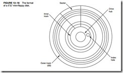
All disks and even the pen drives have several things in common. They are all organized so that data are stored in tracks. A track is a concentric ring of data that is stored on a surface of a disk. Figure 13–18 illustrates the surface of a 51/4" mini-floppy disk, showing a track that is divided into sectors. A sector is a common subdivision of a track that is designed to hold a reasonable amount of data. In many systems, a sector holds either 512 or 1024 bytes of data. The size of a sector can vary from 128 bytes to the length of one entire track.

Notice in Figure 13–18 that there is a hole through the disk that is labeled an index hole. The index hole is designed so that the electronic system that reads the disk can find the beginning of a track and its first sector (00). Tracks are numbered from track 00, the outermost track, in increasing value toward the center or innermost track. Sectors are often numbered from sector 00 on the outermost track to whatever value is required to reach the innermost track and its last sector.

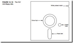
The 5 1/4" Mini-floppy Disk. Today, the 51/4" floppy is very difficult to find and is used only with older microcomputer systems. Figure 13–19 illustrates this mini-floppy disk. The floppy disk is rotated at 300 RPM inside its semi-rigid plastic jacket. The head mechanism in a floppy disk drive makes physical contact with the surface of the disk, which eventually causes wear and damage to the disk.

Most mini-floppy disks are double-sided. This means that data are written on both the top and bottom surfaces of the disk. A set of tracks called a cylinder consists of one top and one bottom track. Cylinder 00, for example, consists of the outermost top and bottom tracks.

Floppy disk data are stored in the double-density format, which uses a recording technique called MFM (modified frequency modulation) to store the information. Double-density, double-sided (DSDD) disks are normally organized with 40 tracks of data on each side of the

Direct Memory Access and DMA-Controlled I-O-0235Direct Memory Access and DMA-Controlled I-O-0236

disk. A double-density disk track is typically divided into nine sectors, with each sector containing 512 bytes of information. This means that the total capacity of a double-density, double-sided disk is 40 tracks per side × 2 sides × 9 sectors per track × 512 bytes per sector, or 368,640 (360K) bytes of information.

Also common are high-density (HD) mini-floppy disks. A high-density mini-floppy disk contains 80 tracks of information per side, with eight sectors per track. Each sector contains 1024 bytes of information. This gives the 51/4" high-density, mini-floppy disk a total capacity of 80 tracks per side × 2 sides × 15 sectors per track × 512 bytes per sector, or 1,228,800 (approximately 1.2 M) bytes of information.

The magnetic recording technique used to store data on the surface of the disk is called non-return to zero (NRZ) recording. With NRZ recording, magnetic flux placed on the surface of the disk never returns to zero. Figure 13–20 illustrates the information stored in a portion of a track. It also shows how the magnetic field encodes the data. Note that arrows are used in this illustration to show the polarity of the magnetic field stored on the surface of the disk.

The main reason that this form of magnetic encoding was chosen is that it automatically erases old information when new information is recorded. If another technique were used, a separate erase head would be required. The mechanical alignment of a separate erase head and a

Direct Memory Access and DMA-Controlled I-O-0237Direct Memory Access and DMA-Controlled I-O-0238

separate read/write head is virtually impossible. The magnetic flux density of the NRZ signal is so intense that it completely saturates (magnetizes) the surface of the disk, erasing all prior data. It also ensures that information will not be affected by noise because the amplitude of the magnetic field contains no information. The information is stored in the placement of the changes of the magnetic field.

Data are stored in the form of MFM (modified frequency modulation) in modern floppy disk systems. The MFM recording technique stores data in the form illustrated in Figure 13–21. Notice that each bit time is 2.0 μs wide on a double-density disk. This means that data are recorded at the rate of 500,000 bits per second. Each 2.0 μs bit time is divided into two parts: One part is designated to hold a clock pulse and the other holds a data pulse. If a clock pulse is pre- sent, it is 1.0 μs wide, as is a data pulse. Clock and data pulses are never present at the same time in one bit period. (Note that high-density disk drives halve these times so that a bit time is 1.0 μs and a clock or data pulse is 0.5 μs wide. This also doubles the transfer rate to 1 million bits per second [1 Mbps]).

If a data pulse is present, the bit time represents a logic 1. If no data or no clock is present, the bit time represents a logic 0. If a clock pulse is present with no data pulse, the bit time also represents a logic 0. The rules followed when data are stored using MFM are as follows:

1. A data pulse is always stored for a logic l.

2. No data and no clock are stored for the first logic 0 in a string of logic 0s.

3. The second and subsequent logic 0s in a row contain a clock pulse, but no data pulse.

The reason that a clock is inserted as the second and subsequent zero in a row is to maintain synchronization as data are read from the disk. The electronics used to recapture the data from the disk drive use a phase-locked loop to generate a clock and a data window. The phase- locked loop needs a clock or data to maintain synchronized operation.

The 3 1/2 " Micro-Floppy Disk. A popular disk size is the 31/2" micro-floppy disk. Recently, this size floppy disk has begun to be replaced by the USB pen drive as the dominant transportable media. The micro-floppy disk is a much improved version of the mini-floppy disk described earlier. Figure 13–22 illustrates the 31/2" micro-floppy disk.

Disk designers noticed several shortcomings of the mini-floppy, which is a scaled down version of the 8" standard floppy, soon after it was released. Probably one of the biggest problems with the mini-floppy is that it is packaged in a semi-rigid plastic cover that bends easily. The micro-floppy is packaged in a rigid plastic jacket that will not bend easily. This provides a much greater degree of protection to the disk inside the jacket.

Another problem with the mini-floppy is the head slot that continually exposes the surface of the disk to contaminants. This problem is also corrected on the micro-floppy because it is constructed with a spring-loaded sliding head door. The head door remains closed until the disk is inserted into the drive. Once inside the drive, the drive mechanism slides open the door, exposing the surface of the disk to the read/write heads. This provides a great deal of protection to the surface of the micro-floppy disk.

Direct Memory Access and DMA-Controlled I-O-0239

Yet another improvement is the sliding plastic write-protection mechanism on the micro- floppy disk. On the mini-floppy disk, a piece of tape was placed over a notch on the side of the jacket to prevent writing. This plastic tape easily became dislodged inside disk drives, causing problems. On the micro-floppy, an integrated plastic slide has replaced the tape write-protection mechanism. To write-protect (prevent writing) the micro-floppy disk, the plastic slide is moved to open the hole through the disk jacket. This allows light to strike a sensor that inhibits writing.

Still another improvement is the replacement of the index hole with a different drive mechanism. The drive mechanism on the mini-floppy allows the disk drive to grab the disk at any point. This requires an index hole so that the electronics can find the beginning of a track. The index hole is another trouble spot because it collects dirt and dust. The micro-floppy has a drive mechanism that is keyed so that it only fits one way inside the disk drive. The index hole is no longer required because of this keyed drive mechanism. Because of the sliding head mechanism and the fact that no index hole exists, the micro-floppy disk has no place to catch dust or dirt.

Two types of micro-floppy disks are widely available: the double-sided, double-density (DSDD) and the high-density (HD). The double-sided, double-density micro-floppy disk has 80 tracks per side, with each track containing nine sectors. Each sector contains 512 bytes of information. This allows 80 tracks per side × 2 sides × 9 sectors × 512 bytes per sector, or 737,280 (720K) bytes of data to be stored on a double-density, double-sided floppy disk.

The high-density, double-sided micro-floppy disk stores even more information. The high- density version has 80 tracks per side, but the number of sectors is doubled to 18 per track. This format still uses 512 bytes per sector, as did the double-density format. The total number of bytes on a high-density, double-sided micro-floppy disk is 80 tracks per side × 2 sides × 18 sectors per track × 512 bytes per sector, or 1,474,560 (1.44M) bytes of information.

Pen Drives

Pen drives, or flash drives, as they are often called, are replacements for floppy disk drives that use flash memory to store data. A driver, which is part of Windows (except for Windows 98), treats the pen drive as a floppy with tracks and sectors even though it really does not contain tracks and sectors. As with a floppy, the FAT system is used for the file structure. The memory in this type of drive is serial memory. When a pen drive is connected to the USB bus, the operating system recognizes it and allows data to be transferred between it and the computer.

Newer pen drives use the USB 2.0 bus specification to transfer data at a much higher rate of speed than the older USB 1.1 specification. Transfer speeds for USB 1.1 are a read speed of 750 KBps and a write speed of 450 KBps. The USB 2.0 pen drives have a transfer speed of about 48 MBps. The pen drive is currently available in sizes up to 4G bytes and has an erase cycle of up to 1,000,000 erases. The price is very reasonable when compared to the floppy disk.

Hard Disk Memory

Larger disk memory is available in the form of the hard disk drive. The hard disk drive is often called a fixed disk because it is not removable like the floppy disk. A hard disk is also often called a rigid disk. The term Winchester drive is also used to describe a hard disk drive, but less commonly today. Hard disk memory has a much larger capacity than the floppy disk memory. Hard disk memory is available in sizes approaching 1 T (tera) bytes of data. Common, low-cost (less than $1 per gigabyte) sizes are presently 20G bytes to 500G bytes.

There are several differences between the floppy disk and the hard disk memory. The hard disk memory uses a flying head to store and read data from the surface of the disk. A flying head, which is very small and light, does not touch the surface of the disk. It flies above the surface on a film of air that is carried with the surface of the disk as it spins. The hard disk typically spins at 3000 to 15,000 RPM, which is many times faster than the floppy disk. This higher rotational speed allows the head to fly (just as an airplane flies) just over the top of the surface of the disk. This is an important feature because there is no wear on the hard disk’s surface, as there is with the floppy disk.

Problems can arise because of flying heads. One problem is a head crash. If the power is abruptly interrupted or the hard disk drive is jarred, the head can crash onto the disk surface, which can damage the disk surface or the head. To help prevent crashes, some drive manufacturers have included a system that automatically parks the head when power is interrupted. This type of disk drive has auto-parking heads. When the heads are parked, they are moved to a safe landing zone (unused track) when the power is disconnected. Some drives are not auto-parking; they usually require a program that parks the heads on the innermost track before power is dis- connected. The innermost track is a safe landing area because it is the very last track filled by the disk drive. Parking is the responsibility of the operator in this type of disk drive.

Another difference between a floppy disk drive and a hard disk drive is the number of heads and disk surfaces. A floppy disk drive has two heads, one for the upper surface and one for the lower surface. The hard disk drive may have up to eight disk surfaces (four platters), with up to two heads per surface. Each time that a new cylinder is obtained by moving the head assembly, 16 new tracks are available under the heads. See Figure 13–23, which illustrates a hard disk system.

Direct Memory Access and DMA-Controlled I-O-0240

Heads are moved from track to track by using either a stepper motor or a voice coil. The stepper motor is slow and noisy, while the voice coil mechanism is quiet and quick. Moving the head assembly requires one step per cylinder in a system that uses a stepper motor to position the heads. In a system that uses a voice coil, the heads can be moved many cylinders with one sweeping motion. This makes the disk drive faster when seeking new cylinders.

Another advantage of the voice coil system is that a servo mechanism can monitor the amplitude of the signal as it comes from the read head and make slight adjustments in the position of the heads. This is not possible with a stepper motor, which relies strictly on mechanics to position the head. Stepper-motor-type head positioning mechanisms can often become misaligned with use, while the voice coil mechanism corrects for any misalignment.

Hard disk drives often store information in sectors that are 512 bytes long. Data are addressed in clusters of eight or more sectors, which contain 4096 bytes (or more) on most hard disk drives. Hard disk drives use either MFM or RLL to store information. MFM is described with floppy disk drives. Run-length limited (RLL) is described here.

A typical older MFM hard disk drive uses 18 sectors per track so that 18 K bytes of data are stored per track. If a hard disk drive has a capacity of 40M bytes, it contains approximately 2280 tracks. If the disk drive has two heads, this means that it contains 1140 cylinders; if it contains four heads, then it has 570 cylinders. These specifications vary from disk drive to disk drive.

RLL Storage. Run-length limited (RLL) disk drives use a different method for encoding the data than MFM. The term RLL means that the run of zeros (zeros in a row) is limited. A common RLL encoding scheme in use today is RLL 2,7. This means that the run of zeros is always between two and seven. Table 13–3 illustrates the coding used with standard RLL.

Data are first encoded by using Table 13–3 before being sent to the drive electronics for storage on the disk surface. Because of this encoding technique, it is possible to achieve a 50% increase in data storage on a disk drive when compared to MFM. The main difference is that the RLL drive often contains 27 tracks instead of the 18 found on the MFM drive. (Some RLL drives also use 35 sectors per track.)

In most cases, RLL encoding requires no change to the drive electronics or surface of the disk. The only difference is a slight decrease in the pulse width using RLL, which may require slightly finer oxide particles on the surface of the disk. Disk manufacturers test the surface of the disk and grade the disk drive as either an MFM-certified or an RLL-certified drive. Other than grading, there is no difference in the construction of the disk drive or the magnetic material that coats the surface of the disks.

Figure 13–24 shows a comparison of MFM data and RLL data. Notice that the amount of time (space) required to store RLL data is reduced when compared to MFM. Here 101001011 is coded in both MFM and RLL so that these two standards can be compared. Notice that the width

Direct Memory Access and DMA-Controlled I-O-0241Direct Memory Access and DMA-Controlled I-O-0242

of the RLL signal has been reduced so that three pulses fit in the same space as a clock and a data pulse for MFM. A 40M-byte MFM disk can hold 60M bytes of RLL-encoded data. Besides holding more information, the RLL drive can be written and read at a higher rate.

All hard disk drives use today RLL encoding. There are a number of disk drive interfaces in use today. The oldest is the ST-506 interface, which uses either MFM or RLL data. A disk sys- tem using this interface is also called either MFM or RLL disk system. Newer standards are also found in use today, which include ESDI, SCSI, and IDE. All of these newer standards use RLL, even though they normally do not call attention to it. The main difference is the interface between the computer and the disk drive. The IDE system is becoming the standard hard disk memory interface.

The enhanced small disk interface (ESDI) system, which has disappeared, is capable of transferring data between itself and the computer at rates approaching 10M bytes per second. An ST-506 interface can approach a transfer rate of 860K bytes per second.

The small computer system interface (SCSI) system is also in use because it allows up to seven different disk or other interfaces to be connected to the computer through same interface controller. SCSI is found in some PC-type computers and also in the Apple Macintosh system. An improved version, SCSI-II, has started to appear in some systems. In the future, this interface may be replaced with IDE in most applications.

Today one of the most common systems is the integrated drive electronics (IDE) system, which incorporates the disk controller in the disk drive and attaches the disk drive to the host sys- tem through a small interface cable. This allows many disk drives to be connected to a system without worrying about bus conflicts or controller conflicts. IDE drives are found in newer IBM PS-2 systems and many clones. Even Apple computer systems are starting to be found with IDE drives in place of the SCSI drives found in older Apple computers. The IDE interface is also capable of driving other I/O devices besides the hard disk. This interface also usually contains at least a 256K- to 8M-byte cache memory for disk data. The cache speeds disk transfers. Common access times for an IDE drive are often less than 8 ms, whereas the access time for a floppy-disk is about 200 ms.

Sometimes IDE is also called ATA. ATA is an acronym for AT attachment where the AT means the Advanced Technology computer. The latest system is the serial ATA interface or SATA. This interface transfers serial data at rates of 150 MBps (or 300 MBps for SATA2), which  is faster than any IDE interface. Not yet released is SATA3, which transfers data at a rate of 600 MBps. The transfer rate is higher because the logic 1 level is no longer 5.0 V. In the SATA interface, the logic 1 level is 0.5 V, which allows data to be transferred at higher rates because it takes less time for the signal to rise to 0.5 V than it takes to rise to 5.0 V. Speeds of this interface should eventually reach 600 MBps with SATA3.

Optical Disk Memory

Optical disk memory (see Figure 13–25) is commonly available in two forms: the CD-ROM (compact disk/read only memory) and the WORM (write once/read mostly). The CD-ROM is the lowest cost optical disk, but it suffers from lack of speed. Access times for a CD-ROM are typically 300 ms or longer, about the same as a floppy disk. (Note that slower CD-ROM devices are on the market and should be avoided.) Hard disk magnetic memory can have access times as little as 11 ms. A CD-ROM stores 660M bytes of data, or a combination of data and musical pas- sages. As systems develop and become more visually active, the use of the CD-ROM drive will become even more common.

The WORM drive sees far more commercial application than the CD-ROM. The problem is that its application is very specialized due to the nature of the WORM. Because data may be written only once, the main application is in the banking industry, insurance industry, and other massive data-storing organizations. The WORM is normally used to form an audit trail of trans- actions that are spooled onto the WORM and retrieved only during an audit. You might call the WORM an archiving device.

Many WORM and read/write optical disk memory systems are interfaced to the microprocessor by using the SCSI or ESDI interface standards used with hard disk memory. The difference is

Direct Memory Access and DMA-Controlled I-O-0243

that the current optical disk drives are no faster than the most floppy drives. Some CD-ROM drives are interfaced to the microprocessor through proprietary interfaces that are not compatible with other disk drives.

The main advantage of the optical disk is its durability. Because a solid-state laser beam is used to read the data from the disk, and the focus point is below a protective plastic coating, the surface of the disk may contain small scratches and dirt particles and still be read correctly. This feature allows less care of the optical disk than a comparable floppy disk. About the only way to destroy data on an optical disk is to break it or deeply scar it.

The read/write CD-ROM drive is here and its cost is dropping rapidly. In the near future, we should start seeing the read/write CD-ROM replacing floppy disk drives. The main advantage is the vast storage available on the read/write CD-ROM. Soon, the format will change so that many G bytes of data will be available. The new versatile read/write CD-ROM, called a DVD, became available in late 1996 or early 1997. The DVD functions exactly like the CD-ROM except that the bit density is much higher. The CD-ROM stores 660M bytes of data, while the current-genre DVD stores 4.7G bytes or 9.4G bytes, depending on the current standard. Look for the DVD to eventually replace the CD-ROM format completely, at least for computer data storage, but maybe not for audio.

New to this technology are the Blu-ray DVD from Sony Corporation and the HD-DVD from Toshiba Corporation. The Blu-ray DVD has a capacity of 50 GB and the HD-DVD has a capacity of 30 GB. Which format will eventually become the standard is conjecture. The main advantage is to video, where high-resolution HD video (1080p) can be stored on either Blu-ray or HD-DVD. Because there are rumors of a higher resolution video standard in the future, even Blu-ray and HD-DVD may be replaced by some other technology. The big change from older DVDs and the newer technology is a switch from a red laser to a blue laser. A blue laser has a higher frequency, which means that it can read more information per second from the DVD, hence a high storage density.


DIRECT MEMORY ACCESS AND DMA-CONTROLLED I/O:SHARED-BUS OPERATION

SHARED-BUS OPERATION

Complex present-day computer systems have so many tasks to perform that some systems are using more than one microprocessor to accomplish the work. This is called a multiprocessing system. We also sometimes call this a distributed system. A system that performs more than one task is called a multitasking system. In systems that contain more than one microprocessor, some method of control must be developed and employed. In a distributed, multiprocessing, multitasking environment, each microprocessor accesses two buses: (1) the local bus and (2) the remote or shared bus.

This section of the text describes shared bus operation for the 8086 and 8088 microprocessors using the 8289 bus arbiter. The 80286 uses the 82289 bus arbiter and the 80386/80486 uses the 82389 bus arbiter. The Pentium–Pentium 4 directly support a multiuser environment, as described in Chapters 17, 18, and 19. These systems are much more complex and difficult to illustrate at this point in the text, but their terminology and operation is essentially the same as for the 8086/8088.

The local bus is connected to memory and I/O devices that are directly accessed by a single microprocessor without any special protocol or access rules. The remote (shared) bus contains memory and I/O that are accessed by any microprocessor in the system. Figure 13–14 illustrates this idea with a few microprocessors. Note that the personal computer is also configured in the same manner as the system in Figure 13–14. The bus master is the main microprocessor in the personal computer. What we call the local bus in the personal computer is the shared bus in this illustration. The ISA bus is operated as a slave to the personal computer’s microprocessor as well as any other devices attached to the shared bus. The PCI bus can operate as a slave or a master.

Types of Buses Defined

The local bus is the bus that is resident to the microprocessor. The local bus contains the resident or local memory and I/O. All microprocessors studied thus far in this text are considered to be local bus systems. The local memory and local I/O are accessed by the microprocessor that is directly connected to them.

A shared bus is one that is connected to all microprocessors in the system. The shared bus is used to exchange data between microprocessors in the system. A shared bus may contain memory

Direct Memory Access and DMA-Controlled I-O-0229

and I/O devices that are accessed by all microprocessors in the system. Access to the shared bus is controlled by some form or arbiter that allows only a single microprocessor to access the system’s shared bus space. As mentioned, the shared bus in the personal computer is what we often call the local bus in the personal computer because it is local to the microprocessor in the personal computer.

Figure 13–15 shows an 8088 microprocessor that is connected as a remote bus master. The term bus master applies to any device (microprocessor or otherwise) that can control a bus

Direct Memory Access and DMA-Controlled I-O-0230

containing memory and I/O. The 8237 DMA controller presented earlier in the chapter is an example of a remote bus master. The DMA controller gained access to the system memory and I/O space to cause a data transfer. Likewise, a remote bus master gains access to the shared bus for the same purpose. The difference is that the remote bus master microprocessor can execute variable software, whereas the DMA controller can only transfer data.

Access to the shared bus is accomplished by using the HOLD pin on the microprocessor for the DMA controller. Access to the shared bus for the remote bus master is accomplished via a bus arbiter, which functions to resolve priority between bus masters and allows only one device at a time to access the shared bus.

Notice in Figure 13–15 that the 8088 microprocessor has an interface to both a local, resident bus and the shared bus. This configuration allows the 8088 to access local memory and I/O or, through the bus arbiter and buffers, the shared bus. The task assigned to the microprocessor might be data communications. It may, after collecting a block of data from the communications interface, pass those data on to the shared bus and shared memory so that other microprocessors attached to the system can access the data. This allows many microprocessors to share common data. In the same manner, multiple microprocessors can be assigned various tasks in the system, drastically improving throughput.

The Bus Arbiter

Before Figure 13–15 can be fully understood, the operation of the bus arbiter must be grasped. The 8289 bus arbiter controls the interface of a bus master to a shared bus. Although the 8289 is not the only bus arbiter, it is designed to function with the 8086/8088 microprocessors, so it is presented here. Each bus master or microprocessor requires an arbiter for the interface to the shared bus, which Intel calls the Multibus and IBM calls the Micro Channel.

The shared bus is used only to pass information from one microprocessor to another; otherwise, the bus masters function in their own local bus modes by using their own local programs, memory, and I/O space. Microprocessors connected in this kind of system are often called parallel or distributed processors because they can execute software and perform tasks in parallel.

8289 Architecture. Figure 13–16 illustrates the pin-out and block diagram of the 8289 bus arbiter. The left side of the block diagram depicts the connections to the microprocessor. The right side denotes the 8289 connection to the shared (remote) bus or Multibus.

The 8289 controls the shared bus by causing the READY input to the microprocessor to become a logic 0 (not ready) if access to the shared bus is denied. The blocking occurs whenever another microprocessor is accessing the shared bus. As a result, the microprocessor requesting access is blocked by the logic 0 applied to its READY input. When the READY pin is a logic 0, the micro- processor and its software wait until access to the shared bus is granted by the arbiter. In this manner, one microprocessor at a time gains access to the shared bus. No special instructions are required for bus arbitration with the 8289 bus arbiter because arbitration is accomplished strictly by the hardware.

Pin Definitions

AEN

The address enable output causes the bus drivers in a system to switch to their three-state, high-impedance state.

ANYRQST The any request input is a strapping option that prevents a lower- priority microprocessor from gaining access to the shared bus. If tied to a logic 0, normal arbitration occurs and a lower priority microprocessor can gain access to the shared bus if CBRQ is also a logic O.

BCLK BPRN

The bus clock input synchronizes all shared-bus masters.

The bus priority input allows the 8289 to acquire the shared bus on the next falling edge of the BCLK signal.

Direct Memory Access and DMA-Controlled I-O-0231

The bus priority output is a signal that is used to resolve priority in a system that contains multiple bus masters.

The bus request output is used to request access to the shared bus.

The busy input/output indicates, as an output, that an 8289 has acquired the shared bus. As an input, BUSYis used to detect that another 8289 has acquired the shared bus.

The common bus request input/output is used when a lower priority microprocessor is asking for the use of the shared bus. As an output, CBRQ becomes a logic 0 whenever the 8289 requests the shared bus and remains low until the 8289 obtains access to the shared bus.

CLK The clock input is generated by the 8284A clock generator and provides the internal timing source to the 8289.

CRQLCK

INIT IOB

LOCK

The common request lock input prevents the 8289 from surrendering the shared bus to any of the 8289s in the system. This signal functions in conjunction with the CBRQ pin.

The initialization input resets the 8289 and is normally connected to the system RESET signal.

The I/O bus input selects whether the 8289 operates in a shared-bus system (if selected by RESB) with I/O (IOB 0) or with memory and I/O (IOB 1).

The lock input prevents the 8289 from allowing any other microprocessor from gaining access to the shared bus. An 8086/8088 instruction that contains a LOCK prefix will prevent other microprocessors from accessing the shared bus.

RESB The resident-bus input is a strapping connection that allows the 8289 to operate in systems that have either a shared-bus or resident-bus system.

Direct Memory Access and DMA-Controlled I-O-0232

If RESB is a logic 1, the 8289 is configured as a shared-bus master. If RESB is a logic 0, the 8289 is configured as a local-bus master. When configured as a shared-bus master, access is requested through the SYSB>RESB input pin.

S0, S1, and S2 The status inputs initiate shared-bus requests and surrenders. These pins connect to the 8288 system bus controller status pins.

SYSB>RESB The system bus/resident bus input selects the shared-bus system when placed at a logic 1 or the resident local bus when placed at a logic 0.

General 8289 Operation. As the pin descriptions demonstrate, the 8289 can be operated in three basic modes: (1) I/O peripheral-bus mode, (2) resident-bus mode, and (3) single-bus mode. See Table 13–2 for the connections required to operate the 8289 in these modes. In the I/O peripheral bus mode, all devices on the local bus are treated as I/O, including memory, and are accessed by all instructions. All memory references access the shared bus and all I/O access the resident-local bus. The resident-bus mode allows memory and I/O accesses on both the local and shared buses. Finally, the single-bus mode interfaces a microprocessor to a shared bus, but the microprocessor has no local memory or local I/O. In many systems, one microprocessor is set up as the shared-bus master (single-bus mode) to control the shared bus and become the shared-bus master. The shared-bus master controls the system through shared memory and I/O. Additional microprocessors are connected to the shared bus as resident- or I/O peripheral-bus masters. These additional bus masters usually perform independent tasks that are reported to the shared- bus master through the shared bus.

System Illustrating Single-Bus and Resident-Bus Connections. Single-bus operation inter- faces a microprocessor to a shared bus that contains both I/O and memory resources that are shared by other microprocessors. Figure 13–17 illustrates three 8088 microprocessors, each connected to a shared bus. Two of the three microprocessors operate in the resident-bus mode, while the third operates in the single-bus mode. Microprocessor A, in Figure 13–17, operates in the single-bus mode and has no local bus. This microprocessor accesses only the shared memory and I/O space. Microprocessor A is often referred to as the system-bus master because it is responsible for coordinating the main memory and I/O tasks. The remaining two microprocessors (B and C) are connected in the resident-bus mode, which allows them access to both the shared bus and their own local buses. These resident-bus microprocessors are used to perform tasks that are independent from the system-bus master. In fact, the only time that the system-bus master is interrupted from performing its tasks are when one of the two resident-bus microprocessors needs to transfer data between itself and the shared bus. This connection allows all three micro- processors to perform tasks simultaneously, yet data can be shared between microprocessors when needed.

In Figure 13–17, the bus master (A) allows the user to operate with a video terminal that allows the execution of programs and generally controls the system. Microprocessor B handles all telephone communications and passes this information to the shared memory in blocks. This means that microprocessor B waits for each character to be transmitted or received and controls the protocol used for the transfers. For example, suppose that a 1K-byte block of data is trans- mitted across the telephone interface at the rate of 100 characters per second. This means that the

Direct Memory Access and DMA-Controlled I-O-0233

transfer requires 10 seconds. Rather than tie up the bus master for 10 seconds, microprocessor B patiently performs the data transfer from its own local memory and the local communications interface. This frees the bus master for other tasks. The only time the microprocessor B interrupts the bus master is to transfer data between the shared memory and its local memory system. This data transfer between microprocessor B and the bus master requires only a few hundred microseconds.

Microprocessor C is used as a print spooler. Its only task is to print data on the printer. Whenever the bus master requires printed output, it transfers the task to microprocessor C. Microprocessor C then accesses the shared memory and captures the data to be printed and stores it in its own local memory. Data are then printed from the local memory, freeing the bus master to perform other tasks. This allows the system to execute a program with the bus master, transfer data through the communications interface with microprocessor B, and print information on the printer with microprocessor C. These tasks all execute simultaneously. There is no limit to the number of microprocessors connected to a system or the number of tasks performed simultaneously using this

Direct Memory Access and DMA-Controlled I-O-0234

technique. The only limit is that introduced by the system design and the designer’s ingenuity. Lawrence Livermore Labs in California has a system that contains 4096 Pentium microprocessors.


DIRECT MEMORY ACCESS AND DMA-CONTROLLED I/O:THE 8237 DMA CONTROLLER.

THE 8237 DMA CONTROLLER

The 8237 DMA controller supplies the memory and I/O with control signals and memory address information during the DMA transfer. The 8237 is actually a special-purpose micro- processor whose job is high-speed data transfer between memory and the I/O. Figure 13–3 shows the pin-out and block diagram of the 8237 programmable DMA controller. Although this device may not appear as a discrete component in modern microprocessor-based systems, it does appear within system controller chip sets found in most systems. Although not described because of its complexity, the modern chip set (ISP or integrated system peripheral controller) and its integral set of two DMA controllers are programmed almost exactly (it does not support memory-to-memory transfers) like the 8237. The ISP also provides a pair of 8259A programmable interrupt controllers for the system.

The 8237 is a four-channel device that is compatible with the 8086/8088 microprocessors. The 8237 can be expanded to include any number of DMA channel inputs, although four channels seem to be adequate for many small systems. The 8237 is capable of DMA transfers at rates of up to 1.6M bytes per second. Each channel is capable of addressing a full 64K-byte section of memory and can transfer up to 64K bytes with a single programming.

Pin Definitions

CLK The clock input is connected to the system clock signal as long as that signal is 5 MHz or less. In the 8086/8088 system, the clock must be inverted for the proper operation of the 8237.

CS Chip select enables the 8237 for programming. The CS pin is normally connected to the output of a decoder. The decoder does not use the 8086/8088 control signal IO>M(M>IO) because it contains the new memory and I/O control signals (MEMR, MEMW, IOR, and IOW).

Direct Memory Access and DMA-Controlled I-O-0211

RESET The reset pin clears the command, status, request, and temporary registers. It also clears the first/last flip-flop and sets the mask register. This input primes the 8237 so it is disabled until programmed otherwise.

READY A logic 0 on the ready input causes the 8237 to enter wait states for slower memory components.

HLDA A hold acknowledge signals the 8237 that the microprocessor has relinquished control of the address, data, and control buses.

DREQ0–DREQ3 The DMA request inputs are used to request a DMA transfer for each of the four DMA channels. Because the polarity of these inputs is programmable, they are either active-high or active-low inputs.

DB0–DB7 The data bus pins are connected to the microprocessor data bus connections and are used during the programming of the DMA controller.

IOR IOW EOP

I/O read is a bidirectional pin used during programming and during a DMA write cycle.

I/O write is a bidirectional pin used during programming and during a DMA read cycle.

End-of-process is a bidirectional signal that is used as an input to terminate a DMA process or as an output to signal the end of the DMA transfer. This input is often used to interrupt a DMA transfer at the end of a DMA cycle.

A0–A3 These address pins select an internal register during programming and also provide part of the DMA transfer address during a DMA action.

The address pins are outputs that provide part of the DMA transfer address during a DMA action.

HRQ Hold request is an output that connects to the HOLD input of the microprocessor in order to request a DMA transfer.

DACK0–DACK3 DMA channel acknowledge outputs acknowledge a channel DMA request. These outputs are programmable as either active-high or active low signals. The DACK outputs are often used to select the DMA- controlled I/O device during the DMA transfer.

AEN The address enable signal enables the DMA address latch connected to the DB7–DB0 pins on the 8237. It is also used to disable any buffers in the system connected to the microprocessor.

ADSTB Address strobe functions as ALE, except that it is used by the DMA controller to latch address bits A15–A8 during the DMA transfer.

MEMR MEMW

Memory read is an output that causes memory to read data during a DMA read cycle.

Memory write is an output that causes memory to write data during a DMA write cycle.

Internal Registers

CAR The current address register is used to hold the 16-bit memory address used for the DMA transfer. Each channel has its own current address register for this purpose. When a byte of data is transferred during a DMA operation, the CAR is either incremented or decremented, depending on how it is programmed.

CWCR The current word count register programs a channel for the number of bytes (up to 64K) transferred during a DMA action. The number loaded into this register is one less than the number of bytes transferred. For example, if a 10 is loaded into the CWCR, then 11 bytes are transferred during the DMA action.

BA and BWC The base address (BA) and base word count (BWC) registers are used when auto-initialization is selected for a channel. In the auto-initialization mode, these registers are used to reload both the CAR and CWCR after the DMA action is completed. This allows the same count and address to be used to transfer data from the same memory area.

CR The command register programs the operation of the 8237 DMA controller. Figure 13–4 depicts the function of the command register. The command register uses bit position 0 to select the memory-to-memory DMA transfer mode. Memory-to-memory DMA transfers use DMA

Direct Memory Access and DMA-Controlled I-O-0212

channel 0 to hold the source address and DMA channel 1 to hold the destination address. (This is similar to the operation of a MOVSB instruction.) A byte is read from the address accessed by channel 0 and saved within the 8237 in a temporary holding register. Next, the 8237 initiates a memory write cycle in which the contents of the temporary holding register are written into the address selected by DMA channel

1. The number of bytes transferred is determined by the channel 1 count register.

The channel 0 address hold enable bit (bit position 1) programs channel 0 for memory-to-memory transfers. For example, if you must fill an area of memory with data, channel 0 can be held at the same address while channel 1 changes for memory-to-memory transfer. This copies the contents of the address accessed by channel 0 into a block of memory accessed by channel 1.

The controller enable/disable bit (bit position 2) turns the entire controller on and off. The normal and compressed bit (bit position 3) determine whether a DMA cycle contains two (compressed) or four (normal) clocking periods. Bit position 5 is used in normal timing to extend the write pulse so it appears one clock earlier in the timing for I/O devices that require a wider write pulse.

Bit position 4 selects priority for the four DMA channel DREQ inputs. In the fixed priority scheme, channel 0 has the highest priority and channel 3 has the lowest. In the rotating priority scheme, the most recently serviced channel assumes the lowest priority. For example,

if channel 2 just had access to a DMA transfer, it assumes the lowest priority and channel 3 assumes the highest priority position. Rotating priority is an attempt to give all channels equal priority.

The remaining two bits (bit positions 6 and 7) program the polarities of the DREQ inputs and the DACK outputs.

MR The mode register programs the mode of operation for a channel. Note that each channel has its own mode register (see Figure 13–5), as selected by bit positions 1 and 0. The remaining bits of the mode register select the operation, auto-initialization, increment/decrement, and

Direct Memory Access and DMA-Controlled I-O-0213

mode for the channel. Verification operations generate the DMA addresses without generating the DMA memory and I/O control signals.

The modes of operation include demand mode, single mode, block mode, and cascade mode. Demand mode transfers data until an external EOP is input or until the DREQ input becomes inactive. Single mode releases the HOLD after each byte of data is transferred. If the DREQ pin is held active, the 8237 again requests a DMA transfer through the DRQ line to the microprocessor’s HOLD input. Block mode automatically transfers the number of bytes indicated by the count register for the channel. DREQ need not be held active through the block mode transfer. Cascade mode is used when more than one 8237 is present in a system.

BR The bus request register is used to request a DMA transfer via soft- ware (see Figure 13–6). This is very useful in memory-to-memory transfers, where an external signal is not available to begin the DMA transfer.

MRSR The mask register set/reset sets or clears the channel mask, as illustrated in Figure 13–7. If the mask is set, the channel is disabled. Recall that the RESET signal sets all channel masks to disable them.

MSR The mask register (see Figure 13–8) clears or sets all of the masks with one command instead of individual channels, as with the MRSR.

Direct Memory Access and DMA-Controlled I-O-0214Direct Memory Access and DMA-Controlled I-O-0215

SR The status register shows the status of each DMA channel (see Figure 13–9). The TC bits indicate whether the channel has reached its terminal count (transferred all its bytes). Whenever the terminal count is reached, the DMA transfer is terminated for most modes of operation.

The request bits indicate whether the DREQ input for a given channel is active.

Software Commands

Three software commands are used to control the operation of the 8237. These commands do not have a binary bit pattern, as do the various control registers within the 8237. A simple output to the correct port number enables the software command. Figure 13–10 shows the I/O port assignments that access all registers and the software commands.

The functions of the software commands are explained in the following list:

1. Clear the first/last flip-flop—Clears the first/last (F/L) flip-flop within the 8237. The F/L flip-flop selects which byte (low or high order) is read/written in the current address and cur- rent count registers. If F/L = 0, the low-order byte is selected; if F/L = 1, the high-order byte is selected. Any read or write to the address or count register automatically toggles the F/L flip-flop.

2. Master clear—Acts exactly the same as the RESET signal to the 8237. As with the RESET signal, this command disables all channels.

3. Clear mask register—Enables all four DMA channels.

Direct Memory Access and DMA-Controlled I-O-0216

Programming the Address and Count Registers

Figure 13–11 illustrates the I/O port locations for programming the count and address registers for each channel. Notice that the state of the F/L flip-flop determines whether the LSB or MSB is programmed. If the state of the F/L flip-flop is unknown, the count and address could be programmed incorrectly. It is also important that the DMA channel be disabled before its address and count are programmed.

Four steps are required to program the 8237: (1) The F/L flip-flop is cleared using a clear F/L command; (2) the channel is disabled; (3) the LSB and then MSB of the address are programmed; and (4) the LSB and MSB of the count are programmed. Once these four operations are performed, the channel is programmed and ready to use. Additional programming is required to select the mode of operation before the channel is enabled and started.

The 8237 Connected to the 80X86 Microprocessor

Figure 13–12 shows an 80X86-based system that contains the 8237 DMA controller.

The address enable (AEN) output of the 8237 controls the output pins of the latches and the outputs of the 74LS257 (E). During normal 80X86 operation (AEN = 0), latches A and C and the multiplexer (E) provide address bus bits A19–A16 and A7–A0. The multiplexer provides the

Direct Memory Access and DMA-Controlled I-O-0217Direct Memory Access and DMA-Controlled I-O-0218

system control signals as long as the 80X86 is in control of the system. During a DMA action (AEN = 1), latches A and C are disabled along with the multiplexer (E). Latches D and B now provide address bits A19–A16 and A15–A8. Address bus bits A7–A0 are provided directly by the 8237 and contain a part of the DMA transfer address. The control signals MEMR, MEMW, IOR, and IOW are provided by the DMA controller.

The address strobe output (ADSTB) of the 8237 clocks the address (A15–A8) into latch D during the DMA action so that the entire DMA transfer address becomes available on the address bus. Address bus bits A19–A16 are provided by latch B, which must be programmed with these four address bits before the controller is enabled for the DMA transfer. The DMA operation of the 8237 is limited to a transfer of not more than 64K bytes within the same 64K-byte section of the memory.

The decoder (F) selects the 8237 for programming and the 4-bit latch (B) for the upper- most four address bits. The latch in a PC is called the DMA page register (8 bits) that holds address bits A16–A23 for a DMA transfer. A high page register also exists, but its address is chip- dependent. The port numbers for the DMA page registers are listed in Table 13–1 (these are for the Intel ISP). The decoder in this system enables the 8237 for I/O port addresses XX60H–XX7FH, and the I/O latch (B) for ports XX00H–XX1FH. Notice that the decoder out- put is combined with the IOW signal to generate an active-high clock for the latch (B).

During normal 80X86 operation, the DMA controller and integrated circuits B and D are disabled. During a DMA action, integrated circuits A, C, and E are disabled so that the 8237 can take control of the system through the address, data, and control buses.

In the personal computer, the two DMA controllers are programmed at I/O ports 0000H–000FH for DMA channels 0–3, and at ports 00C0H–00DFH for DMA channels 4–7. Note that the second controller is programmed at even addresses only, so the channel 4 base and current address is programmed at I/O port 00C0H and the channel 4 base and current count is programmed at port 00C2H. The page register, which holds address bits A23–A16 of the DMA

address, is located at I/O ports 0087H (CH-0), 0083H (CH-1), 0081H (CH-2), 0082H (CH-3),

(no channel 4), 008BH (CH-5), 0089H (CH-6), and 008AH (CH-7). The page register functions as the address latch described with the examples in this text.

Memory-to-Memory Transfer with the 8237

The memory-to-memory transfer is much more powerful than even the automatically repeated MOVSB instruction. (Note: Most modern chip sets do not support the memory-to-memory feature.) Although the repeated MOVSB instruction tables show that the 8088 requires 4.2 μs per byte, the 8237 requires only 2.0 μs per byte, which is over twice as fast as a software data transfer. This is not true if an 80386, 80846, or Pentium through Pentium 4 is in use in the system.

Sample Memory-to-Memory DMA Transfer. Suppose that the contents of memory locations 10000H–13FFFH are to be transferred into memory locations 14000H–17FFFH. This is accomplished with a repeated string move instruction or, at a much faster rate, with the DMA controller.

Direct Memory Access and DMA-Controlled I-O-0219Direct Memory Access and DMA-Controlled I-O-0220Direct Memory Access and DMA-Controlled I-O-0221

Direct Memory Access and DMA-Controlled I-O-0222

Programming the DMA controller requires a few steps, as illustrated in Example 13–1. The leftmost digit of the 5-digit address is sent to latch B. Next, the channels are programmed after the F/L flip-flop is cleared. Note that we use channel 0 as the source and channel 1 as the destination for a memory-to-memory transfer. The count is next programmed with a value that is one less than the number of bytes to be transferred. Next, the mode register of each channel is programmed, the command register selects a block move, channel 0 is enabled, and a software DMA request is initiated. Before return is made from the procedure, the status register is tested for a terminal count. Recall that the terminal count flag indicates that the DMA transfer is completed. The TC also disables the channel, preventing additional transfers.

Sample Memory Fill Using the 8237. In order to fill an area of memory with the same data, the channel 0 source register is programmed to point to the same address throughout the transfer. This is accomplished with the channel 0 hold mode. The controller copies the contents of this single memory location to an entire block of memory addressed by channel 1. This has many useful applications.

For example, suppose that a DOS video display must be cleared. This operation can be per- formed using the DMA controller with the channel 0 hold mode and a memory-to-memory trans- fer. If the video display contains 80 columns and 25 lines, it has 2000 display positions that must be set to 20H (an ASCII space) to clear the screen.

Example 13–2 shows a procedure that clears an area of memory addressed by ES:DI. The CX register transfers the number of bytes to be cleared to the CLEAR procedure. Notice that this procedure is nearly identical to Example 13–1, except that the command register is programmed so the channel 0 address is held. The source address is programmed as the same address as ES:DI, and then the destination is programmed as one location beyond ES:DI. Also note that this program is designed to function with the hardware in Figure 13–12 and will not function in the personal computer unless you have the same hardware.

Direct Memory Access and DMA-Controlled I-O-0223Direct Memory Access and DMA-Controlled I-O-0224

DMA-Processed Printer Interface

Figure 13–13 illustrates the hardware added to Figure 13–12 for a DMA-controlled printer inter- face. Little additional circuitry is added for this interface to a Centronics-type parallel printer. The latch is used to capture the data as it is sent to the printer during the DMA transfer. The write pulse passed through to the latch during the DMA action also generates the data strobe (DS) signal to the printer through the single-shot. The ACK signal returns from the printer each time it is ready for additional data. In this circuit, ACK is used to request a DMA action through a flip-flop.

Notice that the I/O device is not selected by decoding the address on the address bus. During the DMA transfer, the address bus contains the memory address and cannot contain the I/O port address. In place of the I/O port address, the DACK3 output from the 8237 selects the latch by gating the write pulse through an OR gate.

Software that controls this interface is simple because only the address of the data and the number of characters to be printed are programmed. Once programmed, the channel is

Direct Memory Access and DMA-Controlled I-O-0225

enabled, and the DMA action transfers a byte at a time to the printer interface each time that the interface receives the ACK signal from the printer.

The procedure that prints data from the current data segment is illustrated in Example 13–3. This procedure programs the 8237, but doesn’t actually print anything. Printing is accomplished by the DMA controller and the printer interface.

Direct Memory Access and DMA-Controlled I-O-0226

Direct Memory Access and DMA-Controlled I-O-0227

A secondary procedure is needed to determine whether the DMA action has been completed. Example 13–4 lists the secondary procedure that tests the DMA controller to see whether the DMA transfer is complete. The TESTP procedure is called before programming the DMA controller to see whether the prior transfer is complete.

Direct Memory Access and DMA-Controlled I-O-0228

Printed data can be double-buffered by first loading buffer 1 with data to be printed. Next, the PRINT procedure is called to begin printing buffer 1. Because it takes very little time to pro- gram the DMA controller, a second buffer (buffer 2) can be filled with new printer data while the first buffer (buffer 1) is printed by the printer interface and DMA controller. This process is repeated until all data are printed.