SUMMARY OF BUS INTERFACE.

SUMMARY

1. The bus systems (ISA, PCI, and USB) allow I/O and memory systems to be interfaced to the personal computer.

2. The ISA bus is either 8 or 16 bits, and supports either memory or I/O transfers at rates of 8 MHz.

3. The PCI (peripheral component interconnect) supports 32- or 64-bit transfers between the personal computer and memory or I/O at rates of 33 MHz. This bus also allows virtually any microprocessor to be interfaced to the PCI bus via the use of a bridge interface.

4. The PCI Express bus found on most computers is in the form of single lane or 16-lane ports.

The single lane port is interfaced to I/O devices, whereas the 16-lane port is interfaced to the video card replacing AGP.

5. A plug-and-play (PnP) interface is one that contains a memory that holds configuration information for the system.

6. The parallel port called LPT1 is used to transfer 8-bit data in parallel to printers and other devices.

7. The serial COM ports are used for serial data transfer. The Windows API is used in a Windows Visual C++ application to effect serial data transfer through the COM ports.

8. The universal serial bus (USB) has all but replaced the ISA bus in the most advanced systems.

The USB has three data transfer rates: 1.5 Mbps, 12 Mbps, and 480 Mbps.

9. The USB uses the NRZI system to encode data, and uses bit stuffing for logic 1 transmission more than 6 bits long.

10. The accelerated graphics port (AGP) is a high-speed connection between the memory system and the video graphics card.


BUS INTERFACE:ACCELERATED GRAPHICS PORT (AGP).

ACCELERATED GRAPHICS PORT (AGP)

The latest addition to most computer systems was the inclusion of the accelerated graphics port (AGP), until the PCI Express interface became available for video. The AGP operates at the bus clock frequency of the microprocessor. It is designed so that a transfer between the video card and the system memory can progress at a maximum speed. The AGP can transfer data at a maximum rate of 2G bytes per second. This port probably will never be used for any devices other than the video card, so we do not devote much space to its coverage. Because PCI Express video cards use 8 lanes, data transfer occurs at a rate of 4 GBps for the x16 PCI Express video card.

Figure 15–22 illustrates the interface of the AGP to a Pentium 4 system and the placement of other buses in the system. The main advantage of the AGP bus over the PCI bus is that the AGP can sustain transfers (using the 8X compliant system) at speeds up to 2G bytes per second. The 4X system transfers data at rates of over 1G byte per second. The PCI bus has a maximum transfer speed of about 133M bytes per second. The AGP is designed specifically to allow high- speed transfers between the video card frame buffer and the system memory through the chip set.

Bus Interface-0360


BUS INTERFACE:THE SERIAL COM PORTS.

THE SERIAL COM PORTS

The serial communications ports are COM1–COM8 in older systems and may contain any number of ports in modern systems, but most computers only have COM1 and COM2 installed. Some have a single communication port (COM1). These ports are controlled and accessed in the DOS environment as described in Chapter 11 with the 16550 serial interface component and will not be dis- cussed again. Instead, we will discuss the Windows API functions for operating the COM ports for the 16550 communications interface. USB devices are often interfaced using the HID (human interface device) as a COM port. This allows standard serial software to access USB devices.

Bus Interface-0344

Communication Control

The serial ports are accessed through any version of Windows and Visual C++ by using a few system application interface (API) functions. An example of a short C++ function that accesses the serial ports is listed in Example 15–9 for Visual Studio.net 2003. The function is called WriteComPort and it contains two parameters. The first parameter is the port, as in COM1, COM2, and so on, and the second parameter is the character to be sent through the port. A return true indicates that the character was sent and a return false indicates that a problem exists. To use the function to send the letter A through the COM1 port call it with a WriteComPort (“COM1”, “A”). This function is written to send only a single byte through the serial COM port, but it could be modified to send strings. To send 00H (no other number can be sent this way) through COM2 use Write Com Port (“COM2”, 0x00). Notice that the COM port is set to 9600 baud, but this is easily changed by changing the CBR_9600 to another acceptable value. See Table 15–9 for the allowed baud rates.

Bus Interface-0345Bus Interface-0346

The CreateFile structure creates a handle to the COM ports that can be used to write data to the port. After getting and changing the state of the port to meet the baud rate requirements, the WriteFile function sends data to the port. The parameters used with the WriteFile function are the file handle (hPort), the data to be written as a string, the number of bytes to write (1 in this example), and a place to store the number of bytes actually written to the port.

Receiving data through the COM port is a little more challenging because errors occur more frequently than with transmission. There are also many types of errors that can be detected that often should be reported to the user. Example 15–10 illustrates a C++ function that is used to read a char- acter from the serial port called ReadByte. The ReadByte function returns either the character read from the port or an error code of 0 × 100 if the port could not be opened, or 0 × 101 if the receiver detected an error. If data are not received, this function will hang because no timeouts were set.

Bus Interface-0347

If Visual Studio Express is in use, the toolbox contains the serial port control that allows access to any COM port. For some reason, this was available in Visual Studio 5, it then vanished in Visual Studio 5 and Visual Studio.net and was re-added to the 2005 Express edition. Many USB devices appear as COM ports and are accessed through the serial port control, as well as classic COM ports. The HID USB device is the main reason that Microsoft added the serial port control to Visual Studio.

Once the serial port control is added to a program, it is typically set up for communication in its properties and then an event handler is used when data are received. Sending data occurs as illustrated in the function listed in Example 15–11.

Bus Interface-0348

To receive data, install the handler for data received. Each time that information is received on the serial port, the data received event is called where the information is processed. Example 15–12 shows the data received function. What does not appear here is that the port must be open to send or receive information using the Open function in the serial port class.

Bus Interface-0349


BUS INTERFACE:THE PARALLEL PRINTER INTERFACE (LPT)

THE PARALLEL PRINTER INTERFACE (LPT)

The parallel printer interface (LPT) is located on the rear of the personal computer, and as long as it is a part of the PC, it can be used as an interface to the PC. LPT stands for line printer. The printer interface gives the user access to eight lines that can be programmed to receive or send parallel data.

Port Details

The parallel port (LPT1) is normally at I/O port addresses 378H, 379H, and 37AH from DOS or using a driver in Windows. The secondary (LPT2) port, if present, is located at I/O port addresses 278H, 279H, and 27AH. The following information applies to both ports, but LPT1 port addresses are used throughout.

The Centronics interface implemented by the parallel port uses two connectors, a 25-pin D-type on the back of the PC and a 36-pin Centronics on the back of the printer. The pin-outs of these connectors are listed in Table 15–8, and the connectors are shown in Figure 15–13.

The parallel port can work as both a receiver and a transmitter at its data pins (D0–D7). This allows devices other than printers, such as CD-ROMs, to be connected to and used by the PC through the parallel port. Anything that can receive and/or send data through an 8-bit inter- face can and often does connect to the parallel port (LPT1) of a PC.

Figure 15–14 illustrates the contents of the data port (378H), the status register (379H), and an additional status port (37AH). Some of the status bits are true when they are a logic zero.

Bus Interface-0339Bus Interface-0340

Using the Parallel Port Without ECP Support

For most systems since the PS/2 was released by IBM, you can basically follow the information presented in Figure 15–14 to use the parallel port without ECP. To read the port, it must first be initialized by sending 20H to register 37AH as illustrated in Example 15–6. As indicated in Figure 15–14, this sets the bidirectional that selects input operation for the parallel port. If the bit is cleared, output operation is selected.

Bus Interface-0341

Once the parallel port is programmed as an input, it is read as depicted in Example 15–7. Once the parallel port is programmed to function as an input port, reading is accomplished by accessing the data port at address 378H.

Bus Interface-0342

To write data to the parallel port, reprogram the command register at address 37A by writ- ing 00H to program the bidirectional bit with a zero. Once the bidirectional bit is programmed, data are sent to the parallel port through the data port at address 378H. Example 15–8 illustrates how data are sent to the parallel port.

Bus Interface-0343

(80286-based) machines the bidirectional bit is missing from the interface. In order to read information from the parallel port, write 0FFH to the port (378H), so that it can be read. These older systems do not have a register at location 37AH.

Accessing the printer port from Windows is difficult because a driver must be written to do so if Windows 2000 or Windows XP is in use. In Windows 98 or Windows ME, access to the port is accomplished as explained in this section.

There is a way to access the parallel port through Windows 2000 and Windows XP without writing a driver. A driver called UserPort (readily available on the Internet) opens up the protected I/O ports in Windows and allows direct access to the parallel port through assembly blocks in Visual C++ using port 378H. It also allows access to any I/O ports between 0000H and 03FFH. Another useful tool is available for a 30-day trial at www.jungo.com. The Jungo tool is a driver development tool, with many example drivers for most subsystems.


BUS INTERFACE:THE PERIPHERAL COMPONENT INTERCONNECT (PCI) BUS.

THE PERIPHERAL COMPONENT INTERCONNECT (PCI) BUS

The PCI (peripheral component interconnect) bus is virtually the only bus found in the newest Pentium 4 systems and just about all the Pentium systems. In all of the newer systems, the ISA bus still exists by special order, but as an interface for older 8-bit and 16-bit interface cards. Many new systems contain only two ISA bus slots or no ISA slots. In time, the ISA bus may dis- appear, but it is still an important interface for many industrial applications. The PCI bus has replaced the VESA local bus. One reason is that the PCI bus has plug-and-play characteristics and the ability to function with a 64-bit data bus. A PCI interface contains a series of registers, located in a small memory device on the PCI interface, that contain information about the board. This same memory can provide plug-and-play characteristics to the ISA bus or any other bus. The information in these registers allows the computer to automatically configure the PCI card. This feature, called plug-and-play (PnP), is probably the main reason that the PCI bus has become so popular in the most systems.

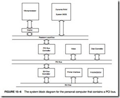
Figure 15–6 shows the system structure for the PCI bus in a personal computer system. Notice that the microprocessor bus is separate and independent of the PCI bus. The microprocessor

Bus Interface-0327

connects to the PCI bus through an integrated circuit called a PCI bridge. This means that virtually any microprocessor can be interfaced to the PCI bus, as long as a PCI controller or bridge is designed for the system. In the future, all computer systems may use the same bus. Even the Apple Macintosh system is switching to the PCI bus. The resident local bus is often called a front side bus.

The PCI Bus Pin-Out

As with the other buses described in this chapter, the PCI bus contains all of the system control signals. Unlike the other buses, the PCI bus functions with either a 32-bit or a 64-bit data bus and a full 32-bit address bus. Another difference is that the address and data buses are multiplexed to reduce the size of the edge connector. These multiplexed pins are labeled AD0–AD63 on the connector. The 32-bit card (which is found in most computers) has only connections 1 through 62, while the 64-bit card has all 94 connections. The 64-bit card can accommodate a 64-bit address if it is required at some point in the future. Figure 15–7 on the next page illustrates the PCI bus pin-out.

As with the other bus systems, the PCI bus is most often used for interfacing I/O components to the microprocessor. Memory could be interfaced, but it would operate only at a 33 MHz rate with the Pentium, which is half the speed of the 66 MHz resident local bus of the Pentium system. A more recent version of PCI (2.1-compliant) operates at 66 MHz and at 33 MHz for older interface cards. Pentium 4 systems use a 200 MHz system bus speed (although it is often listed as 800 MHz), but there is no planned modification to the PCI bus speed yet.

The PCI Address/Data Connections

The PCI address appears on AD0–AD31 and it is multiplexed with data. In some systems, there is a 64-bit data bus that uses AD32–AD63 for data transfer only. In the future, these pins can be used for extending the address to 64 bits. Figure 15–8 illustrates the timing diagram for the PCI bus, which shows the way that the address is multiplexed with data and also the control signals used for multiplexing.

During the first clocking period, the address of the memory or I/O location appears on the AD connections, and the command to a PCI peripheral appears on the C>BE pins. Table 15–4 illustrates the bus commands found on the PCI bus.

INTA Sequence During the interrupt acknowledge sequence, an interrupt controller (the controller that caused the interrupt) is addressed and interrogated for the interrupt vector. The byte-sized interrupt vector is returned during a byte read operation.

Bus Interface-0328Bus Interface-0329

Special Cycle The special cycle is used to transfer data to all PCI components.

During this cycle, the rightmost 16 bits of the data bus contain a 0000H, indicating a processor shutdown, 0001H for a processor halt, or 0002H for 80X86 specific code or data.

I/O Read Cycle Data are read from an I/O device using the I/O address that appears on AD0–AD15. Burst reads are not supported for I/O devices.

I/O Write Cycle As with I/O read, this cycle accesses an I/O device, but writes data.

Bus Interface-0330

FIGURE 15–8 The basic burst mode timing for the PCI bus system. Note that this transfers either four 32-bit numbers (32-bit PCI) or four 64-bit numbers (64-bit PCI).

Memory Read Cycle Data are read from a memory device located on the PCI bus.

Memory Write Cycle As with memory read, data are accessed in a device located on the PCI bus. The location is written.

Configuration Read Configuration information is read from the PCI device using the

configuration read cycle.

Configuration Write The configuration write allows data to be written to the configuration area in a PCI device. Note that the address is specified by the configuration read.

Memory Multiple This is similar to the memory read access, except that it is usually

Access used to access many data instead of one.

Dual Addressing Used for transferring address information to a 64-bit PCI device, Cycle which only contains a 32-bit data path.

Line Memory Used to read more than two 32-bit numbers from the PCI bus.

Addressing

Memory Write with This is the same as line memory access, but it is used with a write.

Invalidation This write bypasses the write-back function of the cache.

Configuration Space

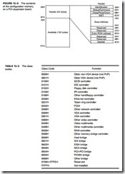
The PCI interface contains a 256-byte configuration memory that allows the computer to interrogate the PCI interface. This feature allows the system to automatically configure itself for the PCI plug-board. Microsoft Corporation calls this plug-and-play (PnP). Figure 15–9 illustrates the configuration memory and its contents.

The first 64 bytes of the configuration memory contain the header that holds information about the PCI interface. The first 32-bit doubleword contains the unit ID code and the vendor ID code. The unit ID code is a 16-bit number (D31–D16) that is an FFFFH if the unit is not installed, and a number between 0000H and FFFEH that identifies the unit if it is installed. The class codes identify the class of the PCI interface. The class code is found in bits D31–D16 of configuration memory at location 08H. Note that bits D15–D0 are defined by the manufacturer. The current

Bus Interface-0331Bus Interface-0332

class codes are listed in Table 15–5 and are assigned by the PCI SIG, which is the governing body for the PCI bus interface standard. The vendor ID (D15–D0) is also allocated by the PCI SIG.

The status word is loaded in bits D31–D16 of configuration memory location 04H and the command is at bits D15–D0 of location 04H. Figure 15–10 illustrates the format of both the status and command registers.

The base address space consists of a base address for the memory, a second for the I/O space, and a third for the expansion ROM. The first two doublewords of the base address space contain either the 32- or 64-bit base address for the memory present on the PCI interface. The next doubleword contains the base address of the I/O space. Note that even though the Intel microprocessors only use a 16-bit I/O address, there is room for expanding the I/O address to 32 bits. This allows systems that use the 680X0 family and PowerPC access to the PCI bus because they do have I/O space that is accessed via a 32-bit address. The 600X0 and PowerPC use memory-mapped I/O, discussed at the beginning of Chapter 11.

BIOS for PCI

Most modem personal computers contain the PCI bus and an extension to the normal system BIOS that supports the PCI bus. These newer systems contain access to the PCI bus at interrupt vector 1AH. Table 15–6 lists the functions currently available through the DOS INT 1AH instruction with AH = 0B1H for the PCI bus.

Example 15–5 shows how the BIOS is used to determine whether the PCI bus extension available. Once the presence of the BIOS is established, the contents of the configuration memory can be read using the BIOS functions. Note that the BIOS does not support data transfers between the computer and the PCI interface. Data transfers are handled by drivers that are pro- vided with the interface. These drivers control the flow of data between the microprocessor and the component found on the PCI interface.

Bus Interface-0333Bus Interface-0334Bus Interface-0335

PCl Interface

The PCI interface is complex, and normally an integrated PCI bus controller is used for interfacing to the PCI bus. It requires memory (EPROM) to store vendor information and other information, as explained earlier in this section of the chapter. The basic structure of the PCI interface is illustrated in Figure 15–11. The contents of this block diagram illustrate the required components for a functioning PCI interface; it does not illustrate the interface itself. The Registers, Parity Block, Initiator, Target, and Vendor ID EPROM are required components of any PCI interface. If a PCI interface is constructed, a PCI controller is often used because of the complexity of this interface. The PCI con- troller provides the structures shown in Figure 15–11.

PCI Express Bus

The PCI Express transfers data in serial at the rate of 2.5 GHz to legacy PCI applications, increasing the data link speed to 250 MBps to 8 GBps for PCI Express interfaces. The standard PCI bus delivers data at a speed of about 133 MBps, in comparison. The big improvement is on the moth- erboard, where the interconnections are in serial and at 2.5 GHz. Each serial connection on the PCI Express bus is called a lane. The slots on the main board are single lane slots with a total transfer speed of 1 GBps. The PCI Express video card connector currently has 16 lanes with a

Bus Interface-0336Bus Interface-0337

transfer speed of 4 GBps. The standard allows up to 32 lanes, but at present the widest slot is the 16 lanes on the video card. Most current main boards contain four single lane slots for peripherals and one 16 lane slot for the video card. A few newer main boards contain two 16 lane slots. In the future the standard PCI slots will all be replaced with the lower cost PCI Express connectors.

The PCI Express 2 bus was released in late 2007 with a transfer speed that is twice that of the PCI Express bus. This means that the speed per lane increased from 250 MBps to 500 MBps.

This new version of the PCI bus is replacing most current video cards on the AGP port with a yet higher speed version of the PCI Express bus. This technology (serial) allows main board manufacturers to use less space on the main board for interconnection and thus reduce the cost of manufacturing a main board. The connectors are smaller, which also reduces connector cost. The software used with the PCI Express bus remains the same as that used with the PCI bus so new programs are not needed to develop drivers for the PCI Express bus.

The PCI Express pin-out for the most commonly interfaced connector, the single lane connector, appears in Table 15–7. The connector is a 36-pin connector as illustrated in Figure 15–12. Signaling on the PCI Express bus uses 3.3 V with differential signals that are 180 degrees

Bus Interface-0338

out of phase. The lane is constructed from a pair of data pipes, one for input data and one for output data.


BUS INTERFACE:BUS INTERFACE.

BUS INTERFACE

INTRODUCTION

Many applications require some knowledge of the bus systems located within the personal computer. At times, main boards from personal computers are used as core systems in industrial applications. These systems often require custom interfaces that are attached to one of the buses on the main board. This chapter presents the ISA (industry standard architecture) bus, the PCI (peripheral component interconnect) and PCI Express buses, the USB (universal serial bus), and the AGP (advanced graphics port). Also provided are some simple interfaces to many of these bus systems as design guides.

Although it is likely that they will not be on personal computers of the future, the parallel port and serial communications ports are discussed. These were the first I/O ports on the per- sonal computer and they have stood the test of time, but the universal serial bus seems to have all but replaced their utility.

CHAPTER OBJECTIVES

Upon completion of this chapter, you will be able to:

1. Detail the pin connections and signal bus connections on the parallel and serial ports as well as on ISA, AGP, PCI, and PCI Express buses.

2. Develop simple interfaces that connect to the parallel and serial ports and the ISA and PCI buses.

3. Program interfaces located on boards that connect to the ISA and PCI buses.

4. Describe the operation of the USB and develop some short programs that transfer data.

5. Explain how the AGP increases the efficiency of the graphics subsystem.

THE ISA BUS

The ISA, or industry standard architecture, bus has been around since the very start of the IBM- compatible personal computer system (circa 1982). In fact, any card from the very first personal computer will plug into and function in any of the modern Pentium 4-based computers provided they have an ISA slot. This is all made possible by the ISA bus interface found in some of these machines, which is still compatible with the early personal computers. The ISA bus has all but disappeared on the home PC, but is still found in many industrial applications and is presented here for this reason. The main reason it is still used in industrial application is the low cost of the interface and the number of existing interface cards. This will eventually change.

Evolution of the ISA Bus

The ISA bus has changed from its early days. Over the years, the ISA bus has evolved from its original 8-bit standard to the 16-bit standard found in some systems today. The last computer system that contained the ISA bus en masse was the Pentium III. When the Pentium 4 started to appear, the ISA bus started to disappear. Along the way, there was even a 32-bit version called the EISA bus (extended ISA), but that seems to have all but disappeared. What remains today in some personal computers is an ISA slot (connection) on the main board that can accept either an 8-bit ISA card or a 16-bit ISA printed circuit card. The 32-bit printed circuit cards are the PCI bus or, in some older 80486-based machines, the VESA cards. The ISA bus has all but vanished recently in home computers, but it is available as a special order in most main boards. The ISA bus is still found in many industrial applications, but its days now seem limited.

The 8-Bit ISA Bus Output Interface

Figure 15–1 illustrates the 8-bit ISA connector found on the main board of all personal computer systems (again, this may be combined with a 16-bit connector). The ISA bus connector contains the entire demultiplexed address bus (A19–A0) for the 1M-byte 8088 system, the 8-bit data bus (D7–D0), and the four control signals MEMR, MEMW, IOR, and IOW for controlling I/O and any memory that might be placed on the printed circuit card. Memory is seldom added to any

Bus Interface-0315

ISA bus card today because the ISA card only operates at an 8 MHz rate. There might be an EPROM or flash memory used for setup information on some ISA cards, but never any RAM.

Other signals, which are useful for I/O interface, are the interrupt request lines IRQ2–IRQ7. Note that IRQ2 is redirected to IRQ9 on modern systems and is so labeled on the connector in Figure 15–1. The DMA channels 0–3 control signals are also present on the con- nector. The DMA request inputs are labeled DRQ1–DRQ3 and the DMA acknowledge outputs are labeled DACK0 – DACK3. Notice that the DRQ0 input pin is missing because the early per- sonal computers used it and the DACK0 output as a refresh signal to refresh any DRAM that might be located on the ISA card. Today, this output pin contains a 15.2 μs clock signal that was used for refreshing DRAM. The remaining pins are for power and RESET.

Suppose that a series of four 8-bit latches must be interfaced to the personal computer for 32 bits of parallel data. This is accomplished by purchasing an ISA interface card (part number 4713-1) from a company like Vector Electronics or other companies. In addition to the edge con- nector for the ISA bus, the card also contains room at the back for interface connectors. A 37-pin subminiature D-type connector can be placed on the back of the card to transfer the 32 bits of data to the external source.

Figure 15–2 shows a simple interface for the ISA bus, which provides 32 bits of parallel TTL data. This example system illustrates some important points about any system interface. First, it is extremely important that the loading to the ISA bus be kept to one low-power (LS) TTL load. In this circuit, a 74LS244 buffer is used to reduce the loading on the data bus. If the

Bus Interface-0316Bus Interface-0317

74LS244 were not there, this system would present the data bus with four unit loads. If all bus cards were to present heavy loads, the system would not operate properly (or perhaps not at all).

Output from the ISA card is provided in this circuit by a 37-pin connector labeled P1. The output pins from the circuit connect to P1, and a ground wire is attached. You must provide ground to the outside world, or else the TTL data on the parallel ports are useless. If needed, the output control pins 1OC2 on each of the 74LS374 latch chips can also be removed from ground and connected to the four remaining pins on P1. This allows an external circuit to control the out- puts from the latches.

A small DIP switch is placed on two of the outputs of D7, so the address can be changed if an address conflict occurs with another card. This is unlikely, unless you plan to use two of these cards in the same system. Address connection A2 is not decoded in this system so it becomes a don’t care (x). See Table 15–1 for the addresses of each latch and each position of the S1. Note that only one of the two switches may be on at a time and that each port has two possible addresses for each switch setting because A2 is not connected.

In the personal computer, the ISA bus is designed to operate at I/O address 0000H through 03FFH. Depending on the version and manufacturer of the main board, ISA cards may or may not function above these locations. Some newer systems often allow ISA ports at locations above 03FFH, but older systems do not. The ports in this example may need to be changed for some systems. Some older cards only decode I/O addresses 0000H–03FFH and may have address con- flicts if the port addresses above 03FFH conflict. The ports are decoded in this example by three 74LS138 decoders. It would be more efficient and cost-effective to decode the ports with a pro- grammable logic device.

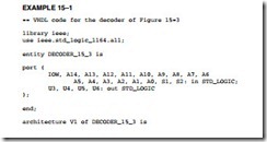
Figure 15–3 shows the circuit of Figure 15–2 reworked using a PLD to decode the addresses for the system. Notice that address bits A15–A4 are decoded by the PLD and the switch is connected to two of the PLD inputs. This change allows four different I/O port addresses for each latch, making the circuit more flexible. Table 15–2 shows the port number selected by switch 1–4 and switch 2–3. Example 15–1 shows the program for the PLD that causes the port assignments of Table 15–2.

Bus Interface-0318Bus Interface-0319Bus Interface-0320

Notice in Example 15–1 how the first term (U3) generates a logic 0 on the output to the decoder only when both switches are in their off positions for I/O port 0300H. It also generates a clock for U3 for I/O ports 304H, 308H, or 30CH, depending on the switch settings. The second term (U4) is active for ports 301H, 305H, 309H, or 30DH, depending on the switch settings. Again, refer to Table 15–2 for the complete set of port assignments for various switch settings. Since A15 is connected to the bottom of the switches, this circuit will also activate the latches for other I/O locations, because it is not decoded. I/O addresses 830XH will also generate clock sig- nals to the latch because A15 is not decoded.

Example 15–2 shows two C++ functions that transfer an integer to the 32-bit port. Either of these functions sends data to the port; the first is more efficient, but the second may be more readable. (Example 15–2(c) shows Example 15–2(b) in disassembled form.) Two parameters are passed to the function: One is the data to be sent to the port, and the other is the base port address. The base address is 0300H, 0304H, 0308H, or 030CH and must match the switch settings of Figure 15–3.

Bus Interface-0321Bus Interface-0322

The 8-Bit ISA Bus Input Interface

To illustrate the input interface to the ISA bus, a pair of ADC804 analog-to-digital converters are interfaced to the ISA bus in Figure 15–4. The connections to the converters are made through a nine-pin DB9 connector. The task of decoding the I/O port addresses is more complex, because each converter needs a write pulse to start a conversion, a read pulse to read the digital data once they have been converted from the analog input data, and a pulse to enable the selection of the INTR output. Notice that the INTR output is connected to data bus bit position D0. When INTR is

Bus Interface-0323Bus Interface-0324

input to the microprocessor, the rightmost bit of AL is tested to determine whether the converter is busy.

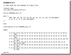
As before, great care is taken so that the connections to the ISA bus present one unit load to the system. Table 15–3 illustrates the I/O port assignment decoded by the PLD (see Example 15–3 for the program). In this example we assumed that the standard ISA bus is used, which only contains address connection A0 through A9.

Bus Interface-0325

Example l5–4 lists a function that can read either ADC U3 or U4. The address is generated by passing either a 0 for U3 or a 1 for U4 to the address parameter of the function. The function starts the converter by writing to it, and then waits until the INTR pin returns to a logic 0, indicating that the conversion is complete before the data are read and returned by the function as a char.

Bus Interface-0326

of the additional connector and its placement in the computer in relation to the 8-bit connector. Unless additional memory is added on the ISA card, the extra address connections A23–A20 do not serve any function for I/O operations. The added features that are most often used are the additional interrupt request inputs and the DMA request signals. In some systems, 16-bit I/O uses the additional eight data bus connections (D8–D15), but more often today the PCI bus is used for peripherals that are wider than 8 bits. About the only recent interfaces found for the ISA bus are a few modems and sound cards.


QUESTIONS AND PROBLEMS ON THE ARITHMETIC COPROCESSOR, MMX, AND SIMD TECHNOLOGIES.

QUESTIONS AND PROBLEMS

1. List the three types of data that are loaded or stored in memory by the coprocessor.

2. List the three integer data types, the range of the integers stored in them, and the number of bits allotted to each.

3. Explain how a BCD number is stored in memory by the coprocessor.

4. List the three types of floating-point numbers used with the coprocessor and the number of binary bits assigned to each.

5. Convert the following decimal numbers into single-precision floating-point numbers:

(a) 28.75

(b) 624

(c) – 0.615

(d) + 0.0

(e) – 1000.5

6. Convert the following single-precision floating-point numbers into decimal:

(a) 11000000 11110000 00000000 00000000

(b) 00111111 00010000 00000000 00000000

(c) 01000011 10011001 00000000 00000000

(d) 01000000 00000000 00000000 00000000

(e) 01000001 00100000. 00000000 00000000

(f) 00000000 00000000 00000000 00000000

7. Explain what the coprocessor does when a normal microprocessor instruction executes.

8. Explain what the microprocessor does when a coprocessor instruction executes.

9. What is the purpose of the C3–C0 bits in the status register?

10. What operation is accomplished with the FSTSW AX instruction?

11. What is the purpose of the IE bit in the status register?

12. How can SAHF and a conditional jump instruction be used to determine whether the top of the stack (ST) is equal to register ST(2)?

13. How is the rounding mode selected in the 80X87?

14. What coprocessor instruction uses the microprocessor’s AX register?

15. What I/O ports are reserved for coprocessor use with the 80287?

16. How are data stored inside the coprocessor?

17. What is a NAN?

18. Whenever the coprocessor is reset, the top of the stack register is register number

19. What does the term chop mean in the rounding control bits of the control register?

20. What is the difference between affine and projective infinity control?

21. What microprocessor instruction forms the opcodes for the coprocessor?

22. The FINIT instruction selects -precision for all coprocessor operations.

23. Using assembler pseudo-opcodes, form statements that accomplish the following:

(a) Store a 23.44 into a double-precision floating-point memory location FROG.

(b) Store a –123 into a 32-bit signed integer location DATA3.

(c) Store a –23.8 into a single-precision floating-point memory location DATAL.

(d) Reserve double-precision memory location DATA2.

24. Describe how the FST DATA instruction functions. Assume that DATA is defined as a 64-bit memory location.

25. What does the FILD DATA instruction accomplish?

26. Form an instruction that adds the contents of register 3 to the top of the stack.

27. Describe the operation of the FADD instruction.

28. Choose an instruction that subtracts the contents of register 2 from the top of the stack and stores the result in register 2.

29. What is the function of the FBSTP DATA instruction?

30. What is the difference between a forward and a reverse division?

31. What is the purpose of the Pentium Pro FCOMI instruction?

32. What does a Pentium Pro FCMOVB instruction accomplish?

33. What must occur before executing any FCMOV instruction?

34. Develop a procedure that finds the reciprocal of the single-precision floating-point number.

The number is passed to the procedure in EAX and must be returned as a reciprocal in EAX.

35. What is the difference between the FTST instruction and FXAM?

36. Explain what the F2XM1 instruction calculates.

37. Which coprocessor status register bit should be tested after the FSQRT instruction exe- cutes?

38. Which coprocessor instruction pushes π onto the top of the stack?

39. Which coprocessor instruction places 1.0 at the top of the stack?

40. What will FFREE ST(2) accomplish when executed?

41. Which instruction stores the environment?

42. What does the FSAVE instruction save?

43. Develop a procedure that finds the area of a rectangle (A = L × W). Memory locations for this procedure are single-precision floating-point locations A, L, and W.

44. Write a procedure that finds the capacitive reactance Memory locations for this procedure are single-precision floating-point locations XC, F, and C1 for C.

45. Develop a procedure that generates a table of square roots for the integers 2 through 10. The results must be stored as single-precision floating-point numbers in an array called ROOTS.

46. When is the FWAIT instruction used in a program?

47. What is the difference between the FSTSW and FNSTSW instructions?

48. Given the series/parallel circuit and equation illustrated in Figure 14–17, develop a program using single-precision values for R1, R2, R3, and R4 that finds the total resistance and stores the result at single-precision location RT.

49. Develop a procedure that finds the cosine of a single-precision floating-point number. The angle, in degrees, is passed to the procedure in EAX and the cosine is returned in EAX. Recall that FCOS finds the cosine of an angle expressed in radians.

50. Given two arrays of double-precision floating-point data (ARRAY1 and ARRAY2) that each contain 100 elements, develop a procedure that finds the product of ARRAY1 times ARRAY2, and then stores the double-precision floating-point result in a third array (ARRAY3).

The Arithmetic Coprocessor, MMX,and SIMD Technologies-0313

51. Develop a procedure that takes the single-precision contents of register EBX times π and stores the result in register EBX as a single-precision floating-point number. You must use memory to accomplish this task.

52. Write a procedure that raises a single-precision floating-point number X to the power Y. Parameters are passed to the procedure with EAX = X and EBX = Y. The result is passed back to the calling sequence in ECX.

53. Given that the LOG10 X = (LOG2 10)-1 × LOG2 X, write a procedure called LOG10 that finds the LOG10 of the value (X) at the stack top. Return the LOG10 at the stack top at the end of the procedure.

54. Use the procedure developed in question 53 to solve the equation Gain in decibels = 20log Vout 10 Vin

54. The program should take arrays of single-precision values for Vout and Vin and store the decibel gains in a third array called DBG. These are 100 values Vout and Vin.

55. What is the MMX extension to the Pentium–Core2 microprocessors?

56. What is the purpose of the EMMS instruction?

57. Where are the MM0–MM7 registers found in the microprocessor?

58. What is signed saturation?

59. What is unsigned saturation?

60. How could all of the MMX registers be stored in the memory with one instruction?

61. Write a short program that uses MMX instruction to multiply the word-size numbers in arrays and store the 32-bit results in a third array. The source arrays are 256 words long.

62. What are SIMD instructions?

63. What are SSE instructions?

64. The XMM registers are bits wide.

65. A single XMM register can hold single-precision floating-point numbers.

66. A single XMM register can hold byte-sized integers.

67. What is an OWORD?

68. Can floating-point instructions for the arithmetic coprocessor execute at the same time as SSE instructions?

69. Develop a C++ function (using inline assembly code) that computes (using scalar SSE instructions and floating-point instructions) and returns a single-precision number that rep- resents the resonant frequency from parameters (L and C) passed to it to solve the following equation:

The Arithmetic Coprocessor, MMX,and SIMD Technologies-0314


THE ARITHMETIC COPROCESSOR, MMX, AND SIMD TECHNOLOGIES:INTRODUCTION TO SSE TECHNOLOGY.

INTRODUCTION TO SSE TECHNOLOGY

The latest type of instruction added to the instruction set of the Pentium 4 is SIMD (single- instruction multiple data). As the name implies, a single instruction operates on multiple data in much the same way as do the MMX instructions, which are SIMD instructions that operate on multiple data. The MMX instruction set functions with integers; the SIMD instruction set functions with floating-point numbers as well as integers. The SIMD extension instructions first appeared in the Pentium III as SSE (streaming SIMD extensions) instructions. Later, SSE 2 instructions were added to the Pentium 4, and new to the Pentium 4 (beginning with the 90- nanometer E model) are SSE 3 instructions. The SSE 3 extensions are also found in the Core2 microprocessor.

Recall that the MMX instructions shared registers with the arithmetic coprocessor. The SSE instructions use a new and separate register array to operate on data. Figure 14–13 illustrates an array of eight 128-bit-wide registers that function with the SSE instructions. These new registers

The Arithmetic Coprocessor, MMX,and SIMD Technologies-0305

are called XMM registers (XMM0–XMM7), which denote extended multimedia registers. To accommodate this new 128-bit-wide data size, a new keyword is added called OWORD. An OWORD (octalword) designates a 128-bit variable, as in OWORD PTR for the SSE instruction set. A double quadword is also used at times to specify a 128-bit number.

Just as the MMX registers can contain multiple data types, so can the XMM registers of the SSE unit. Figure 14–14 illustrates the data types that can appear in any XMM register for various SSE instructions. An XMM register can hold four single-precision floating-point numbers or two double-precision floating-point numbers. XMM registers can also hold six- teen 8-bit integers, eight 16-bit integers, four 32-bit integers, or two 64-bit integers. This is a twofold increase in the capacity of the system when compared to the integers contained in MMX registers and hence a twofold increase in execution speeds of integers operations that use the XMM registers and SSE instructions. For new applications that are designed to exe- cute on a Pentium 4 or newer microprocessor, the SSE instructions are used in place of the MMX instructions. Because not all machines are yet Pentium 4 class machines, there still is a need to include MMX technology instructions in a program for compatibility to these older systems.

Floating-Point Data

Floating point data are operated upon as either packed or scalar, and either single-precision or double-precision. The packed operation is performed on all sections at a time; the scalar form is only operated on the rightmost section of the register contents. Figure 14–15 shows both the packed and scalar operations on SSE data in XMM registers. The scalar form is comparable to

The Arithmetic Coprocessor, MMX,and SIMD Technologies-0306

the operation performed by the arithmetic coprocessor. Opcodes are appended with PS (packed single), SS (scalar single), PD (packed double), or SD (scaled double) to form the desired instruction. For example, the opcode for a multiply is MUL, but the opcode for a packed double is MULPD and MULSD for a scalar double multiplication. The single-precision multiplies are MULPS and MULSS. In other words, once the two-letter extension and its meaning are under- stood, it is relatively easy to master the new SSE instructions.

The Instruction Set

The SSE instructions have a few new types added to the instruction set. The floating-point unit does not have a reciprocal instruction, which is used quite often to solve complex equations. The reciprocal instruction (1) now appears in the SSE extensions as the RCP instruction, which generates reciprocals and is written as RCPPS, RCPSS, RCPPD, and RCPSD. There is also a recip- rocal of a square root ( 1 ) instruction, called RSQRT, which is written as RSQRTPS, RSQRTSS, RSQRTPD, and RSQRTSD.

The remainder of the instructions for the SSE unit are basically the same as for the micro- processor and MMX unit except for a few cases. The instruction table in Appendix B lists the instructions, but does not list the extensions (PS, SS, PD, and DS) to the instructions. Again note

The Arithmetic Coprocessor, MMX,and SIMD Technologies-0307

that SSE 2 and SSE 3 contain double-precision operations and SSE does not. Instructions that start with the letter P operate on integer data that is byte, word, doubleword, or quadword sized. For example, the PADDB XMM0, XMM1 instruction adds the 16 byte-sized integers in the XMM1 register to the 16 byte-sized integers in the XMM0 register. PADDW adds 16-bit integers, PADDD adds doublewords, and PADDQ adds quadwords. The execution times are not provided by Intel so they do not appear in the appendix for these instructions.

The Control/Status Register

The SSE unit also contains a control/status register accessed as MXCSR. Figure 14–16 illustrates the MXCSR for the SSE unit. Notice that this register is very similar to the control/status register of the arithmetic coprocessor presented earlier in this chapter. This register sets the precision and rounding modes for the coprocessor, as does the control register for the arithmetic coprocessor, and it provides information about the operation the SSE unit.

The SSE control/status register is loaded from memory using the LDMXCSR and FXRSTOR instructions or stored into the memory using the STMXCSR and FXSAVE instructions. Suppose the rounding control (see Figure 14–6 for the state of the rounding control bits) needs to be changed to round toward positive infinity (RC = 10). Example 14–14 shows the soft- ware that changes only the rounding control bits of the control/status register.

The Arithmetic Coprocessor, MMX,and SIMD Technologies-0308

Programming Examples

A few programming examples are needed to show how to use the SSE unit. As mentioned, the SSE unit allows floating-point and integer operations on multiple data. Suppose that the capacitive

reactance is needed for a circuit that contains a 1.0 μF capacitor at various frequencies from 100 Hz to 10,000 Hz in 100 Hz steps. The equation used to calculate capacitive reactance is:

The Arithmetic Coprocessor, MMX,and SIMD Technologies-0309

Example 14–15 illustrates a procedure that generates the 100 outcomes for this equation using the SSE unit and single-precision floating-point data. The program listed in Example 14–15(a) uses the SSE unit to perform four calculations per iteration, while the program in Example 14–15(b) uses the floating-point coprocessor to calculate XC one at a time. Example 14–15(c) is yet another example in C++. Examine the loop to see that the first exam- ple goes through the loop 25 times and the second goes through the loop 100 times. Each time the loop executes in Example 14–15(a) it executes seven instructions (25 × 7 = 175), which takes 175 instruction times. Example 14–15(b) executes eight instructions per iteration of its loop (100 × 8 = 800), which requires 800 instruction times. By using this parallelism, the SSE unit allows the calculations to be accomplished in much less time than any other method. The C++ version in Example 14–15(c) uses the directive __declspec(align(16)) before each variable to make certain that they are aligned properly in the memory. If these are missing, the program will not function because the SSE memory variables must be aligned on at least quadword boundaries (16). This final version executes at about 41/2 times faster than Example 14–15(b);

The Arithmetic Coprocessor, MMX,and SIMD Technologies-0310The Arithmetic Coprocessor, MMX,and SIMD Technologies-0311

The first example in this section (Example 14–15) used floating-point number to perform multiple calculations, but the SSE unit can also operate on integers. The example illustrated in Example 14–16 uses integer operation to add BlockA to BlockB and store the sum in BlockC. Each block contains 4000 eight-bit numbers. Example 14–16(a) lists an assembly language procedure that forms the sums using the standard integer unit of the microprocessor, which requires 4000 iterations to accomplish.

The Arithmetic Coprocessor, MMX,and SIMD Technologies-0312

Both example programs generate 4000 sums, but the second example using the SSE unit does it by passing through its loop 250 times, while the first example requires 4000 passes. Hence, the second example functions 16 times faster because of the SSE unit. Notice how the PADDB (an instruction presented with the MMX unit) is used with the SSE unit. The SSE unit uses the same commands as the MMX except the registers are different. The MMX unit uses 64-bit-wide MM registers and the SSE unit uses 128-bit-wide XMM registers.

Optimization

The compiler in Visual C++ does have optimization for the SSE unit, but it does not optimize the examples presented in this chapter. It will attempt to optimize a single equation in a statement if the SSE unit can be utilized for the equation. It does not look at a program for blocks of operations that can be optimized as in the examples presented here. Until a compiler and extensions are developed so parallel operations such as these can be included, programs that require high speeds will require hand-coded assembly language for optimization. This is especially true of the SSE unit.


SUMMARY OF THE ARITHMETIC COPROCESSOR, MMX, AND SIMD TECHNOLOGIES.

SUMMARY

1. The arithmetic coprocessor functions in parallel with the microprocessor. This means that the microprocessor and coprocessor can execute their respective instructions simultaneously.

2. The data types manipulated by the coprocessor include signed integer, floating-point, and binary-coded decimal (BCD).

3. Three forms of integers are used with the coprocessor: word (16 bits), short (32 bits), and long (64 bits). Each integer contains a signed number in true magnitude for positive numbers and two’s complement form for negative numbers.

4. A BCD number is stored as an 18-digit number in 10 bytes of memory. The most significant byte contains the sign-bit, and the remaining nine bytes contain an 18-digit packed BCD number.

5. The coprocessor supports three types of floating-point numbers: single-precision (32 bits), double-precision (64 bits), and temporary extended-precision (80 bits). A floating-point number has three parts: the sign, biased exponent, and significant. In the coprocessor, the exponent is biased with a constant and the integer bit of the normalized number is not stored in the significant, except in the temporary extended-precision form.

6. Decimal numbers are converted to floating-point numbers by (a) converting the number to binary, (b) normalizing the binary number, (c) adding the bias to the exponent, and (d) stor- ing the number in floating-point form.

7. Floating-point numbers are converted to decimal by (a) subtracting the bias from the expo- nent, (b) un-normalizing the number, and (c) converting it to decimal.

8. The 80287 uses I/O space for the execution of some of its instructions. This space is invisible to the program and is used internally by the 80286/80287 system. These 16-bit I/O addresses (00F8H–00FFH) must not be used for I/O data transfers in a system that contains an 80287. The 80387, 80486/7, and Pentium through Core2 use I/O addresses 800000F8H–800000FFH.

9. The coprocessor contains a status register that indicates busy, the conditions that follow a compare or test, the location of the top of the stack, and the state of the error bits. The FSTSW AX instruction, followed by SAHF, is often used with conditional jump instructions to test for some coprocessor conditions.

10. The control register of the coprocessor contains control bits that select infinity, rounding, precision, and error masks.

11. The following directives are often used with the coprocessor for storing data: DW (defineword), DD (define doubleword), DQ (define quadword), and DT (define 10 bytes).

12. The coprocessor uses a stack to transfer data between itself and the memory system. Generally, data are loaded to the top of the stack or removed from the top of the stack for storage.

13. All internal coprocessor data are always in the 80-bit extended-precision form. The only time that data are in any other form is when they are stored or loaded from the memory.

14. The coprocessor addressing modes include the classic stack mode, register, register with apop, and memory. Stack addressing is implied. The data at ST become the source, at ST(1) the destination, and the result is found in ST after a pop.

15. The coprocessor’s arithmetic operations include addition, subtraction, multiplication, divi- sion, and square root calculation.

16. There are transcendental functions in the coprocessor’s instruction set. These functions find the partial tangent or arctangent, 2X – 1, Y log2 X, and Y log2 (X + 1). The 80387, 80486/7,

and Pentium–Core2 also include sine and cosine functions.

17. Constants are stored inside the coprocessor that provide +0.0, +1.0, π, log2 10, log2 ε, log2 2, and logε 2.

18. The 80387 functions with the 80386 microprocessor and the 80487SX functions with the 80486SX microprocessor, but the 80486DX and Pentium–Core2 contain their own internal arithmetic coprocessor. The instructions performed by the earlier versions are available on these coprocessors. In addition to these instructions, the 80387, 80486/7, and Pentium–Core2 also can find the sine and cosine.

19. The Pentium Pro through Core2 contain two new floating-point instructions: FCMOV and FCOMI. The FCMOV instruction is a conditional move and the FCOMI performs the same task as FCOM, but it also places the floating-point flags into the system flag register.

20. The MMX extension uses the arithmetic coprocessor registers for MM0–MM7. Therefore, it is important that coprocessor software and MMX software do not try to use them at the same time.

21. The instructions for the MMX extensions perform arithmetic and logic operations on bytes (eight at a time), words (four at a time), doublewords (two at a time), and quadwords. The operations performed are addition, subtraction, multiplication, division, AND, OR, Exclusive-OR, and NAND.

22. Both the MMX unit and the SSE unit employ SIMD techniques to perform parallel opera- tions on multiple data with a single instruction. The SSE unit performs operations on inte- gers and floating-point numbers. The registers in the SSE unit are 128 bits in width and can hold (SSE 2 or newer) 16 bytes at a time or four single-precision floating-point numbers. The SSE unit contains registers XMM0–XMM7.

23. New applications written for the Pentium 4 should contain SSE instructions in place of

MMX instructions.

24. The OWORD pointer has been added to address 128-bit-wide numbers, which are referred to as octal words or double quadwords.


THE ARITHMETIC COPROCESSOR, MMX, AND SIMD TECHNOLOGIES:INTRODUCTION TO MMX TECHNOLOGY.

INTRODUCTION TO MMX TECHNOLOGY

The MMX1 (multimedia extensions) technology adds 57 new instructions to the instruction set of the Pentium–Pentium 4 microprocessors. The MMX technology also introduces new general- purpose instructions. The new MMX instructions are designed for applications such as motion video, combined graphics with video, image processing, audio synthesis, speech synthesis and compression, telephony, video conferencing, 2D graphics, and 3D graphics. These instructions (new beginning with the Pentium in 1995) operate in parallel with other operations as the instructions for the arithmetic coprocessor.

Data Types

The MMX architecture introduces new packed data types. The data types are eight packed, consecutive 8-bit bytes; four packed, consecutive 16-bit words; and two packed, consecutive 32-bit doublewords. Bytes in this multibyte format have consecutive memory addresses and use the little endian form, as with other Intel data. See Figure 14–11 for the format for these new data types.

The MMX technology registers have the same format as a 64-bit quantity in memory and have two data access modes: 64-bit access mode and 32-bit access mode. The 64-bit access mode is used for 64-bit memory and registers transfers for most instructions. The 32-bit access mode is used for 32-bit memory and also register transfers for most instructions. The 32-bit transfers occur between microprocessor registers, and the 64-bit transfers occur between floating-point coprocessor registers.

Figure 14–12 illustrates the internal register set of the MMX technology extension and how it uses the floating-point coprocessor register set. This technique is called aliasing because the floating-point registers are shared as the MMX registers. That is, the MMX registers (MM0–MM7) are the same as the floating-point registers. Note that the MMX register set is 64 bits wide and uses the rightmost 64 bits of the floating-point register set.

The Arithmetic Coprocessor, MMX,and SIMD Technologies-0294The Arithmetic Coprocessor, MMX,and SIMD Technologies-0295

Instruction Set

The instruction for MMX technology includes arithmetic, comparison, conversion, logical, shift, and data transfer instructions. Although the instruction types are similar to the microprocessor’s instruction set, the main difference is that the MMX instructions use the data types shown in Figure 14–11 instead of the normal data types used with the microprocessor.

Arithmetic Instructions. The set of arithmetic instructions includes addition, subtraction, multiplication, a special multiplication with an addition, and so on. Three additions exist. The PADD and PSUB instructions add or subtract packed signed or unsigned packed bytes, packed words, or packed doubleword data. The add instructions are appended with a B, W, or D to select the size, as in PADDB for a byte, PADDW for a word, and PADDD for a doubleword. The same is true for the PSUB instruction. The PMULHW and the PMULLW instructions perform multiplication on four pairs of l6-bit operands, producing 32-bit results. The PMULHW instruction multiplies the high-order l6 bits, and the PMULLW instruction multiplies the low-order 16 bits. The PMADDWD instruction multiplies and adds. After multiplying, the four 32-bit results are added to produce two 32-bit doubleword results.

The MMX instructions use operands just as the integer or floating-point instructions do. The difference is the register names (MM0–MM7). For example, the PADDB MM1, MM2 instruction adds the entire 64-bit contents of MM2 to MM1, byte by byte. The result is steered into MM1. When each 8-bit section is added, any carries generated are dropped. For example, the byte A0H added to the byte 70H produces the byte sum of 10H. The true sum is 110H, but the carry is dropped. Note that the second operand or source can be a memory location containing the 64-bit packed source or an MMX register. You might say that this instruction performs the same function as eight separate byte-sized ADD instructions! If used in an application, this certainly speeds execution of the application. Like PADD, PSUB also does not carry or borrow. The difference is that if an overflow or underflow occurs, the difference becomes 7FH (+127) for an overflow and 80H (–128) for an underflow. Intel calls this saturation, because these values rep- resent the largest and smallest signed bytes.

Comparison Instructions. There are two comparison instructions: PCMPEQ (equal) and PCMPGT (greater than). As with PADD and PSUB, there are three versions of each compare instruction: for example, PCMPEQUB (compares bytes), PCMPEQUW (compares words), and PCMPEQUD (compares doublewords). These instructions do not change the microprocessor flag bits; instead, the result is all ones for a true condition and all zeros for a false condition. For example, if the PCMPEQB MM2, MM3 instruction is executed and the least significant bytes of MM2 and MM3 = 10H and 11H, respectively, the result found in the least significant byte of MM2 is 00H. This indicates that the least significant bytes were not equal. If the least significant byte contained an FFH, it indicates that the two bytes were equal.

Conversion Instructions. There are two basic conversion instructions: PACK and PUNPCK. PACK is available as PACKSS (signed saturation) and PACKUS (unsigned saturation). PUN- PCK is available as PUNPCKH (unpack high data) and PUNPCKL (unpack low data). Similar to the prior instructions, these can be appended with B, W, or D for byte, word, and doubleword pack and unpack, but they must be used in combinations WB (word to byte) or DW (doubleword to word). For example, the PACKUSWB MM3, MM6 instruction packs the words from MM6 into bytes in MM3. If the unsigned word does not fit (too large) into a byte, the destination byte becomes an FFH. For signed saturation, we use the same values explained under addition.

Logic Instructions. The logic instructions are PAND (AND), PANDN (NAND), POR (OR), and PXOR (Exclusive-OR). These instructions do not have size extensions, and perform these bit-wise operations on all 64 bits of the data. For example, the POR MM2, MM3 instruction ORs all 64 bits of MM3 with MM2. The logical sum is placed into MM2 after the OR operation.

Shift Instruction. This instruction contains logical shifts and an arithmetic shift right instruction. The logic shifts are PSLL (left) and PSRL (right). Variations are word (W), doubleword (D), and quadword (Q). For example, the PSLLQ MM3,2 instruction shifts all 64 bits in MM3 left two places. Another example is the PSLLD MM3,2 instruction that shifts the two 32-bit double- words in MM3 left two places each.

The PSRA (arithmetic right shift) instruction functions in the same manner as the logical shifts, except that the sign-bit is preserved.

Data Transfer Instructions. There are two data transfer instructions: MOVED and MOVEQ. These instructions allow transfers between registers and between a register and memory. The MOVED instruction transfers 32 bits of data between an integer register or memory location and an MMX register. For example, the MOVED ECX, MM2 instruction copies the rightmost 32 bits of MM2 into ECX. There is no instruction to transfer the leftmost 32 bits of an MMX register. You could use a shift right before a MOVED to do the transfer.

The MOVEQ instruction copies all 64 bits of an MMX register between memory or another MMX register. The MOVEQ MM2, MM3 instruction transfers all 64 bits of MM3 into MM2. EMMS Instruction. The EMMS (empty MMX-state) instruction sets (11) all the tags in the floating-point unit, so the floating-point registers are listed as empty. The EMMS instruction must be executed before the return instruction at the end of any MMX procedure, or a subsequent floating-point operation will cause a floating-point interrupt error, crashing Windows or any other application. If you plan to use floating-point instructions within an MMX procedure, you must use the EMMS instruction before executing the floating-point instruction. All other MMX instructions clear the tags, which indicate that all floating-point registers are in use.

Instruction Listing. Table 14–10 lists all the MMX instructions with the machine code so these instructions can be used with the assembler. At present, MASM does not support these new instructions unless you have upgraded to the latest version (6.15). The latest version can be found in the Windows Driver Development Kit (Windows DDK), which is available for a small ship- ping charge from Microsoft Corporation. It is also available in Visual Studio Express (search for ML.EXE). Any MMX instruction can be used inside Visual C++ using the inline assembler.

Programming Example. Example 14–13 on p. 581 illustrates a simple programming example that uses the MMAX instructions to perform a task that takes eight times longer using normal microprocessor instruction. In this example an array of 1000 bytes of data (BLOCKA) is added to a second array of 1000 bytes (BLOCKB). The result is stored in a third array called BLOCKC. Example 14–13(a) lists a procedure that uses traditional assembly language to perform the addition and Example 14–13(b) shows the same process using MMX instructions.

The Arithmetic Coprocessor, MMX,and SIMD Technologies-0296The Arithmetic Coprocessor, MMX,and SIMD Technologies-0297The Arithmetic Coprocessor, MMX,and SIMD Technologies-0298The Arithmetic Coprocessor, MMX,and SIMD Technologies-0299The Arithmetic Coprocessor, MMX,and SIMD Technologies-0300The Arithmetic Coprocessor, MMX,and SIMD Technologies-0301The Arithmetic Coprocessor, MMX,and SIMD Technologies-0302The Arithmetic Coprocessor, MMX,and SIMD Technologies-0303The Arithmetic Coprocessor, MMX,and SIMD Technologies-0304