THE PENTIUM II, PENTIUM III, PENTIUM 4, AND CORE2 MICROPROCESSORS:THE PENTIUM 4 AND CORE2.

THE PENTIUM 4 AND CORE2

The most recent version of the Pentium Pro architecture microprocessor is the Pentium 4 micro- processor and recently the Core2 from Intel. The Pentium II, Pentium III, Pentium 4, and Core2 are all versions of the Pentium Pro architecture. The Pentium 4 was released initially in November 2000 with a speed of 1.3 GHz. It is currently available in speeds up to 3.8 GHz. Two packages are available for early versions of this integrated microprocessor, the 423-pin PGA and the 478-pin FC-PGA2. Both versions of the original issue of the Pentium 4 used the 0.18 micron technology for fabrication. The most recent versions use either the 0.13 micron technology or the 90 nm (0.09 micron) technology. Newer versions of the Pentium 4 use the LGA (leadless grid array) 775 package, which has 775 pins. Intel is currently developing a 45 nm technology for

The Pentium II, Pentium III, Pentium 4,and Core2 Microprocessors-0501

future products. As with earlier versions of the Pentium III, the Pentium 4 uses a 100 MHz memory bus speed, but because it is quad pumped, the bus speed can approach 400 MHz. More recent versions use the 133 MHz bus listed as 533 MHz because of quad pumping or 200 MHz listed as 800 MHz. Some newer versions use a 1033 MHz or 1333 MHz front side bus; another package called the LGA 771 has appeared in newer versions of the Xeon. Figure 19–5 illustrates the pin- out of the 423-pin PGA of the Pentium 4 microprocessor.

Memory Interface

The memory interface to the Pentium 4 typically uses the Intel 945, 965, or 975 chip set. These chip sets provide a dual-pipe memory bus to the microprocessor with each pipe interfaced to a 32-bit-wide section of the memory. The two pipes function together to comprise the 64-bit-wide data path to the microprocessor. Because of the dual-pipe arrangement, the memory must be populated with pairs of DDR2 memory devices operating at 600 MHz, 800 MHz, or 1033 MHz. According to Intel the DDR2 arrangement provides a 300% increase in speed over a memory populated with PC-100 memory.

The Pentium II, Pentium III, Pentium 4,and Core2 Microprocessors-0502

Intel has abandoned RDRAM in favor of DDR2 (double data rate) memory beginning with the 965 and 975 chip sets. Apparently the claim of a 300% increase in RDRAM speed failed to prove factual. In addition to the inclusion of support for DDR2, memory support for the serial ATA disk interface has also been added.

Newer chip sets such as the 945 and 965 contain the PCI Express interface and do not contain the AGP interface. The AGP interface is replaced by PCI Express for video support. IDE support remains for interface to legacy devices such as older HDD, CD-ROM, and DVD drives.

Register Set

The Pentium 4 and Core2 register set is nearly identical to all other versions of the Pentium except that the MMX registers are separate entities from the floating-point registers. In addition, eight 128-bit- wide XMM registers are added for use with the SIMD (single-instruction, multiple data) instructions as explained in Chapter 14 and the extended 128-bit packed doubled floating-point numbers.

You might think of the XMM registers as double-wide MMX registers that can hold a pair of 64-bit double-precision floating-point numbers or four single-precision floating-point numbers. Likewise they can also hold 16-byte-wide numbers as the MMX registers hold 8-byte-wide numbers. The XMM registers are double-width MMX registers.

If the new patch for MASM 6.15 is downloaded from Microsoft, programs can be assembled using both the MMX and XMM instructions. The ML.EXE program is also found in Microsoft Visual Studio.net 2003. To assemble programs that include MMX instructions, use the .MMX switch. For programs that include the SIMD instructions, use the .XMM switch. Example 19–1 illustrates a very simple program that uses the MMX instructions to add two 8- byte-wide numbers together. Notice how the .MMX switch is used to select the MMX instruction set. The MOVQ instructions transfer numbers between memory and the MMX registers. The MMX registers are numbered from MM0 to MM7. You can also use the MMX and SIMD instructions in Microsoft Visual C++ using the inline assembler if you download the latest patch from Microsoft for Visual Studio version 6.0 or use a newer version of Visual Studio. It is recommended that Visual Studio Express, which contains the patch, is used for software development.

The Pentium II, Pentium III, Pentium 4,and Core2 Microprocessors-0503

Similarly, the XMM software can be used in a program with the .XMM switch. Most modern programs use the XMM registers and the XMM instruction set to accomplish multimedia and other high-speed operations. Example 19–2 shows a short program that illustrates the use of a few XMM instructions. This program multiplies two sets of four single-precision floating-point numbers and stores the four products into the four doublewords at ANS. In order to enable access to octal words (128-byte-wide numbers), we use the OWORD PTR directive. Also notice that the FLAT model is used with the C profile. The SIMD instructions only function in protected mode so the program uses the FLAT model format. This means that the .686 and .XMM switches are both placed before the model statement.

The Pentium II, Pentium III, Pentium 4,and Core2 Microprocessors-0504

Hyper-Threading Technology

The most recent innovation and new to the Pentium is called hyper-threading technology. This significant advancement combines two microprocessors into a single package. To understand this new technology, refer to Figure 19–6, which shows a traditional dual processor system and a hyper-threaded system.

The hyper-threaded processor contains two execution units that each contain a complete set of the registers capable of running software independently or concurrently. These two separate machine contexts share a common bus interface unit. During machine operation each processor is capable of running a thread (process) independently, increasing the execution speed of an application that is written using multiple threads. The bus interface unit contains the level 2 and level 3 caches and the interface to the memory and I/O structure of the machine. When either microprocessor needs to access memory or I/O, it must share the bus interface unit.

The bus interface unit is in use to access memory, but since memory is accessed in bursts that fill caches, it is often idle. Because of this, a second processor can use this idle time to access memory while the other processor is busy executing instructions. Does the speed of the system double? Yes and no. Some threads can run independently of each other as long as they do not access the same area of memory. If each thread accesses the same area of memory, the machine can actually run slower with hyper-threaded technology. This does not occur very often, so in most cases the system performance increases with hyper-threading achieving nearly the same performance as with a dual processor system.

Eventually most machines will use hyper-threading technology, which means that more attention should be given to developing software that is multi-threaded. Each thread runs on a different processor in a system that has either dual processors or hyper-threaded processors, increasing performance. In the future the architecture may include even more processors to handle additional threads.

The Pentium II, Pentium III, Pentium 4,and Core2 Microprocessors-0505

Multiple Core Technology

Most new versions of the Pentium 4 and Core2 contain either dual or quad cores. Each core is a separate version of the microprocessor that independently executes a separate task. Three versions are currently available: the Pentium D, which contains two cores; with separate caches; a Core2 Duo version that contains a shared cache, but two cores and a quad core version, which contains four cores. Intel seems to have migrated to a shared cache for multiple core microprocessors. A recent article from Intel stated that in the future the Pentium or whatever it will be called may contain up to 80 cores. The Core2 Duo contains either a 2M or 4M byte cache and operates at frequencies to 3 GHz. It certainly appears that the speed race is over and the clock frequency has stabilized at between 3 and 4GHz. Does this mean that in the future a 5 GHz version will never become available? It is possible, but at this time a much higher clock frequency appears to be impossible, so multiple cores using threaded application seem to be the prospect for some time to come. It appears silicon technology has reached its apex. What this means is that efficient programming will become the avenue for increasing the speed of computer systems.

CPUID

As in earlier versions of the Pentium, the CPUID instruction accesses information that indicates the type of microprocessor as well as the features supported by the microprocessor. In the ever- evolving series of microprocessors it is important to be able to access this information so that efficient software can be written to operate on many different versions of the microprocessor.

Table 19–7 lists the latest features available to the CPUID instruction. To access these features, EAX is loaded with the input number listed in the table, then the CPUID instruction is executed. The CPUID instruction usually returns information in the EAX, EBX, ECX, and EDX registers in the real or protected mode. As can be gleaned from the table, additional features have been added to the CPUID instruction when compared to previous versions.

The Pentium II, Pentium III, Pentium 4,and Core2 Microprocessors-0506

In Chapter 18 software was developed to read and display the data available after the CPUID instruction was invoked with EAX = 1. Here we deal with reading the processor brand string and prepare it for display in a Visual C++ function. The brand string, if supported, contains the frequency that the microprocessor is certified to operate and also the genuine Intel keyword. The BrandString function (see Example 19–3) returns a CString that contains the information stored in the CPUID members 80000002H–80000004H. This software requires a Pentium 4 sys- tem for proper operation as tested for in BrandString function. The Convert function reads the contents of EAX, EBX, ECX, and EDX from the register specified as the parameter and converts them to a CString that is returned. The author’s system shows that the brand string is

“Intel(R) Pentium(R) 4 CPU 3.06GHz”

The Pentium II, Pentium III, Pentium 4,and Core2 Microprocessors-0507The Pentium II, Pentium III, Pentium 4,and Core2 Microprocessors-0508

The other information available about the system is returned in EAX, EBX, ECX, and EDX after executing CPUID after loading EAX with a 1. The EAX register contains the version information as the model, family, and stepping information, as illustrated in Figure 19–7. The EBX register contains information about the cache, such as the size of the cache line flushed by the CFLUSH instruction in bits 15–8 and the ID assigned the local APIC on reset in bits 31–24. Bits 23–16 indicate how many internal processors are available to hyper-threading (two for the current Pentium 4 microprocessor). Example 19–4 shows a function that identifies the number of processors in a hyper-threaded CPU and returns it as a character string. If more than nine processors are eventually added to the microprocessor, then the software in Example 19–4 would need to be modified.

The Pentium II, Pentium III, Pentium 4,and Core2 Microprocessors-0509

Feature information for the microprocessor is returned in ECX and EDX as indicated in Figures 19–8 and 19–9. Each bit is a logic 1 if the feature is present. For example, if hyper- threading is needed in an application bit, position 28 is tested in EDX to see if hyper-threading is supported. This appears in Example 19–4 along with reading the number of processors found in a hyper-threaded microprocessor. The BT instruction tests the bit indicated and places it into the carry flag. If the bit under test is a 1, then the resultant carry is one and if the bit under test is a 0, the resultant carry is zero.

The Pentium II, Pentium III, Pentium 4,and Core2 Microprocessors-0510

Model-Specific Registers

As with earlier versions of the Pentium, the Pentium 4 and Core2 also contain model-specific registers that are read with the RDMSR instruction and written with the WRMSR instruction. The Pentium 4 and Core2 each have 1743 model-specific registers numbered from 0H to 6CFH.

Intel does not provide information on all of them. The registers not identified are either reserved by Intel or used for some undocumented feature or function.

Both the read and write model-specific register instructions function in the same manner. Register ECX is loaded with the register number to be accessed, and the data are transferred through the EDX:EAX register pair as a 64-bit number where EDX is the most significant 32 bits and EAX is the least significant bits. These registers must be accessed in either the real mode (DOS) or in ring 0 of protected mode. These registers are normally accessed by the operating system and cannot be accessed in normal Visual C++ programming.

Performance-Monitoring Registers

Another feature in the Pentium 4 is a set of performance-monitoring registers (PMR) that, like the model-specific registers, can only be used in real mode or at ring 0 of protected mode. The only register that can be accessed via user software is the time-stamp counter, which is a performance- monitoring register. The remaining PMRs are accessed with the RDPMR. This instruction is sim- ilar to the RDMSR instruction in that it uses ECX to specify the register number and the result appears in EDX:EAX. There is no write instruction for the PMRs.

64-Bit Extension Technology

Intel has released its 64-bit extension technology for most members of the Intel 32-bit architecture family. The instruction set and architecture is backwards compatible to the 8086, which means that the instructions and register set have remained compatible. (The only things that are not compatible are a few of the legacy instructions and some instructions that deal with AH, BH, CH, and DH.) What is changed is that the register set is stretched to 64 bits in width in place of the current 32-bit-wide registers. Refer to Figure 19–10 for the programming model of the Pentium 4 and Core2 in 64-bit mode.

Notice that the register set now contains sixteen 64-bit-wide general-purpose registers, RAX, RBX, RCX, RDX, RSP, RBP, RDI, RSI, R8–R15. The instruction pointer is also stretched to a width of 64 bits, allowing the microprocessor to address memory using a 64-bit memory address. This allows the microprocessor to address as much memory as the specific implementation of the microprocessor has address pins.

The registers are addressed as 64-bit, 32-bit, 16-bit, or 8-bit registers. An example is R8 (64 bits), R8D (32 bits), R8W (16 bits), and R8L (8 bits). There is no way to address the high byte (as in BH) for a numbered register; only the low byte of a numbered register can be addressed. Legacy addressing such as MOV AH,AL functions correctly, but addressing a legacy high-byte register and a numbered low-byte register is not allowed. In other words, MOV AH,R9L is not allowed, but MOV AL,R9L is allowed. If the MOV AH,R9L instruction is included in a program no error will occur; instead the instruction will be changed to MOV BPL, R9L. AH, BH, CH, and DH are changed to the low-order 8 bits (the L is for low order) of BPL, SPL, DIL, and SIL, respectively. Otherwise the legacy registers can be mixed with the new numbered registers R8–R15 as in MOV R11, RAX, MOV R11D, ECX, or MOV BX, R14W.

Another addition to the architecture is a set of additional SSE registers numbered XMM8–XMM15. These registers are accessed by the SSE, SSE2, or SSE3 instructions. Otherwise, the SSE unit has not been changed. The control and debug registers are expanded to 64 bits in width. A new model-specific register is added to control the extended features at address C0000080H. Figure 19–11 depicts the extended feature control register.

SCE The system CALL enable bit is set to enable the SYSCALL and SYSRET instructions in the 64-bit mode.

LME The mode enable bit is set to allow the microprocessor to use the 64-bit extended mode.

The Pentium II, Pentium III, Pentium 4,and Core2 Microprocessors-0512

The Pentium II, Pentium III, Pentium 4,and Core2 Microprocessors-0513

The protected mode descriptor table registers are expanded in the extended 64-bit mode so that each descriptor table register, GDTR, LDTR, IDTR, and the task register (TR) hold a 64-bit base address instead of a 32-bit base address. The biggest change is that the base address and lim- its of the segment descriptors are ignored. The system uses a base address of 0000000000000000H for the code segment and the DS, ES, and SS segments are ignored.

Paging is also modified to include a paging unit that supports the translation of a 64-bit lin- ear address into a 52-bit physical address. Intel states that in the first version of this 64-bit Pentium the linear address will be 48 bits and the physical address will be 40 bits. This means that there will be a 40-bit address to support 1T (terra) byte of physical memory translated from a linear address space of 256T bytes. The 52-bit address accesses 4P (peta) bytes of memory and a 64-bit linear address accesses 16E (exa) bytes or memory. The translation is accomplished with additional tables in the paging unit. In place of two tables (a page directory and a page table), the 64-bit extended paging unit uses four levels of page tables.


SUMMARY OF THE PENTIUM II, PENTIUM III, PENTIUM 4, AND CORE2 MICROPROCESSORS.

SUMMARY

1. The Pentium II differs from earlier microprocessors because instead of being offered as an integrated circuit, the Pentium II is available on a plug-in cartridge or printed circuit board.

2. The level 2 cache for the Pentium II is mounted inside of the cartridge, except for the Celeron, which has no level 2 cache. The cache speed is one half the Pentium II clock speed, except in the Xeon, where it is at the same speed as the Pentium II. All versions of the Pentium II contain an internal level 1 cache that stores 32K bytes of data.

3. The Pentium II is the first Intel microprocessor that is controlled from an external bus con- troller. Unlike earlier versions of the microprocessor, which issued read and write signals, the Pentium II is ordered to read or write information by an external bus controller.

4. The Pentium II operates at clock frequencies from 233 MHz to 450 MHz with bus speeds of 66 MHz or 100 MHz. The level 2 cache can be 512K, 1M, or 2M bytes in size. The Pentium II contains a 64-bit data bus and a 36-bit address bus that allow up to 64G bytes of memory to be accessed.

5. The new instructions added to the Pentium II are SYSENTER, SYSEXIT, FXSAVE, and FXRSTOR.

6. The SYSENTER and SYSEXIT commands are optimized to access the operating system in privilege level 0 from a privilege level 3 access. These instructions operate at a much higher speed than a task switch or even a call and return combination.

7. The FXSAVE and FXRSTOR instructions are optimized to properly store the state of both the MMX technology unit and the floating-point coprocessor.

8. The Pentium III microprocessor is an extension of the Pentium Pro architecture with the addition of the SIMD instruction set that uses the XMM registers.

THE PENTIUM II, PENTIUM III, PENTIUM 4, AND CORE2 MICROPROCESSORS 783

9. The Pentium 4 and Core2 microprocessors are extensions of the Pentium Pro architecture, which includes enhancements that allow it to operate at higher clock frequencies than previ- ously possible because of the 0.13 micron and the latest 45 nm fabrication technologies.
10. The Pentium 4 and Core2 microprocessors require a modified ATX power supply and case to function properly in a system.

11. Version 6.15 of the MASM program and Visual Studio version 6 now support the new MMX and SIMD instructions using the .686 switch with the .MMX and .XMM switches.

12. The Pentium II, Pentium III, Pentium 4, and Core2 microprocessors are all variations of the Pentium Pro microprocessor.

13. Future Pentium 4 and Core2 microprocessors will all use the 64-bit extension to the 32-bit architecture. This will become important in systems with more than 4G bytes of memory.


THE PENTIUM II, PENTIUM III, PENTIUM 4, AND CORE2 MICROPROCESSORS:THE PENTIUM III.

THE PENTIUM III

The Pentium III microprocessor is an improved version of the Pentium II microprocessor. Even though it is newer than the Pentium II, it is still based on the Pentium Pro architecture.

There are two versions of the Pentium III. One version is available with a nonblocking 512K-byte cache and packaged in the slot 1 cartridge, and the other version is available with a 256K-byte advanced transfer cache and packaged in an integrated circuit. The slot-1 version cache runs at half the processor speed, and the integrated-cache version runs at the processor clock frequency. As shown in most benchmarks of cache performance, increasing the cache size from 256K bytes to 512K bytes only improves performance by a few percent.

Chip Sets

The chip set for the Pentium III is different from the Pentium II. The Pentium III uses an Intel 810, 815, or 820 chip set. The 815 is most commonly found in newer systems that use the Pentium III. A few other vendors’ chip sets are available, but problems with drivers for new

peripherals, such as the video cards, have been reported. An 840 chip set also was developed for the Pentium III, but Intel did not make it available.

Bus

The Coppermine version of the Pentium III increases the bus speed to either 100 MHz or 133 MHz. The faster version allows transfers between the microprocessor and the memory at higher speeds. The last released version of the Pentium III was a 1 GHz microprocessor with a 133 MHz bus.

Suppose that you have a 1 GHz microprocessor that uses a 133 MHz memory bus. You might think that the memory bus speed could be faster to improve performance, and we agree. However, the connections between the microprocessor and the memory preclude using a higher speed for the memory. If we decided to use a 200 MHz bus speed, we must recognize that a wavelength at 200 MHz is 300,000,000/200,000,000 or 3/2 meter. An antenna is 1/4 of a wave- length. At 200 MHz, an antenna is 14.8 inches. We do not want to radiate energy at 200 MHz, so we need to keep the printed circuit board connections shorter than 1/4-wavelength. In practice, we would keep the connections to no more than 1/10 of 1/4-wavelength. This means that the connections in a 200 MHz system should be no longer than 1.48 inches. This size presents the main board manufacturer with a problem when placing the sockets for a 200 MHz memory system. A 200 MHz bus system may be the limit for the technology. If bus is tuned, there may be a way to go higher in frequency; only time will determine if it is possible. At present all that can be done is a play on words in advertisements such as 800M bytes per second to rate a bus. (Since 64 bits [8 bytes] are transferred at a time, 800M bytes per second is really 100 MHz.)

Will it be possible to exceed the 200 MHz memory system? Yes, if we develop a new technology for interconnecting the microprocessor, chip set, and memory. At present the memory functions in bursts of four 64-bit numbers each time we read the main memory. This burst of 32 bytes is read into the cache. The main memory requires three wait states at 100 MHz to access the first 64-bit number and then zero wait states for each of the three remaining 64-bit wide numbers for a total of seven 100 MHz bus clocks. This means we are reading data at 70 ns / 32 = 2.1875 ns per byte, which is a bus speed of 457M bytes per second. This is slower than the clock on a 1 GHz microprocessor, but because most programs are cyclic and the instructions are stored in an inter- nal cache, we can and often do approach the operating frequency of the microprocessor.

Pin-Out

Figure 19–4 shows the pin-out of the socket 370 version of the Pentium III microprocessor. This integrated circuit is packaged in a 370-pin, pin grid array (PGA) socket. It is designed to function with one of the chip sets available from Intel. In addition to the full version of the Pentium III, the Celeron, which uses a 66 MHz memory bus speed, is available. The Pentium III Xeon, also manufactured by Intel, allows larger cache sizes for server applications.


THE PENTIUM II, PENTIUM III, PENTIUM 4, AND CORE2 MICROPROCESSORS:PENTIUM II SOFTWARE CHANGES.

PENTIUM II SOFTWARE CHANGES

The Pentium II microprocessor core is a Pentium Pro. This means that the Pentium II and the Pentium Pro are essentially the same device for software. This section of the text lists the changes to the CPUID instruction and the SYSENTER, SYSEXIT, FXSAVE, and FXRSTORE instructions (the only modifications to the software).

CPUID Instruction

Table 19–4 lists the values passed between the Pentium II and the CPUID instruction. These are changed from earlier versions of the Pentium microprocessor.

The version information returned after executing the CPUID instruction with a logic 0 in EAX is returned in EAX. The family ID is returned in bits 8 to 11; the model ID is returned in bits 4 to 7. The stepping ID is returned in bits 0 to 3. For the Pentium II, the model number is 6 and the family ID is a 3. The stepping number refers to an update number—the higher the step- ping number, the newer the version.

The features are indicated in the EDX register after executing the CPUID instruction with a zero in EAX. Only two new features are returned in EDX for the Pentium II. Bit position 11 indicates whether the microprocessor supports the two new fast call instructions, SYSENTER and SYSEXIT. Bit position 23 indicates whether the microprocessor supports the MMX instruction set introduced in Chapter 14. The remaining bits are identical to earlier versions of the microprocessor and are not described. Bit 16 indicates whether the microprocessor supports the page attribute table or PAT. Bit 17 indicates whether the microprocessor supports the page size

The Pentium II, Pentium III, Pentium 4,and Core2 Microprocessors-0498

extension found with the Pentium Pro and Pentium II microprocessors. The page size extension allows memory above 4G through 64G to be addressed. Finally, bit 24 indicates whether the fast floating-point save (FXSAVE) and restore (FXRSTOR) instructions are implemented.

SYSENTER and SYSEXIT Instructions

The SYSENTER and SYSEXIT instructions use the fast call facility introduced in the Pentium II microprocessor. Please note that these instructions function only in ring 0 (privilege level 0) in protected mode. Windows operates in ring 0, but does not allow applications access to ring 0. These new instructions are meant for operating system software because they will not function at any other privilege level.

The SYSENTER instruction uses some of the model-specific registers to store CS, EIP, and ESP to execute a fast call to a procedure defined by the model-specific register. The fast call is dif- ferent from a regular call because it does not push the return address onto the stack as a regular call. Table 19–5 illustrates the model-specific register used with SYSENTER and SYSEXIT. Note that the model-specific registers are read with the RDMSR instruction and written with the WRMSR instruction.

To use the RDMSR or WRMSR instructions, place the register number in the ECX register. If the WRMSR is used, place the new data for the register in EDS:EAX. For the SYSENTER instruction, you need use only the EAX register, but place a zero into EDX. If the RDMSR register instruction is used in a program the data is returned in the EDX:EAX registers.

To use the SYSENTER instruction, you must first load the model-specific registers with the address of the system entrance point into the SYSENTER_CS, SYSENTER_ESP, and SYSENTER_EIP registers. This would normally be the entrance address and stack area of the operating system such as Windows 2000 or Windows XP. Note that this instruction is meant as a system instruction to access code or software in ring 0. The stack segment register is loaded with the value placed into SYSENTER_CS plus 8. In other words, the selector pair addressed by SYSENTER_CS selector value is loaded into CS and SS. The value of the stack offset is loaded into SYSENTER_ESP.

The Pentium II, Pentium III, Pentium 4,and Core2 Microprocessors-0499The Pentium II, Pentium III, Pentium 4,and Core2 Microprocessors-0500

The SYSEXIT instruction loads CS and SS with the selector pair addressed by SYSENTER_CS plus 16 and 24. Table 19–6 illustrates the selectors from the global selector table, as addressed by SYSENTER_CS. In addition to the code and stack segment selector and the memory segments that they represent, the SYSEXIT instruction passes the value in EDX to the EIP register and the value in ECX to the ESP register. The SYSEXIT instruction returns control back to application ring 3. As mentioned, these instructions appear to have been designed for quick entrance and return from the Windows or Windows NT operating systems on the personal computer.

To use SYSENTER and SYSEXIT, the SYSENTER instruction must pass the return address to the system. This is accomplished by loading the EDX register with the return offset and by placing the segment address into the global descriptor table at location SYSENTER_CS+16. The stack segment is transferred by loading the stack segment selector into SYSENTER_CS+24 and the ESP into the ECX.

FXSAVE and FXRSTOR Instructions

The last two new instructions added to the Pentium II microprocessor are the FXSAVE and FXRSTOR instructions, which are almost identical to the FSAVE and FRSTOR instructions detailed in Chapter 14. The main difference is that the FXSAVE instruction is designed to properly store the state of the MMX machine, while the FSAVE properly stores the state of the floating- point coprocessor. The FSAVE instruction stores the entire tag field, whereas the FXSAVE instruction only stores the valid bits of the tag field. The valid tag field is used to reconstruct the restore tag field when the FXRSTOR instruction executes. This means that if the MMX state of the machine is saved, use the FXSAVE instruction; if the floating-point state of the machine is saved, use the FSAVE instruction. For new applications, it is recommended that the FXSAVE and FXRSTOR instructions should be used to save the MMX state and floating-point state of the machine. Do not use the FSAVE and FRSTOR instructions in new applications.


THE PENTIUM II, PENTIUM III, PENTIUM 4, AND CORE2 MICROPROCESSORS:INTRODUCTION TO THE PENTIUM II MICROPROCESSOR

THE PENTIUM II, PENTIUM III, PENTIUM 4, AND CORE2 MICROPROCESSORS

INTRODUCTION

The Pentium II, Pentium III, Pentium 4, and Core2 microprocessors may well signal the end to the evolution of the 32-bit architecture with the advent of the Itanium1 and Itanium II micro- processors from Intel. The Itanium is a 64-bit architecture microprocessor. The Pentium II, Pentium III, Pentium 4, and Core2 architectures are extensions of the Pentium Pro architecture, with some differences. The most notable difference is that the internal cache from the Pentium Pro architecture has been moved out of the microprocessor in the Pentium II. Another major change is that the Pentium II is not available in integrated circuit form. Instead, the Pentium II is found on a small plug-in circuit board called a cartridge along with a separate level 2 cache chip. Various versions of the Pentium II are available. The Celeron2 is a version of the Pentium II that does not contain the level 2 cache on the Pentium II circuit board. The Xeon3 is an enhanced version of the Pentium II that contains up to a 2M-byte cache on the circuit board.

Similar to the Pentium II, early Pentium III microprocessors were packaged in a cartridge instead of an integrated circuit. More recent versions, such as the Coppermine, are again pack- aged in an integrated circuit (370 pins). The Pentium III Coppermine, like the Pentium Pro, contains an internal cache. The Pentium 4 is packaged in a larger integrated circuit, with 423 or 478 pins and most recently the Pentium 4 and Core 2 are manufactured in a 775-pin LGA pack- age (leadless grid array). The Pentium 4 also uses physically smaller transistors, which makes it much smaller and faster than the Pentium III. To date Intel has released versions of the Pentium 4 and Core2 that operate at frequencies over 3 GHz with a limit of possibly 10 GHz at some future date. Also available to the Pentium 4 and Core2 are the extreme model with a 2M-byte cache and the extreme edition model with a 4M-byte cache. These versions are available in the 65 nm (0.065 micron) form as compared to earlier P4 microprocessors that use the 0.13 micron form. The latest versions are the Core2 Duo and Core2 Quad versions that use 45 nm technology and either two or four cores.

CHAPTER OBJECTIVES

Upon completion of this chapter, you will be able to:

1. Detail the differences between the Pentium II, Pentium III, Pentium 4, and Core2 and prior Intel microprocessors.

1Itanium is a registered trademark of Intel Corporation. 2Celeron is a registered trademark of Intel Corporation. 3Xeon is a registered trademark of Intel Corporation.

2. Explain how the architectures of the Pentium II, Pentium III, Pentium 4, and Core2 improve system speed.

3. Explain how the basic architecture of the computer system has changed by using the Pentium II, Pentium III, Pentium 4, and Core2 microprocessors.

4. Detail the changes to the CPUID instruction and model-specific registers.

5. Describe the operation of the SYSENTER and SYSEXIT instructions.

6. Describe the operation of the FXSAVE and FXRSTOR instructions.

INTRODUCTION TO THE PENTIUM II MICROPROCESSOR

Before the Pentium II or any other microprocessor can be used in a system, the function of each pin must be understood. This section of the chapter details the operation of each pin, along with the external memory system and I/O structures of the Pentium II microprocessor.

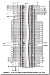
Figure 19–1 illustrates the basic outline of the Pentium II microprocessor slot 1 connector and the signals used to interface to the chip set. Figure 19–2 shows a simplified diagram of the components on the cartridge, and the placement of the Pentium II cartridge and bus components in the typical Pentium II system. There are 242 pins on the slot 1 connector for the microprocessor. (These connections are a reduction in the number of pins found on the Pentium and the Pentium II microprocessors.) The Pentium II is packaged on a printed circuit board instead of the integrated circuits of the past Intel microprocessors. The level 1 cache is 32K bytes as it was in the Pentium Pro, but the level 2 cache is no longer inside the integrated circuit. Intel changed the architecture so that a level 2 cache could be placed very close to the microprocessor. This change makes the microprocessor less expensive and still allows the level 2 cache to operate eficiently. The Pentium level 2 cache operates at one half the microprocessor clock frequency, instead of the 66 MHz of the Pentium microprocessor. A 400 MHz Pentium II has a cache speed of 200 MHz. The Pentium II is available in three versions. The first is the full-blown Pentium II, which is the Pentium II for the slot 1 connector. The second is the Celeron, which is like the Pentium II, except that the slot 1 circuit board does not contain a level 2 cache; the level 2 cache in the Celeron system is located on the main board and operates at 66 MHz. The most recent version is the Xeon, which, because it uses a level 2 cache of 512K, 1M, or 2M, represents a significant speed improvement over the Pentium II. The Xeon’s level 2 cache operates at the clock frequency of the microprocessor. A 400 MHz Xeon has a level 2 cache speed of 400 MHz, which is twice the speed of the regular Pentium II.

The early versions of the Pentium II require a 5.0 V, 3.3 V, and variable voltage power sup- ply for operation. The main variable power supply voltages vary from 3.5 V to as low as 1.8 V at the microprocessor. This is known as the core microprocessor voltage. The power-supply current averages 14.2 A to 8.4 A, depending on the operating frequency and voltage of the Pentium II. Because these currents are significant, so is the power dissipation of these microprocessors. At present, a good heat sink with considerable airflow is required to keep the Pentium II cool. Luckily, the heat sink and fan are built into the Pentium II cartridge. The latest versions of the Pentium II have been improved to reduce the power dissipation.

Each Pentium II cartridge output pin is capable of providing at least 36 mA of current at a logic 0 level on the signal connections. Some of the output control signals provide only 14 mA of current. Another change to the Pentium II is that the outputs are open-drain and require an external pull-up resister for proper operation.

The function of each Pentium II group of pins follows:

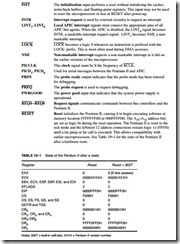
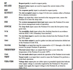
A20 Address A20 mask is an input that is asserted in the real mode to signal the Pentium II to perform address wraparound, as in the 8086 microprocessor, for use of the HIMEM.SYS driver.

The Memory System

The memory system for the Pentium II microprocessor is 64G bytes in size, just like the Pentium Pro microprocessor. Both microprocessors address a memory system that is 64 bits wide with an address bus that is 36 bits wide. Most systems use SDRAM operating at 66 MHz or 100 MHz for the Pentium II. The SDRAM for the 66 MHz system has an access time of 10 ns and the SDRAM for the 100 MHz system has an access time of 8 ns. The memory system, which connects to the chip set, is not illustrated in this chapter. Refer to earlier chapters to see the organization of a 64-bit-wide memory system without ECC.

The Pentium II memory system is divided into eight or nine banks that each store a byte of data. If the ninth byte is present, it stores an error-checking code (ECC). The Pentium II, like the 80486–Pentium Pro, employs internal parity generation and checking logic for the memory system’s data bus information. (Note that most Pentium II systems do not use parity checks, but it is available.) If parity checks are employed, each memory bank contains a ninth bit. The 64-bit- wide memory is important to double-precision floating-point data. Recall that a double-precision floating-point number is 64 bits wide. As with the Pentium Pro, the memory system is numbered in bytes from byte 000000000H to byte FFFFFFFFFH. Please note that none of the current chip sets support more than 1G byte of system memory, so the additional address connections are for

The Pentium II, Pentium III, Pentium 4,and Core2 Microprocessors-0490The Pentium II, Pentium III, Pentium 4,and Core2 Microprocessors-0491The Pentium II, Pentium III, Pentium 4,and Core2 Microprocessors-0492The Pentium II, Pentium III, Pentium 4,and Core2 Microprocessors-0493The Pentium II, Pentium III, Pentium 4,and Core2 Microprocessors-0494

The Memory System
The memory system for the Pentium II microprocessor is 64G bytes in size, just like the Pentium Pro microprocessor. Both microprocessors address a memory system that is 64 bits wide with anaddress bus that is 36 bits wide. Most systems use SDRAM operating at 66 MHz or 100 MHz
for the Pentium II. The SDRAM for the 66 MHz system has an access time of 10 ns and the SDRAM for the 100 MHz system has an access time of 8 ns. The memory system, which connects to the chip set, is not illustrated in this chapter. Refer to earlier chapters to see the organization of a 64-bit-wide memory system without ECC.
The Pentium II memory system is divided into eight or nine banks that each store a byte of data. If the ninth byte is present, it stores an error-checking code (ECC). The Pentium II, like the 80486–Pentium Pro, employs internal parity generation and checking logic for the memory system’s data bus information. (Note that most Pentium II systems do not use parity checks, but it is available.) If parity checks are employed, each memory bank contains a ninth bit. The 64-bitwide memory is important to double-precision floating-point data. Recall that a double-precision floating-point number is 64 bits wide. As with the Pentium Pro, the memory system is numbered in bytes from byte 000000000H to byte FFFFFFFFFH. Please note that none of the current chip sets support more than 1G byte of system memory, so the additional address connections are for

The Pentium II, Pentium III, Pentium 4,and Core2 Microprocessors-0495

future expansion. Figure 19–3 illustrates the basic memory map of the Pentium II system, using the AGP for the video card.

The memory map for the Pentium II system is similar to the map illustrated in earlier chapters, except that an area of the memory is used for the AGP area. The AGP area allows the video card and Windows to access the video information in a linear address space. This is unlike the 128K-byte window in the DOS area for a standard VGA video card. The benefit is much faster video updates because the video card does not need to page through the 128K-byte DOS video memory.

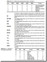
Transfers between the Pentium II and the memory system are controlled by the 440 LX or 440 BX chip set. Data transfers between the Pentium II and the chip set are eight bytes wide. The chip set communicates to the microprocessor through the five REQ signals, as listed in Table 19–3. In essence, the chip set controls the Pentium II, which is a departure from the traditional method of connecting a microprocessor to the system directly to the memory.

The Pentium II connects only directly to the cache, which is on the Pentium II cartridge. As mentioned, the Pentium II cache operates at one half the clock frequency of the micro- processor. Therefore, a 400 MHz Pentium II cache operates at 200 MHz. The Pentium II Xeon

The Pentium II, Pentium III, Pentium 4,and Core2 Microprocessors-0496

Input/Output System

The input/output system of the Pentium II is completely compatible with earlier Intel micro- processors. The I/O port number appears on address lines A15–A3 with the bank-enable signals used to select the actual memory banks used for the I/O transfer. Transfers are controlled by the chip set, which is a departure from the standard microprocessor architecture before the Pentium II.

Beginning with the 80386 microprocessor, I/O privilege information is added to the TSS segment when the Pentium II is operated in the protected mode. Recall that this allows I/O ports to be selectively inhibited. If the blocked I/O location is accessed, the Pentium II generates a type 13 interrupt to signal an I/O privilege violation.

The Pentium II, Pentium III, Pentium 4,and Core2 Microprocessors-0497

System Timing

As with any microprocessor, the system timing signals must be understood in order to interface the microprocessor, or so it was at one time. Because the Pentium II is designed to be controlled by the chip set, the timing signals between the microprocessor and the chip set have become proprietary to Intel.


QUESTIONS AND PROBLEMS ON THE PENTIUM AND PENTIUM PRO MICROPROCESSORS.

QUESTIONS AND PROBLEMS

1. How much memory is accessible to the Pentium microprocessor?

2. How much memory is accessible to the Pentium Pro microprocessor?

3. The memory data bus width is in the Pentium.

4. What is the purpose of the DP0–DP7 pins on the Pentium?

5. If the Pentium operates at 66 MHz, what frequency clock signal is applied to the CLK pin?

6. What is the purpose of the BRDY pin on the Pentium?

7. What is the purpose of the AP pin on the Pentium?

8. How much memory access time is allowed by the Pentium, without wait states, when it is operated at 66 MHz?

9. What Pentium pin is used to insert wait states into the timing?

10. A wait state is an extra clocking period.

11. Explain how two integer units allow the Pentium to execute two nondependent instructions simultaneously.

12. How many caches are found in the Pentium and what are their sizes?

13. How wide is the Pentium memory data sample window for a memory read operation?

14. Can the Pentium execute three instructions simultaneously?

15. What is the purpose of the SMI pin?

16. What is the system memory-management mode of operation for the Pentium?

17. How is the system memory-management mode exited?

18. Where does the Pentium begin to execute software for an SMI interrupt input?

19. How can the system memory-management unit dump address be modified?

20. Explain the operation of the CMPXCHG8B instruction.

21. What information is returned in register EAX after the CPUID instruction executes with an initial value of 0 in EAX?

22. What new flag bits are added to the Pentium microprocessor?

23. What new control register is added to the Pentium microprocessor?

24. Describe how the Pentium accesses 4M pages.

25. Explain how the time-stamp counter functions and how it can be used to time events.

26. Contrast the Pentium with the Pentium Pro microprocessor.

27. Where are the bank enable signals found in the Pentium Pro microprocessor?

28. How many address lines are found in the Pentium Pro system?

29. What changes have been made to CR4 in the Pentium Pro and for what purpose?

30. Compare access times in the Pentium system with the Pentium Pro system.

31. What is ECC?

32. What type of SDRAM must be purchased to use ECC?


SUMMARY OF THE PENTIUM AND PENTIUM PRO MICROPROCESSORS.

SUMMARY

1. The Pentium microprocessor is almost identical to the earlier 80386 and 80486 micro- processors. The main difference is that the Pentium has been modified internally to contain a dual cache (instruction and data) and a dual integer unit. The Pentium also operates at a higher clock speed of 66 MHz.

2. The 66 MHz Pentium requires 3.3 A of current, and the 60 MHz version requires 2.91 A. The power supply must be a +5.0 V supply with a regulation of ±5%. Newer versions of the Pentium require a 3.3 V or 2.7 V power supply.

3. The data bus on the Pentium is 64 bits wide and contains eight byte-wide memory banks selected with bank enable signals (BE7–BE0).

4. Memory access time, without wait states, is only about 18 ns in the 66 MHz Pentium. In many cases, this short access time requires wait states that are introduced by controlling the BRDY input to the Pentium.

5. The superscalar structure of the Pentium contains three independent processing units: a floating-point processor and two integer processing units labeled U and V by Intel.

6. The cache structure of the Pentium is modified to include two caches. One 8K × 8 cache is

designed as an instruction cache; the other 8K × 8 cache is a data cache. The data cache can be operated as either a write-through or a write-back cache.

7. A new mode of operation called the system memory-management (SMM) mode has been added to the Pentium. The SMM mode is accessed via the system memory-management interrupt applied to the SMI input pin. In response to SMI, the Pentium begins executing software at memory location 38000H.

8. New instructions include the CMPXCHG8B, RSM, RDMSR, WRMSR, and CPUID. The CMPXCHG8B instruction is similar to the 80486 CMPXCHG instruction. The RSM instruction returns from the system memory-management interrupt. The RDMSR and WRMSR instructions read or write to the machine-specific registers. The CPUID instruction reads the CPU identification code from the Pentium.

9. The built-in self-test (BIST) allows the Pentium to be tested when power is first applied to the system. A normal power-up reset activates the RESET input to the Pentium. A BIST power-up reset activates INIT and then deactivates the RESET pin. EAX is equal to a 00000000H in the BIST passes.

10. A new proprietary Intel modification to the paging unit allows 4M-byte memory pages instead of the 4K-byte pages. This is accomplished by using the page directory to address 1024 page tables that each contains 4M of memory.

11. The Pentium Pro is an enhanced version of the Pentium microprocessor that contains not only the level 1 caches found inside the Pentium, but also the level 2 cache of 256K or 512K found on most main boards.

12. The Pentium Pro operates by using the same 66 MHz bus speed as the Pentium and the 80486. It uses an internal clock generator to multiply the bus speed by various factors to obtain higher internal execution speeds.

13. The only significant software difference between the Pentium Pro and earlier microprocessors is the addition of the FCMOV and CMOV instructions.

14. The only hardware difference between the Pentium Pro and earlier microprocessors is the addition of 2M paging and four extra address lines that allow access to a memory address space of 64G bytes.

15. Error correction code has been added to the Pentium Pro, which corrects any single-bit error and detects any two-bit error.


THE PENTIUM AND PENTIUM PRO MICROPROCESSORS:SPECIAL PENTIUM PRO FEATURES.

SPECIAL PENTIUM PRO FEATURES

The Pentium Pro is essentially the same microprocessor as the 80386, 80486, and Pentium, except that some additional features and changes to the control register set have occurred. This section highlights the differences between the 80386 control register structure and the Pentium Pro control register.

Control Register 4

Figure 18–17 shows control register 4 of the Pentium Pro microprocessor. Notice that CR4 has two new control bits that are added to the control register array.

This section of the text explains only the two new Pentium Pro components in the control register 4. (Refer to Figure 18–8 for a description and illustration of the Pentium control registers.) Following is a description of the Pentium CR4 bits and the new Pentium Pro control bits in control register CRM4:

VME Virtual mode extension enables support for the virtual interrupt flag in protected mode. If VME = 0, virtual interrupt support is disabled.

PVI Protected mode virtual interrupt enables support for the virtual interrupt flag in protected mode.

TSD Time stamp disable controls the RDTSC instruction.

DE Debugging extension enables I/O breakpoint debugging extensions when set.

PSE Page size extension enables 4M-byte memory pages when set in the Pentium, or 2M-byte pages when set in the Pentium Pro whenever PSE is also set.

PAE Page address extension enables address lines A35–A32 whenever a special new addressing mode, controlled by PGE, is enabled for the Pentium Pro.

MCE Machine check enable enables the machine checking interrupt.

PGE Page extension controls the new, larger 64G addressing mode whenever it is set along with PAE and PSE.

The Pentium and Pentium Pro Microprocessors-0488


THE PENTIUM AND PENTIUM PRO MICROPROCESSORS:INTRODUCTION TO THE PENTIUM PRO MICROPROCESSOR.

INTRODUCTION TO THE PENTIUM PRO MICROPROCESSOR

Before this or any other microprocessor can be used in a system, the function of each pin must be understood. This section of the chapter details the operation of each pin, along with the external memory system and I/O structures of the Pentium Pro microprocessor.

The Pentium and Pentium Pro Microprocessors-0480

versions: One version contains a 256K level 2 cache; the other contains a 512K level 2 cache. The most notable difference in the pin-out of the Pentium Pro, when compared to the Pentium, is that there are provisions for a 36-bit address bus, which allows access to 64G bytes of memory. This is meant for future use because no system today contains anywhere near that amount of memory.

As with most recent versions of the Pentium microprocessor, the Pentium Pro requires a single +3.3 V or +2.7 V power supply for operation. The power supply current is a maximum of 9.9 A for the 150 MHz version of the Pentium Pro, which also has a maximum power dissipation of 26.7 W. A good heat sink with considerable airflow is required to keep the Pentium Pro cool. As with the Pentium, the Pentium Pro contains multiple VCC and VSS connections that must all be connected for proper operation. The Pentium Pro contains VCCP pins (primary VCC) that connect to +3.1 V, VCCS (secondary VCC) pins that connect to +3.3 V, and VCC5 (standard VCC) pins that connect to +5.0 V. There are some pins that are labeled N/C (no connection) and must not be connected.

Each Pentium Pro output pin is capable of providing an ample 48.0 mA of current at a logic 0 level. This represents a considerable increase in drive current, compared to the 2.0 mA available on earlier microprocessor output pins. Each input pin represents a small load, requiring only 15 μA of current. Because of the 48.0 mA of drive current available on each output, only an extremely large system requires bus buffers.

Internal Structure of the Pentium Pro

The Pentium Pro is structured differently than earlier microprocessors. Early microprocessors contained an execution unit and a bus interface unit with a small cache buffering the execution unit for the bus interface unit. This structure was modified in later microprocessors, but the modifications were just additional stages within the microprocessors. The Pentium architecture is also a modification, but more significant than earlier microprocessors. Figure 18–13 shows a block diagram of the internal structure of the Pentium Pro microprocessor.

The system buses, which communicate to the memory and I/O, connect to an internal level 2 cache that is often on the main board in most other microprocessor systems. The level 2 cache in the Pentium Pro is either 256K bytes or 512K bytes. The integration of the level 2 cache speeds processing and reduces the number of components in a system.

The bus interface unit (BIU) controls the access to the system buses through the level 2 cache, as it does in most other microprocessors. Again, the difference is that the level 2 cache is integrated. The BIU generates the memory address and control signals, and passes and fetches data or instructions to either a level 1 data cache or a level 1 instruction cache. Each cache is 8K bytes in size at present and may be made larger in future versions of the microprocessor. Earlier versions of the Intel microprocessor contained a unified cache that held both instructions and data. The implementation of separate caches improves performance because data-intensive pro- grams no longer fill the cache with data.

The instruction cache is connected to the instruction fetch and decode unit (IFDU). Although not shown, the IFDU contains three separate instruction decoders that decode three instructions simultaneously. Once decoded, the outputs of the three decoders are passed to the instruction pool, where they remain until the dispatch and execution unit or retire unit obtains them. Also included within the IFDU is a branch prediction logic section that looks ahead in code sequences that contain conditional jump instructions. If a conditional jump is located, the branch prediction logic tries to determine the next instruction in the flow of a program.

Once decoded instructions are passed to the instruction pool, they are held for processing. The instruction pool is a content-addressable memory, but Intel never states its size in the literature.

The dispatch and execute unit (DEU) retrieves decoded instructions from the instruction pool when they are complete, and then executes them. The internal structure of the DEU is

The Pentium and Pentium Pro Microprocessors-0481

illustrated in Figure 18–14. Notice that the DEU contains three instruction execution units: two for processing integer instructions and one for floating-point instructions. This means that the Pentium Pro can process two integer instructions and one floating-point instruction simultaneously. The Pentium also contains three execution units, but the architecture is different because the Pentium does not contain a jump execution unit or address generation units, as does the Pentium Pro. The reservation station (RS) can schedule up to five events for execution and process four simultaneously. Note that there are two station components connected to one of the address generation units that does not appear in the illustration of Figure 18–14.

The last internal structure of the Pentium Pro is the retire unit (RU). The RU checks the instruction pool and removes decoded instructions that have been executed. The RU can remove three decoded instructions per clock pulse.

The Pentium and Pentium Pro Microprocessors-0482

Pin Connections

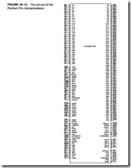
The number of pins on the Pentium Pro has increased from the 237 pins on the Pentium to 387 pins on the Pentium Pro. Following is a description of each pin or grouping of pins:

A20M

clip_image007clip_image007[1]clip_image008clip_image009clip_image010A35–A3 ADS AP1, AP0

clip_image011clip_image011[1]ASZ1, ASZ0

The address A20 mask is an input that is asserted in the real mode to signal the Pentium Pro to perform address wraparound, as in the 8086 microproces- sor, for use of the HIMEM.SYS driver.

Address bus connections address any of the 8G × 64 memory locations found in the Pentium Pro memory system.

The address data strobe becomes active whenever the Pentium Pro has issued a valid memory or I/O address.

Address parity provides even parity for the memory address on all Pentium Pro–initiated memory and I/O transfers. The AP0 output provides parity for address connections A23–A3, and the AP1 output provides parity for address connections A35–A24.

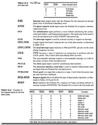
Address size inputs are driven to select the size of the memory access. Table 18–6 illustrates the size of the memory access for the binary bit patterns on these two inputs to the Pentium Pro.

BCLK The bus clock input determines the operating frequency of the Pentium Pro microprocessor. For example, if BCLK is 66 MHz, various internal clocking speeds are selected by the logic levels applied to the pins in Table 18–7. A BCLK frequency of 66 MHz runs the system bus at 66 MHz.

BERR

The bus error input/output either signals a bus error along or is asserted by an external device to cause a machine check interrupt or a non-maskable interrupt.

The Pentium and Pentium Pro Microprocessors-0483The Pentium and Pentium Pro Microprocessors-0484

The Pentium and Pentium Pro Microprocessors-0485The Pentium and Pentium Pro Microprocessors-0486

The Memory System

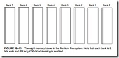
The memory system for the Pentium Pro microprocessor is 4G bytes in size, just as in the 80386DX–Pentium microprocessors, but access to an area between 4G and 64G is made possible by additional address signals A32–A35. The Pentium Pro uses a 64-bit data bus to address memory organized in eight banks that each contain 8G bytes of data. Note that the additional memory is enabled with bit position 5 of CR4 and is accessible only when 2M paging is enabled. Note also that 2M paging is new to the Pentium Pro to allow memory above 4G to be accessed. More information is presented on Pentium Pro paging later in this chapter. Refer to Figure 18–15 for the organization of the Pentium Pro physical memory system.

The Pentium Pro memory system is divided into eight banks where each bank stores a byte-wide data with a parity bit. Note that most Pentium and Pentium Pro microprocessor-based systems forgo the use of the parity bit. The Pentium Pro, like the 80486 and Pentium, employs internal parity generation and checking logic for the memory system data bus information. The 64-bit-wide memory is important to double-precision floating-point data. Recall that a double- precision floating-point number is 64 bits wide. As with earlier Intel microprocessors, the memory system is numbered in bytes from byte 000000000H to byte FFFFFFFFFH. This nine-digit hexadecimal address is employed in a system that addresses 64G of memory.

Memory selection is accomplished with the bank enable signals (BE7–BE0). In the Pentium Pro microprocessor, the bank enable signals are presented on the address bus (A15–A8) during the second clock cycle of a memory or I/O access. These must be extracted from the address bus to access memory banks. The separate memory banks allow the Pentium Pro to access any single byte, word, doubleword, or quadword with one memory transfer cycle. As with earlier memory selection logic, we often generate eight separate write strobes for writing to the memory system. Note that the memory write information is provided on the request lines from the microprocessor during the second clock phase of a memory or I/O access.

A new feature added to the Pentium and Pentium Pro is the capability to check and generate parity for the address bus during certain operations. The AP pin (Pentium) or pins (Pentium Pro) provide the system with parity information, and the APCHK (Pentium) or AP pins (Pentium Pro) indicate a bad parity check for the address bus. The Pentium Pro takes no action when an address-parity error is detected. The error must be assessed by the system, and the system must take appropriate action (an interrupt) if so desired.

New to the Pentium Pro is a built-in error-correction circuit (ECC) that allows the correction of a one-bit error and the detection of a two-bit error. To accomplish the detection and

The Pentium and Pentium Pro Microprocessors-0487

correction of errors, the memory system must have room for an extra 8-bit number that is stored with each 64-bit number. The extra 8 bits are used to store an error-correction code that allows the Pentium Pro to automatically correct any single-bit error. A 1M × 64 is a 64M SDRAM without ECC, and a 1M × 72 is an SDRAM with EEC support. The ECC code is much more reliable than the old parity scheme, which is rarely used in modern systems. The only drawback of the ECC scheme is the additional cost of SDRAM that is 72 bits wide.

Input/Output System

The input/output system of the Pentium Pro is completely compatible with earlier Intel micro- processors. The I/O port number appears on address lines A15–A3 with the bank enable signals used to select the actual memory banks used for the I/O transfer.

System Timing

As with any microprocessor, the system timing signals must be understood in order to interface the microprocessor. This portion of the text details the operation of the Pentium Pro through its timing diagrams and shows how to determine memory access times.

The basic Pentium Pro memory cycle consists of two sections: the address phase and the data phase. During the address phase, the Pentium Pro sends the address (T1) to the memory and I/O system, and also the control signals (T2). The control signals include the ATTR lines (A31–A24), the DID lines (A23–A16), the bank enable signals (A15–A8), and the EXF lines (A7–A3). See Figure 18–16 for the basic timing cycle. The type of memory cycle appears on the request pins. During the data phase, four 64-bit-wide numbers are fetched or written to the memory. This operation is most common because data from the main memory are transferred between the internal 256K or 512K write-back cache and the memory system. Operations that write a byte, word, or doubleword, such as I/O transfers, use the bank selection signals and have only one clock in the data transfer phase. Notice from the timing diagram that the 66 MHz Pentium Pro is capable of 33 million memory transfers per second. (This assumes that the memory can operate at that speed.)

The setup time before the clock is given as 5.0 ns and the hold time after the clock is given as 1.5 ns. This means that the data window around the clock is 6.5 ns. The address appears on the ns maximum after the start of T1. This means that the Pentium Pro microprocessor operating at 66 MHz allows 30 ns (two clocking periods), minus the address delay time of 8.0 ns and also


THE PENTIUM AND PENTIUM PRO MICROPROCESSORS:NEW PENTIUM INSTRUCTIONS.

NEW PENTIUM INSTRUCTIONS

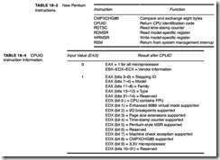
The Pentium contains only one new instruction that functions with normal system software; the remainder of the new instructions are added to control the memory-management mode feature and serializing instructions. Table 18–3 lists the new instructions added to the Pentium instruction set.

The CMPXCHG8B instruction is an extension of the CMPXCHG instruction added to the 80486 instruction set. The CMPXCHG8B instruction compares the 64-bit number stored in EDX and EAX with the contents of a 64-bit memory location or register pair. For example, the CMPXCHG8B DATA2 instruction compared the eight bytes stored in memory location DATA2 with the 64-bit number in EDX and EAX. If DATA2 equals EDX:EAX, the 64-bit number stored in ECX:EBX is stored in memory location DATA2. If they are not equal, the contents of DATA2 are stored into EDX:EAX. Note that the zero flag bit indicates that the contents of EDX:EAX were equal or not equal to DATA2.

The CPUID instruction reads the CPU identification code and other information from the Pentium. Table 18–4 shows different information returned from the CPUID instruction for various input values for EAX. To use the CPUID instruction, first load EAX with the input value and then execute CPUID. The information is returned in the registers indicated in the table.

The Pentium and Pentium Pro Microprocessors-0475

If a 0 is placed in EAX before executing the CPUID instruction, the microprocessor returns the vendor identification in EBX, EDX, and EBX. For example, the Intel Pentium returns “GenuineIntel” in ASCII code with the “Genu” in the EBX, “ineI’ in EDX, and “ntel” in ECX. The EDX register returns information if EAX is loaded with a 1 before executing the CPUID instruction.

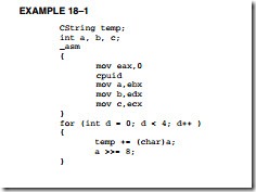
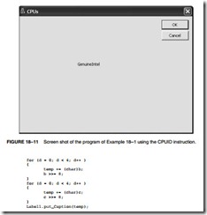
Example 18-1 illustrates a short program that reads the vendor information with the CPUID instruction. This software was placed into the TODO: section of the OnInitDialog function of a simple dialog application. It then displays it on the video screen in an ActiveX label as illustrated in Figure 18–11. The CPUID instruction functions in both the real and protected mode and can be used in any Windows application.

The Pentium and Pentium Pro Microprocessors-0476The Pentium and Pentium Pro Microprocessors-0477

The RDTSC instruction reads the time-stamp counter into EDX:EAX. The time-stamp counter counts CPU clocks from the time the microprocessor is reset, where the time-stamp counter is initialized to an unknown count. Because this is a 64-bit count, a 1GHz microproces- sor can accumulate a count of over 580 years before the time-stamp counter rolls over. This instruction functions only in real mode or privilege level 0 in protected mode.

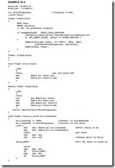
Example 18-2 shows a class written for Windows that provides member functions for accurate time delays and also member functions to measure software execution times. This class is added by right-clicking on the project name and inserting an MFC generic class named TimeD. It contains three member functions called Start, Stop, and Delay.The Start( ) function is used to start a measurement and Stop( ) is used to end a time measurement. The Stop( ) function returns a double floating-point value that is the amount of time in microseconds between Start( ) and Stop( ).

The Delay function causes a precision time delay based on the time-stamp counter. The parameter transferred to the Delay function is in milliseconds. This means that a Delay(1000) causes exactly 1000 ms of delay.

When TimeD is initialized in a program, it reads the microprocessor frequency in MHz from the Windows registry file using the RegQueryValueEx function after opening it with the RegOpenKeyEx function. The microprocessor clock frequency is returned in the MicroFrequency class variable.

The Pentium and Pentium Pro Microprocessors-0478

If an additional Delay is needed, it could be added to the class to cause delays in microseconds, but a restriction should be made so it is no less than about 2 or 3 microseconds, because of the time that it takes to add the time to the count from the time-stamp counter.

Example 18-3 shows a sample dialog application that used Delay( ) to wait for a second after clicking the button before changing the foreground color of an ActiveX Label. What does not appear in the example is that at the beginning of the dialog class an #include “TimeD.h” statement appears. The software itself is in the TODO: section of the OnInitDialog function.

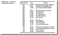
The RDMSR and WRMSR instructions allow the model-specific registers to be read or written. The model-specific registers are unique to the Pentium and are used to trace, check performance, test, and check for machine errors. Both instructions use ECX to convey the register number to the microprocessor and use EDX:EAX for the 64-bit-wide read or write. Note that the register addresses are 0H–13H. See Table 18–5 for a list of the Pentium model-specific registers and their contents. As with the RDTSC instruction, these model-specific registers operate in the real or privilege level 0 of protected mode.

Never use an undefined value in ECX before using the RDMSR or WRMSR instructions. If ECX = 0 before the read or write machine-specific register instruction, the value returned, EDX:EAX, is the machine check exception address. (EDX:EAX is where all data reside when written or read from the model-specific registers.) If ECX = 1, the value is the machine check exception type; if ECX = 0EH, the test register 12 (TR12) is accessed. Note that these are internal registers designed for in-house testing. The contents of these registers are proprietary to Intel and should not be used during normal programming.

The Pentium and Pentium Pro Microprocessors-0479