IC BUFFER

IC BUFFER

Context

● You are developing an embedded application using one or more members of the 8051 family of microcontrollers.

● You are designing an appropriate hardware foundation for your application.

Problem

How do you safely control one or more small, low-power DC loads from a single microcontroller port?

Background

Suppose we try to control eight 10 mA LEDs from a single port using the techniques discussed in NAKED LED [page 110]. Figure 7.8 illustrates one way in which we might try to achieve this.

In almost all circumstances, this approach will fail. As discussed in NAKED LED , the various members of the 8051 family can typically sink or source around 10 mA of cur- rent per port pin. This figure does not, however, give the whole story. Take one family member as an example. The Atmel 89C52 is a modern ‘standard’ 8051 device (40 pins, 4 ports), which is used in various examples throughout this book. It can sink up to 10 mA per port pin. However, in total, P0 can sink only 26 mA (over all port pins) and P1, P2 and P3 can only each sink a total of 15 mA. Overall, at most, the whole chip can sink only 71 mA.

Driving DC Loads-0127

[Note: IN MOST CASES, UNLESS YOU USE LOW-CURRENT (~1 mA) LEDs, THIS WILL DESTROY THE PORT (and often the microcontroller too). ]

Although the various 8051 family members vary, these figures are representative of those found in many devices. As a result, circuits like that shown in Figure 7.8 – which require a total current flow of around 80 mA for typical LEDs – cannot generally be used.

Solution

As discussed in ‘Background’, buffers can be needed if we need to drive multiple low- power loads from one microcontroller. Even where the ports can drive loads directly, we can both reduce the risk of damage to the ports and safeguard the application as a whole by using an IC buffer between the microcomputer and the load.

We consider, first, some of the many ICs that may be used as buffers and, second, the need for pull-up resistors at the buffer outputs.

Finding an IC

Various ICs can be used as buffers in this way. Suitable inverters are readily and very cheaply available: six are packaged together, for example, in the ubiquitous 74×04 (Figure 7.9).

An alternative to the 74×04 is the inverting (74×240) and non-inverting (74×241) buffers that come in packages of eight (see Figures 7.10 and 7.11). These are particu- larly useful when buffering a whole port.

Driving DC Loads-0128

[Note: that each chip contains eight buffers, arranged in two groups of four (Group 1, Group 2). The buffers are all tri-state devices and, for use as a simple buffer, the gates must be enabled (in the case of Group 1) by applying a low (~0V) input to Gate 1 or (in the case of Group 2) Gate 2. ]

Driving DC Loads-0129

[Note: that, like the 240, each chip contains eight buffers, arranged in two groups of 4 (Group 1, Group 2). The buffers are all tri-state devices and, for use as a simple buffer, the gates must be enabled (in the case of Group 1) by applying a low (~0V) input to Gate 1, or (in the case of Group 2), by applying a high (~5V) input to Gate 2.]

Note that these buffers are all members of the ‘74’ series of ICs. All these 74x buffers can handle currents of 20 mA per pin. The total current per device is 70 mA in the case of the 240/241/244 devices and 50 mA for the 04. If your load satisfies the 20 mA per pin requirement but not the ‘per device’ requirement, you will need to use more than one buffer chip.

All these buffers operate reasonably rapidly, with a maximum delay of about 1 µs.

Logic families

The various ‘74’ series buffers just described are available in numerous versions, including ‘LS’ (the 74LS04 etc.), ‘ALS’, ‘HC’, HCT, VHCT, AHC, AHCT and so on. The different versions have different switching speeds, power consumption, operating voltages and prices. In general, you can choose any buffer that matches the needs of your project.

Despite the vast range of ‘74’ buffers available there are only two logic families: CMOS and TTL. The CMOS devices generally have a ‘C’ somewhere in the name (e.g. 74HC04) while the TTL devices generally have an ‘S’ somewhere in the name (e.g. 74ALS04). You need to be aware of the differences between these two families.

The original 5V TTL family dates from around 1964. It has undergone various improvements and is still widely used. Its main advantage is that it is fast; its main disadvantage is that it has comparatively high power consumption figures.

The main competitor to TTL is the CMOS family. The 5V CMOS dates back to around 1983 and it too has undergone various improvements. Its main advantage is low power consumption and – in recent devices – speed has been greatly improved. It seems likely that CMOS logic families will come to replace TTL logic over the next few years.

Any 8051 microcontroller can drive a buffer made from TTL or CMOS logic with- out difficulty. However, there are differences in the buffer outputs depending on the technology used; these differences are important:

● With (5V) TTL, the Logic 0 output is in the range 0 to 1.5V; the Logic 1 output is 3.5 to 5V.

● With (5V) CMOS, the Logic 0 output is ~0V; the Logic 1 output is ~5V.

These differences have significant implications. For example, consider that we wish to use a CMOS logic gate to buffer an LED output (Figure 7.12). This approach works very effectively, because of the large, fixed voltage swing; however, consider the same buffer implemented using a TTL buffer (Figure 7.13).

In Figure 7.13 we show that the TTL buffer has two disadvantages. First, we need a pull-up resistor (the usual 5K–10K value) to pull the ‘high’ output to 5V. Second, the ‘low’ output varies, in a range from 0 to 1.5V. This makes it very difficult to choose an appropriate value of resistor to ensure that we have a bright display and – at the same time – do not exceed the buffer or LED current capacity.

Driving DC Loads-0130

Use CMOS buffers

As these discussions suggest, it makes sense to use CMOS logic in your buffer designs wherever possible. You should also make it clear in the design documenta- tion that CMOS logic is to be used.

If working with boards designed by other people, the use of pull-up resistors at the buffer outputs can suggest that TTL logic was assumed; however, CMOS logic can still be used. If there is no pull-up resistor, then CMOS should be used.

Using pull-up resistors at the buffer inputs

As usual, if working with port pins that do not have internal pull-up resistors, you need to include such resistors (10K will do) at the input to the IC buffer, whatever kind of logic you are using.

See NAKED LED [page 110] for further details.

Hardware resource implications

Every implementation of this pattern uses at least one port pin.

Reliability and safety implications

A key design decision to be made when driving a small output device is whether or not to use a buffer.

In some circumstances, omitting the buffer can make your system potentially less safe. For example, if you have an LED accessible at the front of an embedded applica- tion, someone wishing to interfere with the system may try to apply a high voltage across this LED or to damage it physically. If the LED is connected directly to a port pin, then it may be possible to damage the microcontroller itself through damage to the LED: if there is a suitable buffer between the LED and the microcontroller, it is much less likely that any damage to the microcontroller will be possible.

Use of a buffer will increase production costs. However, if there is any possibility of the output device suffering damage while the product is in use, a buffer may be a good option: it is almost always cheaper to replace a blown buffer (~$0.10) than it is to replace a blown microcontroller (~$1.00+). As a result, for low-volume and / or high-cost products where repairs may be required, then buffers are a good solution.

Overall, if reliability is an issue, use a buffer. Otherwise, in very low-cost (or high- volume) products, or in situations where repair is not a practical proposition, then use of a buffer will simply add to production costs.

Portability

These techniques work with all 8051s (and most other microcontroller and micro- processor families).

As usual, if working with port pins that do not have internal pull-up resistors, you need to include such resistors (10K will do) in your design: see NAKED LED [page 110] for further details.

Overall strengths and weaknesses

IC buffers allow multiple (small) loads to be controlled from a single port. Buffers can improve reliability.

Use of buffers increases the product cost.

Related patterns and alternative solutions

The other patterns in this chapter (particularly IC DRIVER [page 134]) provide alternative solutions.

Example: Buffering three LEDs with a 74HC04

Figure 7.14 shows a 74HC04 buffering three LEDs. As discussed in ‘Solution’, we do not require pull-up resistors with the HC (CMOS) buffers.

In this case, we assume that these LEDs are to be driven at 15 mA each, which is within the capabilities (50 mA total) of the buffer.

The required resistor values are:

Driving DC Loads-0131


NAKED LED

NAKED LED

Context

● You are developing an embedded application using one or more members of the 8051 family of microcontrollers.

● You are designing an appropriate hardware foundation for your application.

Problem

What is the cheapest way of driving a small number of LEDs with a microcontroller?

Background

Even in the most basic application, the presence of a constant red or green output from a light-emitting diode (LED) is reassuring, implying that the application is at least powered. In other applications requiring numerical outputs, LEDs are grouped into seven- or eight-segment combinations12 to display, for example, the current time, the voltage or the number of calls received by a telephone answering machine (‘voice mail’) system. Overall, LEDs are the most widely used components in user interfaces for embedded systems.

Given the name it is hardly surprising that, electrically, an individual LED operates as a diode. LEDs have a forward voltage drop of about 2V, and typically require a cur- rent of around 5–15 mA for a bright display (Figure 7.1). Note that the forward voltage required to ‘switch on’ a conventional (silicon) diode is around 0.7 V: the dif- ference arises because LEDs are generally manufactured from gallium arsenide phosphide (see Horowitz and Hill, 1989, for further details).

Solution

The focus in this pattern is on low-cost techniques for driving LEDs.

Driving DC Loads-0119

12. Multi-segment LEDs are considered in MX LED DISPLAY [page 450].

Driving single LEDs

It is possible to drive small single LEDs directly from the port pins, as illustrated in Figure 7.2. Note that we usually need a resistor in series with the LED, between the supply and the port pin. This resistor is required to limit the current flow to the port when the LED is ‘switched on’.

To understand why this resistor is necessary, you need to remember that – as we discussed in ‘Background’ – the voltage drop across the LED will be around 2V. Assuming Vcc is 5V, then the voltage drop across the resistor and diode, when the port pin is at 0V, will be around 5V. Thus, the voltage drop across the resistor needs to be 3V. If there is no resistor, then we need to drop 3V across a stretch of wire: this can cause a very strong current to flow (limited only by the supply capacity), which will almost instantly destroy the port, the LED and, possibly, the whole microcontroller.

The equation in Figure 7.2 (essentially Ohm’s law) shows how to calculate the required resistor (R) value. Typical values of the required parameters are as follows:

● Supply voltage, Vcc = 5V

● LED forward voltage, Vdiode = 2V

● Required diode current, Idiode = 10 mA (note that the data sheet for your chosen LED will provide this information) This gives a required R value of 300Ω.

Use of pull-up resistors

Throughout this chapter, we will present examples of driver circuits like that shown in Figure 7.2.

This circuit will only work on port pins where the microcontroller has an internal pull-up resistor: this applies to most ports on the 8051 family, with the exception of Port 0. In addition, some other members of the 8051 family – notably the Atmel 89Cx051 devices – have small numbers of pins without internal pull-ups.

Driving DC Loads-0120

[Note: When calculating the required value of Rled, the resistance values are in ohms, voltages in volts and current in amps.]

To adapt circuits such as that shown in Figure 7.2 for use on pins without internal pull-up resistors is straightforward: you simply need to add an external pull-up resis- tor, as illustrated in Figure 7.3. The value of the pull-up resistor should be between 1K and 10K. This requirement applies to all of the examples in this book.

In the unlikely event that you do not know whether a drive circuit will be used on a port with pull-up resistors, the best solution is to include 10K resistors in your cir- cuit. If the port pin used already contains pull-ups, the extra resistor will have no discernible impact on the operation of the circuit.

Driving DC Loads-0121

Hardware resource implications

Every implementation of this pattern uses at least one port pin.

Reliability and safety implications

There are several reliability implications involved in the use of this pattern.

Connecting up LEDs

If you connect ordinary LEDs to a port, do not omit the resistor! The resulting high current flows may not cause the system to fail immediately, but will greatly reduce the life of the port pin and, potentially, the whole processor.

Note: There are ‘5V’ LEDs available, at higher cost: these include series resistors. Provided they have suitable current requirements, they may be safely connected directly to the port pins.

Should you use a buffer?

Where more than two LEDs are connected to a single port, buffering is almost always essential, because – while the limit for an individual port pin may be (say) 10 mA – the port as a whole may have a limit of 20 mA or less. This issue is discussed in IC BUFFER [page 118].

Use of LEDs as warning devices

LEDs (particularly flashing LEDs) are frequently used as warning devices. Bear in mind that in bright sunlight, such warnings will be barely visible and that blind or partially sighted people will never be able to see them. Adding an additional or alternative audible output may be appropriate in some systems.

General use of LEDs

LEDs consume large amounts of power (compared, for example, to liquid crystal displays) and need to be used with care in many battery-powered designs.

Portability

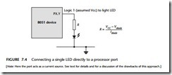
The circuits presented here can be used with almost all microcontrollers and micro- processors. Please note, however, that most of the circuits we present for driving DC and AC loads involve some form of current ‘sink’, as in Figure 7.2. Here, the current flows ‘in to’ the processor port. This is despite the fact that most microcontroller ports, manufactured using some form of MOS technology, can also ‘source’ current, so that the load could be arranged as illustrated in Figure 7.4.

However, some of the other circuits used as buffers or drivers may use different manufacturing processes, including TTL technology. TTL devices can sink current in much the same way as MOS devices, but are poor current sources. As a result, hard- ware designs based on current sinking are generally more portable (across different logic families) than designs based on current sourcing and, for this reason, will be used throughout this pattern collection.

Driving DC Loads-0122

[Note: Here the port acts as a current source. See text for details and for a discussion of the drawbacks of this approach.]

Overall strengths and weaknesses

This pattern allows small numbers of LEDs to be driven from a microcon- troller port with a minimum of external hardware.

This is a low-cost solution.

Only applicable for small numbers of LEDs (typically two per port), otherwise a buffer will be required: see IC BUFFER [page 118].

Related patterns and alternative solutions

See PORT I / O [page 174] for software details.

See the remaining patterns in this chapter for techniques suitable for driving higher powered loads.

Example: Using low-current LEDs

To emphasize that all rules can be broken, we will consider in this example how you can connect eight ‘naked’ LEDs to the port of an 8051 microcontroller without using a buffer (see Figure 7.5).

Of course, for the reasons outlined in this pattern, it is not possible to connect up ‘normal’ (~10 mA) LEDs in this way without exceeding the current capacity of the port: however, if we use low-current (2 mA) LEDs, then – with most 8051 microcon- trollers – this is possible.

Driving DC Loads-0123

Further reading

Horowitz, P. and Hill, W. (1989) The Art of Electronics, 2nd edn, Cambridge University Press, Cambridge, UK.


NAKED LOAD

NAKED LOAD

Context

● You are developing an embedded application using one or more members of the 8051 family of microcontrollers.

● You are designing an appropriate hardware foundation for your application.

Problem

How do you connect a piece of low-voltage (≤ 5V), low-power (≤ 100 mW) DC equip- ment to one of the port pins on your (8051-based) application?

Background

See NAKED LED [page 110] for general background material.

Solution

In NAKED LED [page 110] we considered how to connect an LED to a port pin of an 8051 microcontroller. In this pattern we consider a more general situation where we wish to control any small DC ‘load’ (Figure 7.6).

This shows a general (unspecified) load connected to the port pin.

The main difference between the general load and the LED is that the required voltage drop across the load will (typically) be 5V (in a 5V system: 3V in a 3V system),

Driving DC Loads-0124

rather than the 2V seen in the case of LEDs. In these circumstances, the resistor may be omitted, since the required resistance value will be:

Driving DC Loads-0125

Hardware resource implications

Every implementation of this pattern uses at least one port pin.

Reliability and safety implications

IC BUFFER [page 107] discusses techniques for buffering LEDs and other small loads. This can increase the reliability of some applications.

Portability

All microcontrollers can control small loads in this way.

Overall strengths and weaknesses

The techniques discussed in this pattern allow small loads to be driven from a microcontroller port with a minimum of external hardware.

This is a low-cost solution.

Only applicable for small loads (and small numbers of very small loads), other- wise a buffer will be required: see IC BUFFER [page 118].

Related patterns and alternative solutions

See PORT I / O [page 174] for software details.

See the pattern IC BUFFER [page 118] for techniques suitable for driving two or more small loads from a single microcontroller.

See the patterns BJT DRIVER [page 124], IC DRIVER [page 134] and MOSFET DRIVER

[page 139] for techniques suitable for driving higher powered DC loads.

Example: Buzzer

A range of piezoelectric buzzers are available that generate very loud (~70 dB) tones at microcontroller port voltages (they will operate from 3V to 12V) and currents (they require around 3 mA). These make excellent warning devices, even in battery- powered applications (see Figure 7.7).

As we discussed in ‘Solution’, this 5V load requires no series resistor.

Driving DC Loads-0126

Further reading

Horowitz, P. and Hill, W. (1989) The Art of Electronics, 2nd edn, Cambridge University Press, Cambridge, UK.


OFF-CHIP CODE MEMORY

OFF-CHIP CODE MEMORY

Context

● You are developing an embedded application using one or more members of the 8051 family of microcontrollers.

● You are designing an appropriate hardware foundation for your application.

Problem

How do you add up to 64 kbytes of external code memory (usually ROM) to your 8051 microcontroller?

Background

See OFF CHIP DA T A MEMOR Y [page 94] for background information.

Solution

If you have decided that you need to use external code memory doing so is straight- forward. Figure 6.6 illustrates the basic circuit.

The recommended latch and (ROM) memory combinations for a wide range of clock speeds are given in Table 6.3. These are taken from Dallas Application Note 89. As we noted in OFF CHIP DA T A MEMOR Y [page 94], latch and memory combinations which will operate with these Dallas devices will also work with most other (generally slower) 8051 devices.

Memory issues-0113

Memory issues-0114

[Note that, if the microcontroller is not a CMOS device and the memory devices are CMOS devices, you will require pull-up resistors (not shown) on Port 0. This is most easily achieved using a DIL (or similar) 10K resistor pack. Note also the control of the EA pin, to force the microcontroller to retrieve instructions from external memory.]

Hardware resource implications

As discussed in OFF CHIP DA T A MEMOR Y [page 94], use of external memory has major resource implications: it requires the use of two ports (P0 and P2), plus two pins (P3.6, P3.7) on Port 3. This reduces the number of available port pins from 32 to 14. See the following for additional comments on this.

Reliability and safety implications

As discussed in ON CHIP MEMOR Y [page 82], the addition of external memory can reduce the reliability of your application: use an on-chip solution where possible.

In many cases, adding external ROM can be avoided if you use an appropriate 8051-device with on-chip ROM: see ‘Related patterns and alternative solutions’ for further details.

Portability

Hardware designs for external memory are generally portable. However, if you upgrade from a ‘slow’ to a ‘fast’ processor (or simply increase the crystal frequency) you need to make sure that the external latch and memory components are suffi- ciently fast: refer to Table 6.3 for suggestions.

The only way to make your external access design as portable as possible is always to use the fastest external components available. This approach has cost implications, but, if you are able to produce 100,000 copies of one, generic (fast) board rather than smaller numbers of ‘slow’, ‘medium’ and ‘fast’ versions, you may find the ‘one size fits all’ solution to be both a reliable and cost-effective solution.

Overall strengths and weaknesses

If at all possible, use of internal code memory is a better option!

Related patterns and alternative solutions

Before you add ROM to your 8051-based system, think carefully. There are many 8051 devices with large amounts of on-chip code memory available. As an example, Table

6.4 shows a selection of recent Philips 8051 devices.

As is clear from the table, 8051 devices are now available with large amounts of on-chip ROM (and good performance levels). Of course, similar devices are available from other manufacturers.

There are, perhaps, three main reasons for adding external code memory:

● You need particular on-chip hardware components (e.g. CAN bus, ADC, hardware maths) and cannot find an 8051 device that has both sufficient ROM and the required peripheral(s).

Memory issues-0115

● You require external RAM. Having therefore already created much of the required external memory interface, you have decided that it makes good economic sense to add external ROM too, rather than using a device with on-chip ROM.

● You need to be able to update the code that your system will execute. For example, if your system is running on a comparatively expensive (Extended) 8051 device, you may decide that it will be more cost effective to replace a small ROM chip when code updates are required, rather than to replace the microcontroller itself.

Example: Adding ROM and RAM memory

Figure 6.7 illustrates how you can add both code and data memory to your system.

Example: Reducing the component count

If space is very tight and / or you are seeking to improve the reliability of your 8051- based system by keeping the number of connections to a minimum, you have two basic choices:

● Use a microcontroller with on-chip code memory.

● Use a memory (ROM) chip that does not require a latch.

Option 1 is not always available. For example, the powerful C509 microcontroller is very fast and has several useful features (including a hardware maths unit compati- ble with that in the 80C517). It does not, however, have on-chip ROM of any kind.

Memory issues-0116

To add external memory without requiring the use of a latch, consider using an Atmel AT27C520 (64 kbyte) EPROM. It has an internal latch, so no additional compo- nents are required.

Example: Adding more than 64 kbytes of code memory

With some recent exceptions (see Table 6.1), the various members of the 8051 family only directly support a maximum of 64 kbytes of external code memory. This may not be sufficient for larger programs or where large amounts of read-only variables need to be used. ‘Bank switching’ is one option.

The idea of a bank-switched memory arrangement is, superficially, very straight- forward. In a simplified arrangement, we may have (for example) eight 64-kbyte banks of memory in the system. Access to memory locations within each block is controlled by the usual (16) address lines. To select between these eight memory blocks, we can use eight additional output pins on the microcontroller to select an appropriate memory bank, as required.

In practice, things become slightly more complicated.

First, consider interrupts. When an interrupt occurs, the microcontroller will jump to a particular address in the current bank. One way of ensuring that this address contains the relevant instructions is to duplicate your interrupt functions in all the banks (note that your compiler can usually do this automatically, as we will see later).

Similarly, library functions also need to be universally accessible and, therefore, (usually) in a common area.

The need for duplication can also arise with read-only variables stored in the code area. Unless you can ensure that these constants will only be called in a particular bank, they need to be placed in a common area.

Finally, the bank-switching code itself must be in a common area.

Having addressed these problems, you need to consider what happens when the chip is reset. At this time, all port outputs are set to 0xFFFF. If a port is being used for bank switching, the port outputs will control which bank of code your program begins to execute first. You need to ensure, mainly through the bank-switching hard- ware, that your program begins by executing code in the correct bank.

Health warning!

As these comments should begin to make clear, bank switching is complicated and prone to error. Even if you know what you are doing, people who subsequently have to maintain the system you create may not fully understand the consequences of any changes they make to the code.

If possible, avoid bank switching. If your application requires more than 64 kbytes of code memory, a much better solution is to use a Dallas 80C390, Analog Devices ADµC812 or Philips 8051MX, all of which support more than 64 kbytes of code memory. Alternatively, consider one of the two ‘upgrade’ paths from the 8051 (viz, the 80251, the 8051XA) discussed in Chapter 3.

If you are determined to implement bank switching, you need, first, an appropriate address decoding scheme and, second, a means of implementing a common code area.

There are two basic ways of tackling the ‘common area’ problem. The simplest approach is simply to duplicate all the common code in every code bank. For exam- ple, Figure 6.8 shows the use of four 64-kbyte ROM chips, with a common area (around 32 kbyte) duplicated in each.

Alternatively, we can achieve a similar result by using five 32-kbyte memory devices, arranged with one common area and four upper code banks (Figure 6.9).

While superficially more efficient, the lower cost of large memory chips means that a solution based on one memory chip is most likely to prove cost effective. In addi- tion, because most of the code examples presented in this book make comparatively little use of interrupts, or of library functions, the common area required is often small in size (typically a few kbytes) and the ‘duplicated common area’ solution is therefore less inefficient than it might initially appear.

For example, consider that we wish to add a 512-kbyte ROM and 64-kbyte RAM to a C509 microcontroller. Much of the required hardware is familiar: we have an exter- nal ROM device and an external RAM device, connected to the microcontroller through an 74HC573 latch. This is exactly the same arrangement seen previously in Figure 6.7.

Memory issues-0117

Where the hardware differs is first, of course, in the size of the code memory area and, second, the presence of the 74HC257. The 74HC257 is a (quad) 2-line to 1-line data multiplexer: it provides the necessary ‘glue logic’, to interface the port pins (lower nybble of Port 3 in this example: any available port may be used).

Details of the 74HC257 connection are given in Figures 6.10 and 6.11.

Note that the Keil compiler provides support for bank switching and will support the memory arrangement shown here: see the Banker / Linker manual for details.

Memory issues-0118


Driving DC Loads

Introduction

The port pins on a typical microcontroller can be set at values of either 0V or 5V (or, in a 3V system, 0V and 3V) under software control. Each pin can typically sink (or source) a current of around 10 mA. In this chapter, we are concerned with hardware designs that will allow us to control a range of low- and high-power, direct current (DC) loads via these pins.

With care, the port may be used directly to drive low-power DC loads, such as LEDs (see NAKED LED [page 110]) or, for example, small warning buzzers (see NAKED LOAD [page 115]). However, while a limited number of such loads may be connected directly to the port, connecting, say, eight LEDs will generally exceed the total port or microcontroller capacity. In these circumstances, use of an IC-based buffer circuit can be a cost-effective solution: see IC BUFFER [page 118]. Indeed, even with small loads, the reliability of the application may be improved through the use of such a buffer.

Of course, many output devices require a higher voltage and a far greater power output than the naked ports can provide. For example, to drive even a small DC motor may require up to 1A of current at 12V. To control such devices, we need to provide appropriate driver (or interface) circuit to convert the microcontroller output to an appropriate level. We will consider three ways of driving such loads in this chapter:

● Using bipolar-junction transistors (see BJT DRIVER [page 124])

● Using a driver IC (see IC DRIVER [page 134])

● Using ‘metal oxide silicon field effect transistors’ (see MOSFET DRIVER [page 139])

Please note that in this chapter our concern will be with hardware details of the interface only. In PORT I / O [page 174] we consider software suitable for controlling such hardware.


Designing embedded systems using patterns:Limitations of existing software design techniques

Limitations of existing software design techniques

We begin the main part of this chapter by considering two examples which illustrate the limitations of standard design techniques when used for embedded system development.

Cruise-control system

As a first example, we will consider a cruise-control system (CCS) for a road vehicle. A CCS is often used to demonstrate the effectiveness of real-time software design methodologies (for example, see Hatley and Pirbhai, 1987; Awad et al., 1996). Such a system is usually assumed to be required to take over the task of maintaining the vehi- cle at a constant speed even while negotiating a varying terrain, involving, for exam- ple, hills or corners in the road. Subject to certain conditions (typically that the vehi- cle is in top gear and exceeding a preset minimum speed), the cruise control is further assumed to be engaged by the driver via a push switch on the dashboard and disen- gaged by touching the brake pedal.

As an example, an outline process-oriented (‘structured’) design for such a system is illustrated in Figure 2.2 to Figure 2.5. This design is adapted from that suggested by Hatley and Pirbhai (1987) in a standard text on real-time software design. Starting at the highest level of abstraction, Figure 2.2 shows the ‘context diagram’ for the system. Figure

shows the corresponding Level 1 dataflow diagram, which describes in more detail the processing carried by the process ‘simple cruise control’ in Figure 2.2. Figure 2.4 in turn shows the state-transition diagram associated with ‘main control process’ in Figure 2.3.

What is a time-triggered-0060

Designing embedded systems-0066

Designing embedded systems-0067

To complete this simple design, we need to define more precisely the operation of the two processes ‘set speed’ and ‘maintain speed’. Of these, the second is the more complex and will be discussed here. Hatley and Pirbhai (1987) present the ‘process specification’ given in Figure 2.5 for their version of the ‘maintain speed’ process.

Overall, there are a number of problems with this design solution. For example, little consideration is given to the system architecture to be employed, and the consequences this will have for the rest of the design. In addition, Hatley and Pirbhai (1987) present their version of the control algorithm at the heart of the system (see Figure 2.5) largely

Set: Subject to:

Designing embedded systems-0068

[Note: VTh = Throttle setting; SD = Desired speed; SA = Actual speed. The throttle setting is assumed (here) to be proportional to an output voltage: a 0V output closes the throttle, and an 8V output sets it fully open. The intention is to vary the throttle setting when the actual speed varies by more than 2mph above or below the desired speed. The rate of throttle movement is restricted to 0.8V / second.]

without comment. They do not consider ‘standard’ control techniques, such as ‘proportional-integral-differential’ (PID) control, as solutions to this problem,2 and give no indication how the effectiveness of the chosen approach should be assessed (or even that it should be assessed). This is not particularly unusual in software texts: for example, some ten years later, Awad et al. (1996) describe, in considerably more detail, an object- oriented design for the same cruise control system and, again, largely ignore these issues.

To design many embedded systems successfully, including this cruise control system, requires not just knowledge of software engineering and microcontroller hardware, but also contributions from related technical and engineering fields, often including instru- mentation, digital signal processing, artificial intelligence and control theory. In our experience, such contributions are often essential to the success of real-time software projects, yet they are not part of the formal training of the majority of software engi- neers and are frequently ignored in books and papers on real-time software design.

Alarm clock

Of course, a CCS is a specialized product and it might reasonably be argued that most developers would not expect to tackle the production of such an application without having previous experience in the automotive area. However, similar problems arise if in the simplest of embedded applications.

Assume, for example, that you have been asked to develop an alarm clock applica- tion that operates as follows:

● Time is displayed on an LED display.

● The time may be adjusted by the user.

● An (optional) alarm will sound at a time determined by the user.

A sketch of the required user interface is given in Figure 2.6.

To create the design for such an application in a ‘traditional’ manner, we might begin by drawing a context diagram (Figure 2.7).

As with the CCS, the notation can only assist us in recording design decisions: it cannot assist in making those decisions. For example, in this type of application, a basic require- ment is to display information on the LED display. In most cases, to reduce costs, a multi- plexed display will be used. As we discuss in Chapter 21, in a multiplexed, 4-digit, LED dis- play, we need to refresh the display approximately every 5 ms. The need to update this display at this frequency will have implications for the software architecture of the whole application and must be taken into account very early in the design process. If the design- er of the system is unaware of this basic requirement, then many of the assumptions that underlie the design will be wrong, and a large amount of expensive and time-consuming redesign will be required when the project reaches the implementation phase.

Designing embedded systems-0069


ON-CHIP MEMORY

ON-CHIP MEMORY

Context

● You are developing an embedded application using one or more members of the 8051 family of microcontrollers.

● You are designing an appropriate hardware foundation for your application.

Problem

How do you create an 8051-based circuit that uses only internal memory?

Background

Some general background material on memory is presented in this section.

Direct vs. indirect addressing

You will often see the terms ‘indirect addressing’ and ‘direct addressing’ used in discussions about microcontroller memory. Although these terms often cause confusion, they are not difficult to understand.

You will recall that whatever language you write in (for example, C or assembly), your code must ultimately be translated into machine code instructions that can be executed by your chosen microcontroller. This set of possible machine instructions is defined by the hardware manufacturer. Through this process, even complex state- ments in a high-level language are eventually broken down into basic operations, such as ‘Copy this piece of data from one memory location to another’. These, in turn, are implemented by machine instructions that take the form ‘Move the con- tents of memory address X to register Y’.

There are essentially two ways in which such fundamental ‘Move’ instructions may be implemented in microcontrollers and microprocessors:

● Using direct addressing, the address of the memory location (that is, memory address X in the last example) is specifically given as part of the instruction.

● Using indirect addressing, the address of the memory location is not explicitly included as part of the instruction: instead the address (of another memory location or another register) that contains memory address X is included in the instruction.

Since the use of indirect addressing means that two steps are required to find the address of the required memory location it may appear to be slower than direct addressing. However, universal use of direct addressing in an 8-bit architecture (with a 16-bit address space) would mean that all ‘Move’ instructions would need to include two bytes of address information, and would therefore take more time to fetch from memory. A compromise is thus often made in devices (including the 8051) where a small area of memory can be directly addressed and most other memory areas must be indirectly addressed.

Note that the distinction between direct and indirect addressing also has other uses. For example, within members of the 8051 family, there is an area of ‘special function register’ memory and another area of general purpose memory. Both blocks of memory are the same size (128 bytes) and both blocks share the same address range. On the surface, having two areas of memory with the same address makes no sense; however, in this case, there is no problem. One block of memory can only be accessed indirectly, the other block can only be accessed directly. As a result, when our compiler translates a particular ‘C’ statement, appropriate machine-level instruc- tions are selected to ensure that the correct memory area is accessed: in most circumstances, this process is completely hidden from the programmer.

Types of memory

On the desktop, most designers and programmers can safely ignore the type of memory they are using. This is seldom the case in embedded environments and we therefore briefly review some of the different types of memory.

First, a short history lesson, to explain the roots of an important acronym. On early mainframe and desktop computer systems, long-term data storage was carried out using computer tapes. Reading or writing to the tape took varying amounts of time, depending whether it involved, for example, rewinding the entire tape or simply rewinding a couple of centimetres. In this context, new memory devices appeared that could be used to store data while the computer was running, but which lost these data when the power was removed. These read-write memory devices were referred to as ‘random access memory’ (RAM) devices, because – unlike tape-based systems – access- ing any element of memory ‘chosen at random’ took the same amount of time.

Tapes have now largely disappeared, but the acronym RAM has not and is still used to refer to memory devices that can be both read from and written to. However, since RAM was first introduced, new forms of memory devices have appeared, including various forms of ROM (read-only memory). Since these ROM devices are also ‘random access’ in nature, the acronym RAM is now best translated as ‘read-write memory’.

Dynamic RAM (DRAM)

Dynamic RAM is a read-write memory technology that uses a small capacitor to store information. As the capacitor will discharge quite rapidly, it must be frequently refreshed to maintain the required information: circuitry on the chip takes care of this refresh activity. Like most current forms of RAM, the information is lost when power is removed from the chip.

In general, dynamic RAM is simple and comparatively cheap.

Static RAM (SRAM)

Static RAM is a read-write memory technology that uses a form of electronic flip-flop to store the information. No refreshing is required, but the circuitry is more complex and costs can be several times that of the corresponding size of DRAM. However, access times may be a third those of DRAM.

Mask read-only memory (ROM)

A true read-only memory (ROM) would be useless. The most basic kind of practical ROM is, from the designer’s perspective, read only: however, the manufacturer is able to write to the memory, at the time the chip is manufactured, according to a ‘mask’ provided by the company for which the chips are being produced. Such devices are therefore some- times referred to as ‘factory-programmed ROM’ or ‘mask ROM’. Factory or mask programming is not cheap and is not a low-volume option: as a result, mistakes can be very expensive and providing code for your first mask can be a character-building process. Access times are often slower than RAM: roughly 1.5 times that of DRAM.

It should be noted that mask ROMs retain their contents even in environments with high levels of electromagnetic activity. This behaviour is in contrast to some of the erasable devices in which there is a risk that data corruption may occur due, for example, to high UV levels (UV–EPROMs: see later in this section) or strong electrical fields (EEPROMs: see later in this section).

Many members of the 8051 family are available with on-board mask-programmable ROM.

Programmable read-only memory (PROM)

The name PROM sounds like a contradiction and it is. This is, in fact, a form of write- once, read-many (WORM) or ‘one-time programmable’ (OTP) memory. Basically, we use a PROM programmer to blow tiny ‘fuses’ in the device. Once blown, these fuses cannot be repaired; however, the devices themselves are cheap.

Many modern members of the 8051 family are available with OTP ROM.

UV-erasable programmable read-only memory (UV-EPROM)

Like PROMs, UV-EPROMs are programmed electrically. Unlike PROMs, they also have a quartz window which allows the memory to be erased by exposing the internals of the device to UV light. The erasure process can take several minutes and, after erasure, the quartz window will be covered with a UV-opaque label. This form of EPROM can withstand thousands of program / erase cycles.

More flexible than PROMs and once very common, UV-EPROMs now seem rather primitive compared with EEPROMs. They can be useful for prototyping but are pro- hibitively expensive for use in production.

Many older members of the 8051 family are available with on-board UV-EPROM.

Electrically erasable programmable read-only memory (EEPROM, E2PROM)

EEPROMs are a more user-friendly form of EPROM that can be both programmed and erased electrically. This does not mean they can simply be used in place of RAM for all purposes, not least because writing to the EEPROM is a very slow process and there is a limit to the number of write operations that may be performed.

Many members of the 8051 family are available with on-board EEPROM.

Flash ROM

Flash ROM is not only a relief from increasingly long and irrelevent acronyms, it is also the most civilized form of ROM currently available. As the name suggests, it can usually be programmed much more rapidly than an EEPROM. In addition, while many EEPROMs often require high (12V) programming voltages, Flash ROM devices can usually be programmed at standard (3V/5V) levels.

Members of the 8051 family are now available with on-board flash ROM.

Solution

The memory map of the 8051 family is illustrated in Figure 6.1.

In order to make best use of the internal memory, or to select an appropriate device for your application, you need to understand the meaning of the different memory areas. These are now discussed.

Memory issues-0104

The CODE area

As the name suggests, the main rôle that CODE memory plays in your 8051 application is to store the program (executable) code. This happens automatically with all C compilers. Note that the code is executed ‘in place’ in ROM: it is not copied to RAM for execution.

In addition to code, it can be useful to store (read-only) data, such as lookup tables, in the CODE area. This is often an excellent idea: many 8051 devices have compara- tively large amounts of ROM available (64 kbytes is no longer uncommon), but only small amounts of available RAM (usually no more than 4 kbytes; frequently no more than 256 bytes). Placing read-only data in ROM when possible usually makes good sense.

Using ROM for data tables can also make sense on performance grounds. For exam- ple, if your code requires calculation of sines or cosines, this can require a large number of CPU operations on most systems (typically more than 3000 CPU oper- ations). If you are able to include the relevant results in an array (lookup table), this can reduce the CPU load by a factor of around 1,000.

Placing data in ROM is easy to do. For example, using the Keil C51 compiler and the code keyword, we can store a large array in ROM as follows:

Memory issues-0105

The DATA, BDATA and IDATA areas

Up to 256 bytes of internal data memory are available depending on the particular 8051 device that is used. Access to internal data memory is generally very fast because it can be carried out using an 8-bit address.

The internal data area is split into three overlapping areas: DATA, IDATA and BDATA. We now discuss each of these areas.

Using the DATA area

The DATA area refers to the first 128 bytes of internal data memory. Variables stored here are accessed very quickly using direct addressing.

Using the DATA area is the default with the C51 compiler, if – as recommended by Keil – the small memory model is used. Alternatively, the data keyword may be used to explicitly specify that a variable should be stored in the DATA area. For example:

char data Input1;

unsigned int data Loop_Control;

Using the IDATA area

The IDATA area refers to all 256 bytes of internal data memory (including the 128 bytes of the data area, with which it overlaps). Variables stored here are accessed less rapidly than DATA variables, using indirect addressing. The idata keyword may be used to explicitly state that variables are to be stored in the IDATA area, as follows:

char idata Input2;

unsigned int idata Loop_Control2;

Note, however, that the IDATA area is usually most useful as a stack area: in general, it is better to leave this area free for use by the compiler.

Using the BDATA area

The BDATA area overlaps with the DATA area. Specifically, it refers to 16 bytes of bit- addressable memory in the internal DATA area (addresses 0x0020 to 0x002F).

Use of the bit, bdata and sbit keywords allows you to make use of this area and to declare data types that can be accessed at the bit level. Consider the following examples:

Memory issues-0106

As shown in Figure 6.1, all 8051s provide up to 128 bytes of memory for special func- tion registers (SFRs). SFRs are bit, byte or word-size (2-byte) registers that are used to control timers, counters, serial I/O, port I/O and various peripherals. The port SFRs are discussed in the pattern PORT I / O [page 162].

Note that – as briefly mentioned in ‘Background’ – the IDATA locations 128 to 255 and the SFR area share the same address space. However, memory locations in these two areas are accessed using different addressing modes. IDATA locations 128 to 255 are only indirectly addressable and the special function registers are only directly addressable.

External data memory

There may be up to 64 kbytes of external data memory. Compared to the internal memory areas, access to external memory is slow.

The external data memory can be divided into two areas. The XDATA area refers to any location within the (64-kbyte) data address space. The PDATA area represents the first 256 bytes of this address space. If programmed appropriately, access to PDATA variables is faster than access to those in the rest of the external data space.

Internal ‘external’ memory

Although it is mapped into the XDATA area, it should be noted that not all XDATA memory need be physically located outside the microcontroller. In fact, many modern devices include on-chip XDATA RAM. For example, the Dallas 83C520 includes 1 kbyte of such ‘XRAM’, while the Infineon C509 includes 3 kbytes of XRAM. These areas of RAM are used in the same way as external memory, as we dis- cuss in the section ‘Controlling access to internal and external memory’ below.

Avoiding confusion between the various CODE and DATA areas

Note that many 8-bit microcontrollers have a single (64K) memory area, shared by code and data. In the case of the 8051, we have up to 64 kbytes of code and 64 kbytes of data available. Because both of these areas share the same address space, the chip (and compiler) need a means of accessing the correct area.

The main way of distinguishing between code and data access is using the /RD, /WR and /PSEN pins. The /RD and /WR pins are used only when accessing (external) data memory, while the /PSEN pin is used only when accessing (external) code memory.

As with direct and indirect addressing, this process is generally hidden from the programmer working in a high-level language.

Most members of the 8051 family operate in one of two modes determined at reset by the state of the ‘external access’ (/EA) pin. If /EA is held low, on-chip instruction (but not data) memory is disabled and the entire 64KB of instruction space is accessed externally. If /EA is held high, on-chip instruction memory is enabled. In these circumstances, external access to (code) memory will only occur if the pro- gram attempts to access an address beyond the range of the on-chip memory.

Forgetting to pull the /EA pin high is a very common error in single-chip designs created by developers new to the 8051 family.

Controlling access to internal and external memory

Note that, unlike CODE memory, the state of the /EA pin at reset does not affect on- chip data RAM which is always enabled and accessible. Another difference is related to the way the presence of on-chip RAM affects the external data memory space. For CPUs with up to 256 bytes of on-chip (IDATA) RAM, the full 64KB external data space is also available. Where devices have on-chip XDATA memory, this will overlap with any external memory. Note that the address at which any on-chip XDATA memory is mapped into the address space varies between devices. Most chips map this memory at address 0x00, but some use different values.

Note that these comments do not apply to the Small 8051 devices, which do not support external memory and, therefore, do not require an /EA pin. In addition, some members of the 8051 family (notably the 8031 and derivatives, and some Extended 8051s) have no on-chip ROM, so always require the use of external (CODE) memory.

Different internal memory available on different 8051 devices Examples of the various memory components on a range of 8051 devices is given in Table 6.1.

Memory issues-0107

Memory issues-0108

Hardware resource implications

On-chip memory is a net provider of hardware (memory) resources.

Reliability and safety implications

Suppose that we have two identical applications, using (almost) identical software, but one using internal memory (only), and one using external memory (for code and/or data). Everything else being equal, it is likely that the ‘internal’ application will prove more reliable. This is partly because the use of internal memory reduces the opportunities for wiring or design errors, partly because of the reduction in external wires (‘aerials’) makes the system less vulnerable to EMI, and partly because (in the external version) each of the soldered joints has a risk of failure in the presence of vibration and/or high humidity.

In addition, the ALE pin can be a source of EMI. This pin is required for external memory access but its operation can (in some devices) be disabled, if internal memory is being used. This can reduce the likelihood that your application will induce an error in some other part of the application.

As (in almost all cases) the ‘internal’ solution will also be both cheaper to produce and physically smaller, the message is clear: use internal memory if at all possible.

Portability

In general, the most portable 8051 code assumes only the presence of a small amount of CODE memory (some kind of ROM, say 4 kbytes) and 128 bytes of RAM. This combination is available even in most of the smallest 8051s.

Further memory (typically 256 bytes of RAM) will be available in many modern 8051s. Some modern devices also have on-chip XRAM. However, the more of these facilities you use, the less easy it will be to port your code to another microcontroller in the 8051 family.

Overall strengths and weaknesses

Use of internal memory (in place of external memory) can have the following implications:

Lower application cost. Increased hardware reliability.

Reduced EM emissions (where you are able to disable ALE activity).

In most cases, the available data memory will be restricted.

Related patterns and alternative solutions

See OFF CHIP DA T A MEMOR Y [page 94] and OFF CHIP CODE MEMOR Y [page 100].

Example: Internal memory on the Philips 8XC552

As an example of the memory options available, we will consider the Philips 8XC552.

The 8XC552 contains 8 kbytes of on-chip program memory which can be extended to 64 kbytes through the use of external memory. When the EA pin is held high, the 8XC552 fetches instructions from internal ROM unless the address exceeds 1FFFH. Locations 2000H to FFFFH are fetched from external program memory. When the EA pin is held low, all instruction fetches are from external memory. ROM loca- tions 0003H to 0073H are used by interrupt service routines.

The internal data memory is divided into three sections: the lower 128 bytes of RAM, the upper 128 bytes of RAM and the 128-byte special function register areas. The lower 128 bytes of RAM are directly and indirectly addressable. While RAM loca- tions 128 to 255 and the special function register area share the same address space, they are accessed through different addressing modes. RAM locations 128 to 255 are only indirectly addressable and the special function registers are only directly address- able. All other aspects of the internal RAM are identical to the 8051. The stack may be located anywhere in the internal RAM by loading the 8-bit stack pointer. Stack depth is 256 bytes maximum.

The special function registers (directly addressable only) contain all the 8XC552 registers except the program counter and the four register banks. Most of the 56 spe- cial function registers are used to control the on-chip peripheral hardware. Other registers include arithmetic registers (ACC, B, PSW), stack pointer (SP) and data pointer registers (DHP, DPL). Sixteen of the SFRs contain 128 directly addressable bit locations.

Example: Comparing speed of access to different memory areas

Typical access times for data stored in the various memory areas (measured in instruc- tion cycles) are as follows:

● Access to DATA area takes one cycle [direct access]

● Access to IDATA area takes two cycles

[8-bit copy of address to register (1 cycle), then 1-cycle move]

● Access to PDATA area takes three cycles

[8-bit copy of address to register (1 cycle), then 2-cycle move instruction]

● Access to XDATA area takes four cycles

[16-bit copy of address to register (2 cycles), 2-cycle move instruction]

● Access to CODE area takes four cycles

[16-bit copy of address to register (2 cycles), 2-cycle move instruction]

Although these figures are typical, it is difficult to predict precisely how access times to variables in different memory areas will compare, partly because the results vary depending on different compiler options used.

Example: Making use of internal XRAM memory on the Infineon C515C

The Infineon C515C is a powerful (extended) 8051 device that we have used in a range of different applications, particularly because of its good performance and on- chip CAN component.

In addition to the standard (256 bytes) of IDATA RAM, the C515C has 2 kbytes of on-chip XRAM.

To use this memory, you need to be aware that (unlike the Dallas 520, for exam- ple), this memory is not mapped from address 0×0000. Instead, the starting address of this memory is 0xF800.

If you are using the Keil compiler, you need to provide this information to the linker, via the ‘Size / Location’ menu item. You should enter the address (start of XDATA) as ‘0F800’: omitting the initial ‘0’ causes problems with current versions of the compiler.


OFF-CHIP DATA MEMORY

OFF-CHIP DATA MEMORY

Context

● You are developing an embedded application using one or more members of the 8051 family of microcontrollers.

● You are designing an appropriate hardware foundation for your application.

Problem

How do you add up to 64 kbytes of external RAM to your Standard 8051 microcontroller?

Background

To add external data memory to an 8051 we first need to understand the memory interface. An overview of this interface is shown in Figure 6.2 and will be referred to in the discussions that follow.

Memory issues-0109

The address bus (P0.0–P0.7)

For both program and data access, Port 0 is used as a multiplexed address/data bus that outputs the low-order address bits (A0–A7) and inputs/outputs the 8-bit data (D0–D7).

The data bus (P2.0–P2.7)

For all external program accesses, P2 outputs the high-order address bits (A8–A15). The same is true for external data accesses with 16-bit addresses.

Note one special case: Systems that use on-chip code memory and only 256 bytes of external data memory are free to use P2 for general purpose I/O.

ALE (address latch enable)

ALE is used to demultiplex the AD0–7 bus. At the beginning of the external cycle ALE is high and the CPU emits A0–A7 which should be externally latched when ALE goes low.

Note that on most 8051-based systems, ALE is always active, even during internal program and data accesses: however, on some more modern 8051 designs, it is possi- ble to disable ALE activity if external memory access is not required: this can help to reduce EM emissions.

Note also that, where external memory access is not required, ALE may be treated as a continuous clock that runs at one-sixth the oscillator frequency. This output can be used, for example, to control timing in external circuits.

PSEN (program store enable)

PSEN is the read strobe for external instruction (code memory) access. Unlike ALE, PSEN is not asserted during internal accesses. We consider the use of PSEN in the pattern OFF CHIP CODE MEMOR Y [page 100].

RD (data read)

RD is the read strobe for external data access and (like PSEN) is not asserted during internal accesses.

WR (data write)

WR is the write strobe for external data access and (like PSEN and RD) is not asserted during internal accesses.

Solution

With a basic understanding of the memory interface (see ‘Background’), adding exter- nal data memory to an 8051 microcontroller is easy to do, provided some care is taken in the choice of components (see Figure 6.3).

Memory issues-0110

[Note that, if the microcontroller is not a CMOS device and the memory devices are CMOS devices, you will require pull-up resistors (not shown) on Port 0. This is most easily achieved using a DIL (or similar) 10K resistor pack.]

Note that the 74×373 and the 74×375 are functionally identical, but have different pin arrangements. The ’375 arrangement is usually easier to wire up. Both latches are available in different speed ratings: inevitably, the cost increases with the speed.

Recommended latch and (RAM) memory combinations for a wide range of clock speeds are given in Table 6.2. These are taken from Dallas Application Note 89: how- ever, latch and memory combinations which will operate with these Dallas devices will also work with most other (generally slower) 8051 devices.

Hardware resource implications

Use of external memory has major resource implications: it requires the use of two ports (P0 and P2), plus two pins (P3.6, P3.7) on Port 3. This reduces the number of available port pins from 32 to 14. See the following for additional comments on this.

Reliability and safety implications

As discussed in ON CHIP MEMOR Y [page 82], the addition of external memory can reduce the reliability of you application: use an on-chip solution where possible.

However, as many 8051s simply do not have enough RAM to support larger appli- cations and you will be forced to use off-chip RAM in some applications. When you

TABLE 6.2 Recommended latch and (RAM) memory combinations for a wide range of clock speeds (adapted from Dallas Application Note 89)

Memory issues-0111

do use off-chip memory (code or data), please note that one of the most common errors made by inexperienced 8051 developers is to continue to use P0, P2 or P3 as normal I/O ports when using external memory. This cannot be done (for reasons discussed in ‘Hardware resource implications’).

In short: if you use external memory, you cannot safely use P0 and P2 for any other purpose, and you must also take care when writing to Port 3.

For example, any statement similar to this:

P3 = AD_data;

is potentially catastrophic.

Instead, make use of sbit variables to ensure you only write to ‘safe’ port pins: see

PORT I / O [page 174] for further details.

Portability

Hardware designs for external memory are generally portable. However, if you upgrade from a ‘slow’ to a ‘fast’ processor (or simply increase the crystal frequency) you need to make sure that the external latch and memory components are suffi- ciently fast: refer to Table 6.2 for suggestions.

The only way to make your external access design as portable as possible is always to use the fastest external components available. This approach has cost implications, but, if you are able to produce 100,000 copies of one, generic (fast) board rather than smaller numbers of ‘slow’, ‘medium’ and ‘fast’ versions, you may find the ‘one size fits all’ solution to be both a reliable and cost-effective solution.

Overall strengths and weaknesses

Many 8051s simply do not have enough RAM to support larger applications: this pattern solves that problem.

As discussed in ON CHIP MEMORY [page 82], the addition of external memory can reduce the reliability of your application: use an on-chip solution where possible.

Related patterns and alternative solutions

See ON CHIP MEMOR Y [page 82] for a discussion on the use of on-chip memory.

Example: Using external RAM and internal XRAM on the C509

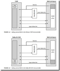
The Infineon C509 microcontrollers have 3 kbytes of internal XRAM. By default, XRAM is disabled when the device is reset and the full 64 kbytes of external data memory are accessible.

However, if XRAM is enabled, then the internal XRAM and external RAM memory areas overlap: specifically, in the case of the C509, the XRAM is mapped to the upper 3 kbytes of data memory, as illustrated in Figure 6.4.

The internal XRAM is enabled via the SYSCON1 SFR. Specifically, the PRGEN bit must be set to 0 and the SWAP bit must be set to 1.

Example: Using external RAM and internal SRAM on the Dallas 8XC520

The Dallas 8XC520 microcontrollers have 1 kbyte of internal ‘SRAM’. By default, this SRAM is disabled when the device is reset and the full 64 kbytes of external data memory are accessible. However, if SRAM is enabled, then the internal XRAM and external RAM memory areas overlap: specifically, in the case of the 8XC520, the SRAM is mapped to the lowest 1 kbyte of data memory, as illustrated in Figure 6.5.

Memory issues-0112


Reset hardware:RC RESET

RC RESET
Context

● You are developing an embedded application using one or more members of the 8051 family of microcontrollers.

● You are designing an appropriate hardware foundation for your application.

Problem

How do you create a low-cost reset circuit for your 8051 microcontroller?

Background

As discussed in the introduction to this chapter, the reset process which must be com- pleted prior to the execution of any other code requires that the microcontroller’s oscillator is operating. To trigger the reset operation, the original members of the 8051 family have a ‘RESET’ pin. When this is held at Logic 0, the chip will run nor- mally. If, while the oscillator is running, this pin is held at Logic 1 for two (or more) machine cycles, the microcontroller will be reset.

Note that, if the reset operation is not completed correctly, the microcontroller will usu- ally not operate at all: in rare circumstances, it may operate, but incorrectly. In either event, there is usually nothing that you can do, in software, to recover control of the system. Clearly, therefore, ensuring correct reset operation is a crucial part of any application.

Solution

Various techniques may be used to ensure that – when power is applied to your 8051- based application – the reset process is automatically carried out. The most widely used techniques are based on the use of an external capacitor and resistor: these tech- niques are considered in detail here.

RC reset circuits

A typical RC reset circuit is as shown in Figure 5.1.

The circuit in Figure 5.1 operates as follows. We assume that Vcc is initially at 0V (that is, the power has not been applied to the system) and that the capacitor C is fully discharged. When power is applied, the capacitor will begin to charge. Initially, the voltage across the capacitor will be 0V and – therefore – the voltage across the resistor (and the voltage at the RESET pin) will be Vcc: this is a Logic 1 value. Gradually, the capacitor will charge and its voltage will rise, eventually to Vcc: at this time, the voltage at the reset pin will be 0V.

Reset hardware-0091

In the real system, the microcontroller’s input voltage threshold is around 1.1 – 1.3V10: input voltages below this level are interpreted as Logic 0 and voltages above this level are interpreted as Logic 1. Thus, the reset operation will continue until the voltage at the RESET pin falls to a level of around 1.2V.

We can use this information to calculate the required values of R and C. To make this calculation, we use the fact that the capacitor in Figure 5.1 will have a voltage (Vcap) at time (t) seconds after it begins charging, given by Equation 5.1.

Reset hardware-0092

Note that Equation 5.1 assumes that the capacitor begins charging at a voltage of 0 and that the power supply voltage increases from 0V to Vcc in an instantaneous ‘step’ (rather than a slow ramp): these assumptions, although often made, are frequently invalid: see ‘Safety and reliability issues’ for a discussion of these issues.

The Intel 8051 data sheet recommends values of 8.2K for R and 10uf for C when this form of reset circuit is used. Figure 5.2 substitutes these values into Equation 5.1 and plots the result over a period of 500 ms.

When looking at Figure 5.2, remember that all 8051s complete their reset oper- ation in 24 oscillator periods or less: if we use a 12 MHz oscillator, this is a maximum period of 0.002 ms: by contrast, the recommended reset circuit takes around 100 ms to complete the reset operation. This may seem like an excessive reset period

1. The data sheet for your chosen microcontroller will provide a precise value, if you require it.

Reset hardware-0093

but, for reasons discussed under ‘Safety and reliability issues’, allowing approximately 100 ms for the reset is generally good practice.

Choosing values of R and C

If, having reviewed all aspects of this pattern, you have decided to use an RC-based reset circuit, what values of R and C should you use?

Rather than trying to determine values of R and C directly from Equation 5.1, we can simplify matters by noting that the product of R (in Ohms) multiplied by C (in Farads) is known as the ‘time constant’ (in seconds) of this form of RC circuit. This time con- stant is the time taken for the capacitor to be charged to 60% of its final voltage. Thus, with a 5V supply and the circuit in Figure 5.1, this is the time taken for the capacitor voltage to reach 3V and, therefore, the voltage at the reset pin to reach 2V (that is, Vcc – 3V): this is still high enough (because it is greater than 1.2V, as already discussed) to ensure that the device is in reset mode. As long as the device is still in this mode until approximately 1 ms after the power supply reaches Vcc (typically around 100 ms after starting: see ‘Safety and reliability issues’), the device will be reset correctly.

A basic rule of thumb, therefore, is that the RC time constant should be approxi- mately 100 ms and values of R and C chosen to meet this requirement will usually ensure effective reset operation (Equation 5.2):

Reset hardware-0094Reset hardware-0095

We can summarize the key material in this section as follows:

● A combination of a 10K resistor and a 10 µF capacitor in a RC reset circuit gives a 100 ms time constant. Bearing in mind the general limitations of RC reset circuits (see ‘Safety and reliability issues’), this value is suitable for the majority of 8051- based systems.

● The standard 8K2, 10 µF RC reset combination gives a time constant of 82 ms: this is generally adequate.

● Values of 1K and 10 µF (which appear in some books) provide a time constant of only 10 ms: these values will not provide a reliable reset operation with all power supplies.

Adding a RESET button

In some systems, it is helpful to have a reset button, to force a hardware reset. This is easy to achieve. Figure 5.4 shows a suitable circuit.

Reset hardware-0096

Note that the reset button pulls the RESET pin (assumed to be active high: see ‘Portability’) to Vcc. Note also that this button also discharges the capacitor, ensuring that – when the switch is released – the proper reset process will be carried out.

Hardware resource implications

This pattern has no implications for CPU or memory usage.

Reliability and safety issues

There are a number of reliability and safety issues related to the use of RC reset circuits. The key issues are considered in this section.

Overall, however, we make the recommendation as seen in the box.

Many of the reliability problems with embedded systems can be traced back to defects in the reset circuit. If cost is the only concern, consider using an RC reset: if reliability is a consideration, use a ROBUST RESET [page 77].

Time taken for power supply to reach steady state

Suppose you are developing an embedded industrial control system and you want to ensure that the system begins operating as soon as possible after power is applied. You note (from ‘Solution’) that the reset process on an 8051 microcontroller (with a 12 MHz oscillator) will take 0.002 ms. You conclude that, allowing a reset period of 1 ms (rather than the 100 ms figure recommended earlier) will provide sufficient margin for error.

Suppose you adjust the values to reduce the reset period to around 1 ms. For exam- ple, Figure 5.5 shows the result of using a 0.1 µF capacitor and a 6K7 resistor.

This combination of values may, sometimes, work: but in most systems it will fail. The reason is that real power supplies do not switch instantly from 0V to their specified output voltage: in reality, many supplies take 50 ms or 100 ms to reach this voltage when first switched on. You need to allow for this ‘ramped’ voltage input in your design.

If the supply voltage increases slowly, then the capacitor in your RC reset circuit will comparatively quickly charge up and will simply ‘follow’ the increasing power supply voltage. As a result, Vreset will be held at Logic 0 many milliseconds before the chip reaches its operating voltage (~5V). Therefore, the chip will only be ready to run its reset routine after the RESET signal is complete and no reset will be performed. Your application will therefore not start correctly.

If you really must have a rapid reset and you have control over the design of the power supply there are various ways of dealing with this problem. You may, for example, be able to increase the transformer capacity or reduce the values of these filter capacitors. Note, however, that tying the operation of a device to a particular power

Reset hardware-0097

supply will make your system design much less portable. If, to give a common example, your company subsequently decides to ‘outsource’ the power supplies or to use a single power supply across a range of different boards, you can quickly run into difficulties.

Time taken for oscillator to start

If the start of the (crystal) oscillator in your circuit is delayed the RC reset cycle may be completed before the oscillation begins. If this happens, the chip will not be reset.

Typical start-up times for crystal oscillators are 0.1 to 10 ms: however, the time taken for a crystal oscillator to start operating depends on its being mounted correctly and having appropriate capacitors. These issues are discussed in detail in the pattern CR YST AL OSCILLA TOR [page 54].

Handling brownouts and other power disruptions

Potential problems with reset circuits do not, unfortunately, only arise when embed- ded devices are first powered up. Consider, for example, Figure 5.6. This shows changes in the system supply voltage (nominally 5V) in the presence of two prob- lems. The first of these (at time = 4 seconds) is a simple power ‘glitch’, where the supply voltage drops briefly to 0V. The second problem (beginning at time = 14 sec- onds) is a ‘brownout’ condition: this means that the (mains) supply voltage is reduced significantly for a period of time, but the supply does not fail completely. These types of fault are comparatively common in mains-powered systems.

To ensure our system operates in a predictable manner, we need to be able to deal with each supply problem. In most systems, the power glitch will not pose a signifi- cant hazard. When the power fails, the voltage drops rapidly (to 0V) and the system will stop operating. When the power returns, the system will be reset in the usual way.

Reset hardware-0098

The brownout is potentially more problematic. If the supply voltage drops below the minimum operating voltage (typically 4.5V for most members of the family, although this varies), the microcontroller will stop operating. If the voltage then rises again, the microcontroller will begin to operate again; however, if using a simple RC reset, the device will not be reset. The results are difficult to predict and the RC reset circuit is therefore neither reliable nor safe if brownouts are a possibility: see ‘Related patterns and alternative solutions’ for some alternative techniques.

Portability

Some portability issues, related to the different performance of various power supplies, have been considered elsewhere in this pattern. These will not be discussed further here.

Note also that, as discussed in a following example, not all 8051 family members have ‘active high’ resets: some are ‘active low’. While the underlying principles are the same, the wiring of ‘active high’ and ‘active low’ resets are fundamentally incom- patible (see ‘Example: Working with active low resets’).

Overall strengths and weaknesses

RC reset circuits are cheap to implement.

RC resets are well understood and widely used in other microprocessor and microcontroller systems.

If your system is mains powered and safety and reliability are not issues (and cost is) this technique may be a good solution.

If the system power supply characteristics are unknown or vary or are subject to brownout, the reset operation may not always be effective: RC resets are generally not suitable for main-powered applications which must be reliable or safe.

Related patterns and alternative solutions

The pattern ROBUST RESET [page 77] describes a more expensive but generally much more reliable reset solution.

Example: Minimal Atmel 89C2051 circuit with crystal and RC reset

A minimal Atmel 89C2051 circuit, using an RC reset, is shown in Figure 5.7. Please see the pattern CR YST AL OSCILLA TOR [page 54] for details of the oscillator circuit.

Note that the Atmel device does not support external memory so that the /EA pin is not present: see the ‘memory patterns’ (Chapter 6) for details.

Reset hardware-0099

Example: Working with active low resets

The reset circuits considered so far have been ‘active high’ in nature. This means that normally the RESET pin will be held at a low level (~0V): to effect a reset, the RESET pin needs to be pulled high (~Vcc), while the oscillator is running.

However, some 8051 devices have ‘active low’ inputs: these can be identified by the presence of a RESET pin. As the name suggests, these pins are held at a high level during normal operation and must be pulled low (again usually for 24 clock cycles) to effect a reset. Examples of 8051 devices with active low inputs include the Infineon C509, C515C and C517A. All of these are popular and widely used devices.

Reset hardware-0100

Wiring an active low reset circuit is straightforward. Figure 5.8 shows a possible cir- cuit for these various active low devices.


Reset hardware:ROBUST RESET

ROBUST RESET

Context

● You are developing an embedded application using one or more members of the 8051 family of microcontrollers.

● You are designing an appropriate hardware foundation for your application.

Problem

How do you create a very reliable reset circuit for your 8051 microcontroller?

Background

See RC RESET [page 68] for some background material on reset circuits.

Solution

As discussed in RC RESET [page 68], a key problem for the designers of reliable embed- ded systems is that power supplies are seldom ideal. For example, mains power supplies can take around 100 ms to reach their normal operating voltage when first switched on and may subsequently suffer from voltage variations, including brownouts, in part due to variations in the network load caused by other users of the mains supply. On the other hand, ‘1.5V’ primary cells (‘batteries’) often begin life with a voltage of up to 1.7V and decline to 0.9V or less as they are used.

Although careful design of your power supply can reduce these problems, it is often desirable to reduce the risks of system failure by maximizing the chances that your system will be reset correctly in the event of power supply problems. The robust reset circuits, notably from Dallas and Maxim, directly address this problem.

These useful devices perform two basic operations:

● When power is applied to a ‘cold’ system, they apply an appropriate (active high or active low) reset signal to the microcontroller for at least 100 ms to allow the oscil- lator (if used) and power supply to reach their operational state.

● If the supply voltage falls below a preset value during normal operation, the reset cycle will begin and will only end ~100 ms after the supply is restored to the normal value. This behaviour deals with both total power failures (long or short) and brownouts.

Overall, these devices are very effective and are cheap. Except where cost is the only concern, they are highly recommended.

Hardware resource implications

This pattern has no implications for CPU or memory usage.

Reliability and safety issues This form of reset circuit is, as a general rule, much safer than any RC-based equivalent.
Portability

The various robust reset chips are generally insensitive to power supply variations over a wide range: use of such devices therefore tends to make your design more portable and less dependent on a particular power supply. Most devices are available with both ‘active high’ and ‘active low’ versions and are therefore compatible with a wide range of 8051 chips.

Overall strengths and weaknesses

Robust reset provides reliable performance even with ‘slow’ power supplies and in the event of brownout.

More expensive than RC reset alternatives.

Related patterns and alternative solutions

RC RESET [page 68] offers a cheaper alternative where safety and reliability are much less important than product cost.

In addition, two further ways of obtaining reliable reset behaviour are now discussed.

On-chip reset circuits

Reset circuits are always a challenge with microcontroller-based systems and – now that small reset ICs are available – it seems surprising that this circuitry is not simply included in the microcontroller itself.

In fact, in more recent 8051s, such circuitry is included: see, for example, the Dallas DS87C520 / DS83C520 and the Philips 87LPC764. An example of a Dallas 87C520 circuit using internal reset components is given in the following section.

Microcontroller / microprocessor supervisor ICs

The robust reset circuits discussed here are simple, economical reset options. However, in some applications, we require other external facilities too. Maxim, in particular, have developed a range of different ‘microcontroller supervisor’ ICs that include not only the equivalent of ‘robust reset’ circuits, but also have various combinations of additional facilities, such as watchdog timers and even RS-232 transceivers. Three examples of such devices are summarized here: consult the Maxim WWW site11 for further details.

11. www.maxim-ic.com

Max6330/1: Reset control, plus 3V / 3.3V / 5V shunt regulator. This allows a single, inexpensive IC chip to be used for both the power supply regulation and reset circuit.

Max819: Reset control plus watchdog, plus battery switchover.

Max3320: Reset control, plus RS-232 transceiver.

In addition, the ‘1232’ power monitor (available in various versions from both Dallas and Maxim) combines ROBUST RESET behaviour with a watchdog timer: as we see in Chapter 12, this is a very useful combination in many applications.

Example: Using the Dallas DS1812 ‘Econoreset’ with the 8051 family

Please refer to Chapter 26, Figure 26.10, for one of many examples in this book that use the DS1812 robust reset with the Standard 8051 device.

Example: Using Dallas ‘Econoresets’ with the Infineon C515C-8E

A minimal Infineon C515C-8E circuit, created using a Dallas DS1811 robust reset, is shown in Figure 5.9.

Reset hardware-0101

Example: Using the Max810M with the Infineon C501-1E

A minimal Infineon C501-1E circuit, created using a Maxim 810M robust reset, is shown in Figure 5.10.

Example: Minimal Dallas circuit using on-chip reset circuit

As noted earlier, some more recent 8051 devices have on-chip reset circuitry.

Reset hardware-0102

As an example, we will consider the DS87C520 (see Figure 5.11), whose circuitry operates as follows. While powering up, the internal monitor circuit maintains a reset state until Vcc rises above the ‘reset’ level. Once above this level, the monitor enables the oscillator input and counts 65,536 clock cycles, before leaving the reset state. This power-on reset (POR) interval allows time for the both the power supply and oscilla- tor to stabilize. In addition, if the supply voltage drops during normal operation, power monitor will generate and hold a reset automatically.

Note that this solution works with many of the Dallas ‘high speed’ and ‘ultra high speed’ devices, including the 80C320, 80C323, 83C520, 87C520, 87C530, 87C550 and 89C420.

Reset hardware-0103