Computer Systems:PC Hardware

PC Hardware

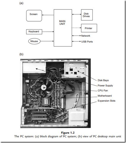
Inside the PC main unit (Figure 1.2b), the traditional motherboard has slots for expansion boards and memory modules to be added to the system. The power supply and disk drives are fitted separately into the main unit frame. The keyboard and mouse interface are integrated on the motherboard. In older designs, expansion boards carried interface circuits for the disk drives and external peripherals such as the display and printer, but these functions are now increasingly incorporated into the motherboard itself. Peripherals are now usually connected via USB or wirelessly.

The desktop PC is a modular system, which allows the hardware to be put together to meet the individual user’s requirements, with components sourced from different specialist suppliers, and allows subsystems, such as disk drives and keyboard, to be easily replaced if faulty. This also allows easy upgrading (e.g. fitting extra memory chips) and also makes the PC architecture well suited to industrial applications. In this case, the PC can be ‘ruggedized’ (put into a more robust casing) for use on the factory floor. This modular architecture is one of the reasons for the success of the desktop PC hardware, which has continued in the same basic form for many years, as a universal processor platform. The laptop is the main alternative for the general user, but it is not so flexible, and tends to be replaced rather than upgraded. Another reason for its success is the dominance of Microsoft operating systems, which have developed in conjunction with the Intel-based hardware, providing a standard platform for domestic, commercial and industrial computers.


Computer Systems:Personal Computer System

Personal Computer System

The conventional desktop system comprises a main unit, separate keyboard and mouse, and monitor. The main unit has connectors for these (when wireless peripherals are not available) and universal serial bus (USB) ports for memory sticks, printers, scanners, etc., as well as hardwired (Ethernet), or wireless (Wi-Fi) network interfaces. The circuit board (motherboard) in the main unit carries a group of chips which work together to provide digital processing of information and control of input and output devices. A power supply for the motherboard and the peripheral devices is included in the main unit.

The laptop has the same components in a compact form, with integrated keyboard and screen, while tablet computers are even more compact with a touch-sensitive screen and no keyboard. The difference between a microprocessor and microcontroller system is illustrated quite well by comparing a desktop computer with a touch-screen game console or mobile phone. The facilities and applications are similar, they just differ in scale and complexity.

A block diagram (Figure 1.2a) is a good way to show such a system in simplified form, so we can identify the main components and how they connect. In the case of the disk drives and network, for example, the information flow is bidirectional, representing the process of saving data to, and retrieving data from, the hard disk or server. The internal architecture of a microcontroller is shown in its data sheet as a block diagram.

Any microprocessor or microcontroller system must have software to run on the hardware. In a desktop, this is stored on a hard disk inside the main unit; this can hold a large amount of data that is retained when the power is off. There are two main types of software required: the operating system (e.g. Microsoft® Windows) and the application (e.g. Microsoft® Word). As well as the operating system and application software, the hard disk stores the data created by the user, in this case, document files.

The keyboard is used for data input, and the screen displays the resulting document. The mouse provides an additional input device, allowing control operations to be selected from menus or by clicking on icons and buttons. This provides a much more user-friendly interface than earlier computers, which had a command-line interface. Then, actions were initiated by typing a text command such as ‘dir’ to show a directory (folder) of files. Network specialists still use this type of interface as it allows batch files (list of commands) to be created to control system operation. The network interface allows us to download data or applications from a local or remote server, or share resources such as printers over

a local area network (LAN) and provide access to a wide area network (WAN), usually the Internet. In the domestic environment, a modem is currently needed to connect to the Internet via a telephone line or cable service. The network browser (e.g. Microsoft® Internet

PIC Microcontrollers-1114


Using ‘SPI’ peripherals

Introduction

When using asynchronous serial protocols, such as ‘RS-232’, the two devices that are communicating must agree on a communication frequency (the baud rate) and each device then uses (say) an independent crystal-based clock to ensure that it operates at the required rate. One consequence of this approach is that, if the clocks in the transmitter and receiver devices vary by more than a few per cent, the receiving device will be unable to decode the incoming data correctly.

By contrast, the serial peripheral interface (SPI) uses a synchronous communication protocol: this means that both the transmitter and receiver devices share a common clock. The transitions of this common clock determine when to send and receive the various bits. For example, in a simple synchronous protocol, the transmitter device may write a bit on the rising edge of the clock and the receiving device will then read this bit when it detects the falling clock edge. Note that the clock frequency does not need to be held constant.

Such synchronous interfaces are primarily intended for use over distances meas- ured in centimetres rather than in metres and we will restrict our discussions here to the use of SPI to link the 8051 with compatible peripherals.


Example: I2C EEPROM interface

Example: I2C EEPROM interface

In this example we consider how to link an 8051 microcontroller to a serial EEPROM using an I2C bus. Note that use of such EEPROMs is a common way of retaining system settings after power is removed: the storage is non-volatile, for a period of around 100 years.

Hardware

The required hardware is illustrated in Figure 23.6.

Note that, in this case, we are not using an open-collector port and do not require pull-up resistors. If you are using more than one I2C device, it is recommended that you adapt the code to work with Port 0 (a trivial change) and use pull-up resistor values calculated as described in ‘Background’.

Software

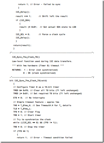
The required software is contained in Listings 23.4 to 23.6. Note that you will also require the core I2C library from the ‘Solution’ section.

image

image

image

image

image

image


Example: I2C core library

Example: I2C core library

In this section we present a library of core I2C routines (Listings 23.1 to 23.3). In most cases you will need to add some additional functions to use these files with particular I2C peripherals: we illustrate this process in the examples that follow.

Please note that not all I2C devices use ACKNOWLEDGE / NOT ACKNOWLEDGE

signals (discussed earlier). Similarly, not all devices need a ‘read byte’ facility (PWM and DAC outputs, for example). You can omit these library features by means of these lines at the top of the I2C_Core.C file:

image

image

image

image

image

image

image

image


Example: I2C Temperature sensor interface

Example: I2C Temperature sensor interface

In this example we consider how to link an 8051 microcontroller to Dallas DS1621 (I2C) temperature sensor.

Hardware

See Figure 23.4.

Software

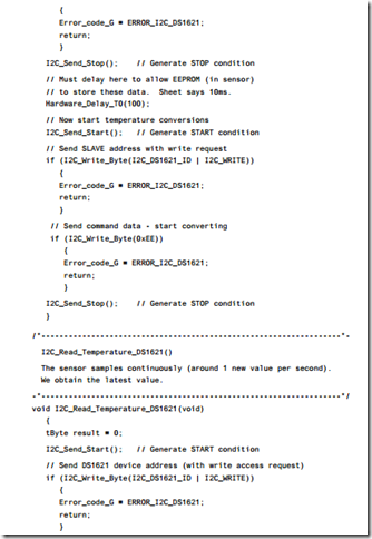
The key software files are in Listings 23.7 to 23.9: all the files required for the project are included on the CD, in the directory associated with this chapter.

image

image

image

image

image


Using peripherals:I2c peripheral

I2c peripheral

Context

● You are developing an embedded application using one or more members of the 8051 family of microcontrollers.

● The application has a time-triggered architecture, based on a scheduler.

● The microcontroller in your application will be interfaced to one or more peripherals, such as a keypad, EEPROM, digital-to-analog converter, or similar device.

Problem

Should you use the I2C protocol to link your microcontroller to peripheral devices and, if so, how do you do so?

Background

There are five key features of I2C as far as the developer of embedded applications is concerned:

● I2C is a protocol designed to allow microcontrollers to be linked to a wide range of different peripherals – memory, displays, ADCs and similar devices – and requires only two port pins to connect to (typically) up to 20 peripherals.

● There are many I2C peripherals available for purchase ‘off the shelf’.

● I2C is a simple protocol and may be easily generated in software. This allows all 8051 devices to communicate with a wide range of peripheral devices.

● A common set of software code may be used with all I2C peripherals.

● I2C is fast enough (even when generated in software) to be compatible with time- triggered architectures. Typical data transfer rates will be up to 1,000 bytes / second (with a 1 ms scheduler tick).

We provide some background necessary for understanding and using the I2C bus in this section. Please note that much of the material here is adapted from the Philips (1998) I2C specification. For further details, the reader is referred to this document, a copy of which can be obtained from the Philips WWW site.1

Hardware

We begin by considering essential I2C hardware features.

The bus

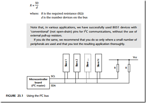
In the two-wire I2C bus the serial data (SDA) and serial clock (SCL) lines carry the information between the various devices (Figure 23.1). Due to the variety of different technologies (CMOS, NMOS, bipolar) used to create devices which can be connected to the I2C bus, the levels of the logical ‘0’ (LOW) and ‘1’ (HIGH) are not fixed and depend on the system supply voltage.

When the bus is free, both SCL and SDA lines are HIGH.

Both SDA and SCL are bidirectional lines. The output stages of devices connected to the bus should be open drain (open collector) in order to match the requirements of this protocol. This will often mean using pins on Port 0 of an 8051 device (but see following box).

The number of devices that can be connected to the I2C bus is limited only by the maximum bus load capacitance of 400 pF: in the absence of suitable information, assume that each peripheral device and its wiring contributes a total of 20 pF to the total capacitance.

Each of the lines is connected to the Vcc supply via a common pull-up resistor. If we assume a capacitance of 20 pF per device, the required value of resistor is deter- mined by the maximum rise time in the I2C specification (1,000 ns in Standard I2C). This can be shown to translate into the following:

image

Device addresses

In I2C, the communication is address based: that is, each device on the bus has a unique address and messages can be directed from anywhere on the bus to the device with a particular address.

The device addresses are ten-bits long in the latest version of this standard (seven bits in the original), allowing more than 1,000 different addresses to be used. Note that devices with 7-bit and 10-bit addresses may be used on the same bus.

While the facility for 7-bit or 10-bit addresses are included in the I2C specification,

in most practical cases, the address of a device is partially hard wired into the device.

Consider, for example, a useful I2C peripheral, the Atmel 24C64 serial EEPROM.2 This device provides 8192 × 8 bits of non-volatile data storage, with data retention for 100 years. As such it is ideal, for example, for storing small amounts of data in moni- toring applications or for storing system passwords in other devices.

The pinout of the 24C64 is given in Figure 23.2. Note from the figure that there are only three address lines, which will usually be pulled to Vcc or ground to set the required device address. Assuming each device is given a unique address, up to eight 24C64s may be connected to one I2C bus, rather than 128 (27) or 1024 (210) as is sug- gested by the I2C standard.

image

As far as the bus is concerned, the 24C64 has, in fact, a 7-bit address. However, the most significant four bits are ‘hard wired’ into the device. These bits are always ‘1010’ (0xA0), which is a code common to many serial EEPROMs. The full device address is therefore ‘1 0 1 0 A2 A1 A0’.

The hard-wiring of part of the device address makes practical sense. Few applications require more than eight serial EEPROMs on a single bus, particularly since quite large capacity memory devices are now available with an identical interface. If the full device address needed to be coded by the user for each device, the size of each chip would have to be increased to allow for (at least) four more pins (Figure 23.3).

Very similar schemes are used in other I2C devices. For example, the Dallas 1621 temperature sensor3 is a useful and inexpensive component that provides a tempera- ture reading, in Celsius, over an I2C bus (Figure 23.4).

image

Here, again, only three least significant bits of the address are user adjustable. In this case, the full address of the device is ‘1 0 0 1 A2 A1 A0’. The hard-wired part of this address (0x90) is shared by many DAC devices.

The I2C protocol: Masters and Slaves

Each device on an I2C bus can operate as either a transmitter or receiver of data. For example, an LCD driver will generally act as a receiver, whereas a memory device can act as both a receiver and a transmitter. In addition to transmitters and receivers, devices can also be considered as Masters or Slaves. A Master is the device which initi- ates a data transfer on the bus and generates the clock signals to permit that transfer. At that time, any device addressed is considered to be a Slave.

The I2C bus has a multi-Master capability: this means that more than one device

capable of controlling the bus can be connected to it. This might be the useful, for example, if I2C were used to transfer data between two microcontrollers.

Please note that in this pattern we are concerned only with I2C applications involv- ing a single microcontroller (the device Master) and one or more Slave peripherals.

Generation of clock signals on the I2C bus is always the responsibility of a Master device; the Master generates its own clock signals when transferring data on the bus. In a single-Master system, bus clock signals from a Master can only be altered when they are stretched by a slow Slave device holding down the clock line.

Performing data transfers

We now consider how data are transferred between devices. Consider, for example, that we wish to read a temperature value from a DS1621 temperature sensor discussed earlier: we would do so as follows:

1 Generate a START condition

2 Send DS1621 device address (with WRITE access request)

3 Make sure that the Slave (DS1621) generates an ACKNOWLEDGE bit

4 Send the command ‘Read Temperature’ (0xAA)

5 Make sure that the Slave (DS1621) generates an ACKNOWLEDGE bit

6 Generate another START condition

7 Send DS1621 device address (with READ access request this time)

8 Make sure that the Slave (DS1621) generates an ACKNOWLEDGE bit.

9 Receive the first (most significant) byte of temperature data from the I2C bus

10 Perform a MASTER – ACKNOWLEDGE

11 Receive the second byte of temperature data from the I2C bus

12 Perform a MASTER – NOT ACKNOWLEDGE

13 Generate a STOP condition

Although this process appears at first glance rather complex, it contains all the core I2C routines that are required for communication with any I2C peripheral. As a result, when we have considered this process, you will be in a position to develop I2C inter- faces for a very wide range of devices.

To understand the discussions that follow, it will be helpful to refer to Figure 23.5. We begin by considering the START and STOP conditions.

image

START and STOP conditions

I2C communications begin with a START condition. Further START conditions may be generated within the message, which will end with a STOP condition.

A START condition is represented as follows (see Figure 23.5): a HIGH to LOW transition on the SDA line while SCL is HIGH.

A STOP condition is represented as follows (see Figure 23.5): a LOW to HIGH transition on the SDA line while SCL is HIGH.

START and STOP conditions are always generated by the Master.

Byte format

Every byte put on the SDA line must be eight bits long. The number of bytes that can be transmitted per transfer is unrestricted. Each byte has to be followed by an ACKNOWLEDGE bit (see following sections).

Data are transferred with the most significant bit first. If a Slave cannot receive or transmit another complete byte of data until it has performed some (internal) oper- ation, for example updating memory, it can hold the SCL line LOW to force the Master into a wait state. Data transfer then continues when the Slave is ready for another byte of data and releases SCL.

Slave ‘ACKNOWLEDGE’ and ‘NOT ACKNOWLEDGE’

In many situations the Master (the microcontroller in our case) will be sending data to the Slave (for example, an EEPROM). In these cases, the ‘Slave-receiver’ must gener- ate an ‘Slave-receiver ACKNOWLEDGE’ signal when it has received a byte of data.

The ACKNOWLEDGE-related clock pulse is always generated by the Master. The transmitter releases the SDA line (HIGH) during the ACKNOWLEDGE clock pulse. The Slave-receiver must pull down the SDA line during the ACKNOWLEDGE clock pulse so that it remains stable LOW during the HIGH period of this clock pulse.

Usually, an active Slave-receiver is obliged to generate an ACKNOWLEDGE after each byte has been received.

When a Slave does not acknowledge the Slave address (for example, it is unable to receive or transmit because it is performing some internal operation), the data line must be left HIGH by the Slave. The Master can then generate either a STOP condi- tion to abort the transfer or a repeated START condition to start a new transfer.

If a Slave-receiver does acknowledge the Slave address but, some time later in the transfer cannot receive any more data bytes, the Master must again abort the transfer. This is indicated by the Slave generating a ‘NOT ACKNOWLEDGE’ response on the first byte to follow: this means that the Slave leaves the data line HIGH during the ACKNOWLEDGE clock pulse generated by the Master. The Master will then generate a STOP (or a repeated START) condition and – probably after a delay – will attempt the transmission again.

Master-receiver ‘ACKNOWLEDGE’ and ‘NOT ACKNOWLEDGE’

In some situations the Master (the microcontroller in our case) will be receiving data from the Slave (for example, the temperature sensor). In some cases, the ‘Master- receiver’ must generate a ‘Master-receiver ACKNOWLEDGE’ signal when it has received a byte of data. However, at the end of the data transfer (when the Master- receiver has received the last byte of data it requires), it must signal the end of data to the Slave-transmitter by not generating an ACKNOWLEDGE on the last byte that was clocked out of the Slave. The Slave-transmitter must release the data line to allow the Master to generate a STOP or repeated START condition.

Synchronization

All Masters generate their own clock on the SCL line to transfer messages on the I2C bus. Data are only valid during the HIGH period of the clock. A defined clock is there- fore needed for the bit-by-bit arbitration procedure to take place.

Clock synchronization is performed using the wired AND connection of I2C inter-

faces to the SCL line. This means that a HIGH to LOW transition on the SCL line will cause the devices concerned to start counting off their LOW period and, once a device clock has gone LOW, it will hold the SCL line in that state until the clock HIGH state is reached. However, the LOW to HIGH transition of this clock may not change the state of the SCL line if another clock is still within its LOW period. The SCL line will therefore be held LOW by the device with the longest LOW period. Devices with shorter LOW periods enter a HIGH wait-state during this time.

When all devices concerned have counted off their LOW period, the clock line will be released and go HIGH. There will then be no difference between the device clocks and the state of the SCL line and all the devices will start counting their HIGH peri- ods. The first device to complete its HIGH period will again pull the SCL line LOW. In this way, a synchronized SCL clock is generated with its LOW period determined by the device with the longest clock LOW period and its HIGH period determined by the one with the shortest clock HIGH period.

Further details

A complete technical specification for the I2C bus will be found on the Philips WWW site.

Solution

Should you use I2C?

In order to determine whether use of an I2C bus is appropriate in your time-triggered application, we consider some key questions that should be asked when considering the use of any communications protocol or related technique.

Main application areas

The I2C bus was designed mainly to allow the interconnection of components within a single application. Although the bus may be used, for example, to connect proces- sors (usually microcontrollers) to one another or to other computer systems, its main application area is in the connection of standard peripheral devices, such as LCD panels or EEPROMs, or ‘smart’ components in consumer applications (e.g. TV tuners, PLL synthesizers, video processors) to microcontrollers.

Ease of development

I2C can be used to communicate with a large number and range of peripherals. By using the same protocol to talk to a range of devices, development efforts may be reduced.

Scalability

The maximum size of an I2C bus is limited by the maximum capacitance of 400 pF. To estimate the maximum network size, we can add up the input capacitance of all the devices we wish to connect to the bus.

For example, the SGS-Thomson ST24C16 16K I2C-compatible EEPROM has an input capacitance of around 8 pF, and we could attach some 50 of these devices together on the same bus. Note that this rough calculation ignores any effects of stray capacitance due to the cabling itself. If we assume a ‘standard’ capacitance per device of 20 pF (including stray capacitance), we can still hope to connect around 20 periph- erals to the microcontroller over a single bus.

Overall, the bus supports large enough collections of peripherals to meet the needs of its main application area.

Flexibility

I2C is flexible. Networks of one Master and multiple Slaves and networks with multiple Masters can both be implemented. Note: we consider only single-Master applications in this pattern.

Speed of execution and size of code

As we have mentioned, I2C can operate over a wide speed range: from 100 kbits/s in the ‘standard’ version (1992), to 400 kbits/s in the ‘fast’ version, and now 3.4 Mbit/s in the latest ‘high-speed’ version introduced in 1998.

However, in this pattern we are concerned with I2C interfaces created entirely in software. Such interfaces are only practical at the low end of the speed range.

Generation of the I2C protocol inevitably adds to the code size: see the core I2C library (in the following example) for details.

Cost

The cost of licence fees for use of the bus is included in the cost of the peripheral components which you purchase: in most circumstances, there are no additional fees to pay.

Note that this may not be the case if, for example, you are implementing a I2C

peripheral (to be sold for connection to an I2C bus). If in doubt, please contact Philips for further details.

Choice of implementations and vendors

The I2C library presented here may be used with any 8051 device.

Suitability for use in time-triggered applications

As we saw in Chapter 18, the RS-232 communication protocol is appropriate for use in time-triggered applications. This suitability arises because the task duration associated with transmission (and reception) of data on an RS-232 network is very short. Note that this transmission time is not directly linked to the baud rate of the network, largely because almost all of the 8051 family have on-chip hardware support for RS- 232, with the result that messages are transmitted and received ‘in the background’.

The situation with I2C is rather different. Specifically, in this pattern, we are con-

cerned with software-based I2C protocols; this undoubtedly adds to the software load. For example, if we consider the process of sending one byte of data to an I2C-based ROM chip (an example of this is presented in full later), then the total task duration is approximately 0.5 ms.

This task duration can be supported on a time-triggered application, even with 1 ms timer ticks, if the maximum data rate (1000 bytes / second) matches the needs of the application.

How do you use I2C in a time-triggered application?

The examples that follow include a complete I2C library which may be used with any member of the 8051 family.


Example: Keypad library with buffer and fn key support

Example: Keypad library with buffer and fn key support

We present here a complete keypad library for the 8051 family. The library has support for function keys (two) and has a buffer facility. The library is intended to work with key- pads as shown in Figure 20.3, but is easily adapted to different keypad layouts and sizes.

The demonstration program runs on an Infineon c515c microcontroller. However, none of the keypad code is 515 specific: using appropriate versions of the scheduler and the PC link libraries (included on the CD) it can be used with any 8051 family member.

Figure 20.4 shows a typical program output.

The key library files are given in Listings 20.2 to 20.5. Refer to the CD for the com- plete set of files for this example.

image

image

image

image

image

image

image

image

image


Using peripherals:Hardware resource implications,Reliability and safety implications.

Hardware resource implications

I2C requires the use of two port pins. This is considerably fewer than would be required to create a parallel interface to most peripheral devices.

There is, however, a significant CPU load: see ‘Solution’ for details.

Reliability and safety implications

The I2C protocol incorporates only minimal error-checking mechanisms: detection of data corruption (for example) during the transfer of information to or from a peripheral device must be carried out in software, if required. However, in most cases, damage to cabling will be quickly detected.

Portability

I2C is a simple protocol and may be easily generated in software. This allows the tech- niques presented here to be used with all 8051 devices.

Overall strengths and weaknesses

I2C is supported by a wide range of peripheral devices.

I2C requires only two port pins to connect to (typically) up to 20 peripherals.

I2C is a simple protocol and may be easily generated in software. This allows

all 8051 devices to communicate with a wide range of peripheral devices. A common set of software code may be used with all I2C peripherals.

Although I2C is fast enough (even when generated in software) to be compatible with time-triggered architectures, typical data transfer rates will be comparatively slow (up to 1000 bytes / second with a 1 ms scheduler tick).

Related patterns and alternative solutions

See SPI PERIPHERAL [page 521].

Remember also that, if possible, the best approach is to avoid peripherals altogether and use a microcontroller with on-chip facilities if possible. For example, rather than using a basic 8051 plus serial EEPROM, consider using the Atmel AT89LS8252, which has two kbytes of EEPROM on the chip.