Microcontroller Operation:Register Pair Operations

Register Pair Operations

Table 2.3 shows basic operations that can be applied to pairs of registers. The result is retained in one of them, the destination register. The data to be combined with the contents of the destination register is obtained from the source register, typically W or a literal (number supplied in the instruction). The source register contents generally remains unchanged after the operation.

The meaning of each type of instruction is explained below, with examples from the PIC instruction set. As noted above, there is an option to store the result in W, the working register, if that is the source. Note also that the PIC 16 instruction set does not provide moves directly between file registers; all data moves are via W.

Status bits are modified by specific register operations. The zero flag (Z) is invariably affected by arithmetic and logic instructions, and the carry flag (C) by arithmetic ones, including rotate. The effect on the source, destination and status registers of each instruction is specified in the instruction set, and this needs to be studied thoroughly before attempting to write assembler programs. The binary, hex and assembler code is given, together with the flag(s) affected, if any, in the following examples.

PIC Microcontrollers-1134

Move

The most commonly used instruction in any program simply moves data from one register to another. It is actually a copy operation, as the data in the source register remains unchanged until overwritten.

00 1000 0000 1100 080C MOVF 0C,W (Z)

This instruction moves the contents of register 0Ch (1210) into the working register. Note that bit 7, selecting the destination, is ‘0’ for W, which has to be specified in the instruction.

00 0000 1000 1100 008C MOVWF 0C

This instruction is the reverse move, from W to register 0Ch. Bit 7 is now ‘1’, and the zero flag is not affected, even if the data is zero.

An example of the move instruction is seen at line 46 in the keypad program, MOVWF PORTC, which outputs a binary code to operate the display.

Arithmetic

Add and subtract are the basic arithmetic operations, carried out on binary numbers. Some processors also provide multiply and divide in their instruction set, but these can be created if necessary by using shift, add and subtract operations.

00 0111 1000 1100 078C ADDWF 0C (C,Z)

This instruction adds the contents of W to register 0C. The carry flag will store a carry-out of the most significant bit (MSB), if the result is greater than the maximum value, FFh (25510), with the remainder left in the register. For example, if we add the decimal numbers 200 and 100, the result will be 300. The remainder will be 300 – 256 ¼ 44, with the carry flag representing 256 (result ¼ 1 0010 1100 in binary). If the sum is exactly 25610, the register result will be zero (Z flag set) and carry-out generated (C flag set).

The carry flag is also included when subtracting, so that numbers up to 51110 can be operated on. Rotate can be used to halve and double binary numbers, while increment and decrement are also available.

Logic

Logical operations act on the corresponding pairs of bits in a literal or source register, and destination. The result is normally retained in the destination, leaving the source unchanged. The result in each bit position is obtained as if the bits had been fed through the equivalent logical gate (see Appendix B).

11 1001 0000 0001 3901 ANDLW 01 (Z)

This instruction carries out an AND operation on the corresponding pairs of bits in the binary number in W and the binary number 00000001, leaving the result in W. In this example, the result is zero if the LSB in W is zero, so it forms a check on the state of that bit alone.

This type of operation can be used for bit testing if the processor does not provide a specific instruction, or masking to select a portion of the source data. The AND operation gives a result 1 if BOTH source bits are 1. The OR operation gives the result 1 if EITHER bit is 1. XOR gives result 1 if ONE of the bits is 1. This covers all the options for logical processing.

An example of a logic instruction is seen at line 45 in the keypad program, ANDLW 0F0, which masks one of the digits for output to the display.


Microcontroller Operation:Single Register Operations

Single Register Operations

The processor operates on 8-bit data stored in RAM registers and W. The data can originate in three ways:

• A literal (numerical value) provided in the program

• An input via a port data register

• The result of a previous operation.

This data is processed using the set of instructions defined for that processor. Table 2.2

shows a typical set of operations that can be applied to a single register. The same binary number is shown before processing, and then after the operation has been applied to the register.

As an example of how these operations are specified in mnemonic form in the program, the hex and assembler code to increment a PIC register is:

0A86 INCF 06

Register number 06 happens to be port B data register, so the effect of this instruction can be seen immediately at I/O pins of the chip. The corresponding machine code instruction is 0A86h, or 00 1010 1000 0110 in binary (14 bits). As you can see, it is easier to recognize the mnemonic form. Bit 7 of the instruction code is significant in that it determines the destination of the result. The default is ‘1’, which causes the result to be left in the RAM register. ‘0’ places it in W, which helps to reduce the number of move instructions required.

An example of a single register operation appears at line 33 in the keypad program, CLRF PORTC, which sets all the output bits connected to the display to zero, switching it off.

PIC Microcontrollers-1133


Microcontroller Operation:Program Operations

Program Operations

We can see in Appendix A that a machine code program consists of a list of binary codes stored in the microcontroller memory. They are decoded in sequence by the processor block, which generates control signals that set up the microcontroller to carry out the instruction. Typical operations are:

• Load a register with a given number.

• Copy data from one register to another.

• Carry out an arithmetic or logic operation on a data word.

• Carry out an arithmetic or logic operation on a pair of data words.

• Jump to an alternative point in the program.

• Test a bit or word and jump, or not, depending on the result of the test.

• Jump to a subroutine, and return later to the same point.

• Carry out a special control operation.

The machine code program must be made up only from those binary codes that the instruction decoder will recognize. These codes can be read off from the instruction set given in the data sheet. When computers were first developed, this was exactly how the program was entered, in binary, using a set of switches. This is obviously time consuming and inefficient, and it was soon realized that it would be useful to have a software tool that would generate the machine code automatically from a program written in a more user-friendly form. Assembly language programming was therefore developed, when computer hardware had moved on enough to make it practicable.

Assembly language allows the program to be written using mnemonic (memorable) codes.

Each processor has its own set of instruction codes and corresponding mnemonics. For example, a commonly used instruction mnemonic in PIC programs is ‘MOVWF’, which means move (actually copy) the contents of the working register (W) to a file register that is specified as the operand. The destination register is specified by number (file register address), such as 0Ch (the first general purpose register in the PIC 16F84A). The complete instruction is:

MOVWF 0C

This is converted by the assembler software (MPASM.EXE) to the hexadecimal code specified in the instruction set:

008C

The binary code stored in program memory is therefore

0000001 0001100

Note that the instruction is 14 bits in total, with the operand represented, in this case, by the last seven bits, and the operation code the first seven. The op-code bits are used by the

instruction decoder to select the correct source and destination registers (W and SFR 0C) prior to the operation. A following clock edge will then trigger the copy operation on the internal data bus.

There are two main types of instruction, with four identifiable subgroups within each:

PIC Microcontrollers-1132

Together, these types of operations allow inputs to be read and processed, and the results stored or output, or used to determine the subsequent program sequence.

A complete assembly language example is shown in the final section of Chapter 1. Program 1.1 is the list file KEY690.LST, whose function is to read a keypad and display the inputs. The source code mnemonics are on the right, with the machine code in column 2 and the memory location where each instruction is stored in column 1.


Microcontroller Operation:Special Function Registers

Special Function Registers

These numbered registers provide dedicated program control registers and processor status bits. In the PIC, the program counter, port registers and spare registers are all mapped as part of a block that starts at zero and ends at 0Bh in the 16F84A. For example, the program counter is register number 02. The working register is the only one that is not located in the main register block, and is accessed by specifying it in the instruction.

All processors contain control and status registers whose bits are used individually to set up the processor operating mode, or record significant results from those operations. In the PIC 16, the status register is located at SFR 03. The most frequently used bit is the zero flag. This is internally set to 1 if the result of any operation is zero in the destination register (the register that receives the result). The carry (C) flag is another bit in the status register; it is set if the result of an arithmetic operation produces a carry-out of the most significant bit of the destination register, that is, the register overflows.

The status register bits are often used to control program sequence by conditional branching. Alternate sections of code are executed depending on the condition of the status flag. In the PIC instruction set, this is achieved by an instruction that tests the bit and skips the next instruction if it is 0 or 1. The bit test and skip instruction is generally followed by a jump instruction to take the execution point to another part of the program, or not, as the case may be. This will be explained more fully in the next section.

The most important SFRs in the 16F84A are listed in Table 2.1. The RAM is divided into blocks, where bank 0 contains registers 00h to 7Fh, bank 1 registers 80h to FFh and so on, that is, 128 registers per bank. The SFRs are located at the bottom (lowest addresses) of each register bank (but the data sheet RAM block diagram shows them at the top). Some registers are duplicated in different banks (e.g. program counter, PCL), while others are unique data direction register, TRISA). More complex chips that need more registers have extra banks of RAM. For example, the 16LF1826 has eight. The exact arrangement for each chip

PIC Microcontrollers-1131


Microcontroller Operation:Arithmetic and Logic Unit and Port Registers

Arithmetic and Logic Unit

This is a combinational logic block that takes one or two input binary words and combines them to produce an arithmetic or logical result. In the PIC, it can operate directly on the contents of a register, but if a pair of data bytes is being processed (e.g. added together), one must be in W. The ALU is set up according to the requirements of the instruction being executed by the timing and control block. Typical ALU/register operations are detailed later in this chapter.

Port Registers

Input and output in a microcontroller are achieved by simply reading or writing a port data register. If a binary code is presented to the input pins of the chip by an external device (e.g. a set of switches), the data is latched into the register allocated to that port when it is read in the program. This input data can then be moved (or more accurately, copied) into another register for processing. If a port register is initialized for output, the code moved to its data register is immediately available at the pins of the chip. It can then be displayed externally, for example, on a set of light-emitting diodes (LEDs).

Each port has a ‘data direction’ register associated with its data register. This allows each pin to be set individually as an input or output before the data is read from or written to the port data register. A ‘0’ in the data direction register sets the port bit as an output, and a ‘1’ sets it as an input. These port registers are mapped (addressed) as SFRs, starting from register 05 for port A, 06 for port B, and so on in the original PIC 16 specification. In more recently introduced chips (e.g. 16LF1826), which need more registers, the ports start at 0Ch (h is a suffix indicating a hexadecimal number; see Appendix A). The port data direction registers are mapped into a second register bank (bank 1) with addresses starting at 85h for port A, 86h for port B, and so on.


Microcontroller Operation:Instruction Register and Decoder

Instruction Register and Decoder

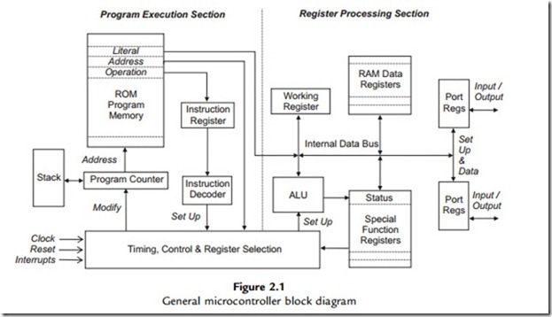
To execute an instruction, the processor copies the instruction code from the program memory into the instruction register (IR). It can then be decoded (interpreted) by the instruction decoder, which is a combinational logic block which sets up the processor control lines as required. These control lines are not shown explicitly in the block diagram, as they go to all parts of the chip, and would make it too complicated. In the PIC, the instruction code includes the operand (working data), which may be a literal value or register address. For example, if a literal (a number) given in the instruction is to be loaded into the working register (W), it is placed on an internal data bus and the W register latch enable lines are activated by the timing and control logic. The internal data bus can be seen in the manufacturer’s block diagram (Figure 1-1 in the PIC 16F84A data sheet).

Timing and Control

This sequential logic block provides overall control of the chip, sending signals to all parts of the chip to move the data around and carry out logical operations and calculations (see Appendix C). A clock signal is needed to drive the program sequence; it is traditionally derived from an external crystal oscillator, which provides an accurate, fixed frequency signal. More recent chips have an internal oscillator, which saves on external components.

A maximum frequency of operation is always specified; most current PIC 16 chips run at a maximum of 20 MHz, although newer designs reach 32 MHz. All can operate at any frequency below this maximum, down to 0 Hz. This is referred to as a static design: the clock can be stopped and the current MCU status will be retained. It takes four clock cycles to execute one instruction, unless it involves a jump, when it is eight. However, the execution of successive instructions overlaps to double the effective speed (pipelining; see data sheet).

The program starts automatically at program location zero, as long as the reset input is connected high (power-on reset). If required, a push button reset can be connected, which takes this input low for a manual reset. This should not normally be needed, but if there is a bug in the program or another system fault that causes the program to hang (get stuck in loop), a manual reset is useful, particularly during prototyping.

The only other way to stop or redirect a continuous loop is via an interrupt. Interrupts are signals generated externally or internally, which force a change in the sequence of operations. If an interrupt source goes active in the PIC 16, the program will restart at program address 004, where the sequence known as the ‘interrupt service routine’ (or a jump to it) must be stored. More details are provided in Chapter 6.


Microcontroller Operation:Program Memory and Program Counter

Program Memory

Microcontrollers used for prototyping and short production runs use flash memory to store the program. The program can be downloaded while the chip is in the application circuit (in-circuit programming). Alternatively, the chip is placed in a programming unit attached to the host computer for program downloading, before fitting it in the application board. For longer production runs, preprogrammed chips can be ordered from the manufacturer, which use mask programmed ROM, where the program is incorporated during chip fabrication.

The PIC 16 program consists of a list of 14-bit binary codes, each containing the instruction and operand (data) in one operation code. The program starts at address zero and the

instructions are executed in turn unless a branch instruction or an external ‘interrupt’ occurs. Usually, the last instruction causes a loop back to repeat the control sequence. The capacity of the program memory block is one of the most significant features of each PIC, varying from 1024 to 8096 instructions in the 16 series. The higher power PIC 18, 24, 32 and dsPIC ranges offer more memory, input/output (I/O) and peripheral features.

Program Counter

The Program Counter (PC) is a register that keeps track of the program sequence, by storing the address of the instruction currently being executed. It is automatically loaded with zero when the chip is powered up or reset. The program counter is file register number 2 in the SFR set. As each instruction is executed, PC is incremented (increased by one) to point to the next instruction. Program jumps are achieved by reloading PC to point to an instruction other than the next in sequence. This new address is provided in the instruction.

Often, it is necessary to jump from address zero to the start of the actual program at a higher address, because special control words must be stored in particular low addresses. Specifically, PIC 16 devices use address 004 to store the ‘interrupt vector’ (start address of the interrupt routine). In this case, the main program must not be located at address zero; instead, a jump to a higher address should be placed there. An assembler directive is then needed to place the start of the program at a higher address. This problem can be ignored for programs that do not use interrupts, and such simple programs will be located by default at address zero. Interrupts will be explained in more detail later.

Associated with the program counter is the ‘stack’. This is a temporary program counter store. When a subroutine is executed (see Chapter 5, Section 5.2.4), the stack register temporarily stores the current address, so that it can be recovered at a later point in the program. It is called a stack because the addresses are restored to the PC in the reverse order to which they were stored, that is, ‘last in, first out’ (LIFO), like a stack of plates.


Microcontroller Operation:Microcontroller Architecture

Microcontroller Architecture

The architecture (internal hardware arrangement) of a complex chip is best represented as a block diagram. This allows the overall operation to be described without having to analyze the internal circuit, which is extremely complex, in detail. PIC data sheets contain a definitive block diagram for each chip. Our starting point is the PIC 16F84A chip, because it has all the basic features but none of the more advanced elements that will be covered later. Also, the model for this chip is provided in the entry-level Proteus VSM microcontroller simulation package. Unfortunately, this chip is now effectively obsolete for new designs and is relatively expensive compared with more recently introduced chips, which actually have more features, such as the 16F690 that we will examine later on.

Simplified versions of the block diagrams from the data sheets will be used to help explain particular aspects of the chip operation. A general block diagram that shows some of the common features of PIC microcontrollers is seen in Figure 2.1. It shows that the MCU can be considered in two parts: the program execution section and the register processing section. Note that the program and data are accessed separately, and do not share the same data bus, as is the case within some processor systems. This arrangement, known as Harvard architecture, increases overall program execution speed. The timing and control block coordinates the operation of the two parts as determined by the program instructions, and responds to external control inputs, such as the reset and interrupts.

The program execution section contains the program memory, instruction register and control logic, which store, decode and execute the program. The register processing section has a block of random access memory (RAM), which starts with the special function registers (SFRs) that are used to control the processor operations, including the port registers, which are used for input and output. The rest of this RAM block provides general purpose registers (GPRs) for

PIC Microcontrollers-1130

data storage. The arithmetic and logic unit (ALU) processes the data, e.g. add, subtract and compare.

In some microcontrollers and microprocessors, the main data register is called the accumulator (A), but the name working register (W), used in the PIC system, is a better description. It holds the data that the processor is working on at the current time, and most data has to pass through it. For example, if a data byte is to be transferred from the port register to a RAM data register, it must be moved into W first. The working register works closely with the ALU in the data processing operations. Instructions may operate on W or on the RAM register, which includes the ports and SFRs.


Computer Systems:Programming a Microcontroller

Programming a Microcontroller

For the examples in this book, we will be using PIC chips that have flash ROM program memory, which can be easily erased and reprogrammed. This is very useful when learning, but also allows the firmware (microcontroller program) to be upgraded in any application, adding an app to a mobile phone, or upgrading its operating system. It is the same kind of memory used to store the image data in the SD card in the camera, and for general storage in a memory stick.

There are two ways of programming the PIC microcontroller. The preprogramming system is shown in Figure 1.10. The programming interface is the basic PICSTART Plus module, which accepts dual-in line (DIL) pin-out PIC chips up to 40 pins in a zero insertion force socket. The serial connection to the host PC COM port is made via an RS232 lead. This protocol is rather slow, and the COM port connector is not usually fitted to current PCs, so it is being replaced by USB in current programmers.

PIC Microcontrollers-1126

Alternatively, the PIC can be programmed in circuit, that is, after it has been fitted into the finished circuit board. This is known as in-circuit serial programming (ICSP), and the same hardware can also support in-circuit testing and debugging (ICD), as seen in Figure 1.11. The in-circuit programming module is the Microchip ICD2, which connects to the host via USB and to the target system via a six-way RJ-45 connector. In this case, the application board is the PIC Mechatronics demo board, which is used to investigate control of brushed dc motors and stepper motors.

The program is written as a text file and converted (assembled) to machine code (hex) in the host computer, using suitable development system software, usually Microchip MPLAB integrated development environment (IDE). Mistakes in the source code must be corrected before a hex file can be successfully created. The program operation can then be tested in MPLAB and downloaded to the target system.

Electronic computer-aided design (ECAD) software such as Proteus VSM also allows us to simulate the circuit on screen, in order to debug the program before downloading. The complete circuit can then be checked for correct operation, ideally by running the microcontroller in debug (fault-finding) mode, if this is supported by that particular device. All these techniques will be explained later on.

The basic technology for implementing digital systems is described in appendices at the back of this book. If you are not familiar with any of these hardware concepts, please refer to these sections as necessary. Appendix A covers information coding and assembler programs, Appendix B describes the basic electronics of digital systems, and Appendix C show how these work together to provide data input, storage, processing and storage devices.

PIC Microcontrollers-1127

PIC Microcontrollers-1128


Computer Systems:Microcontroller Application Design

Microcontroller Application Design

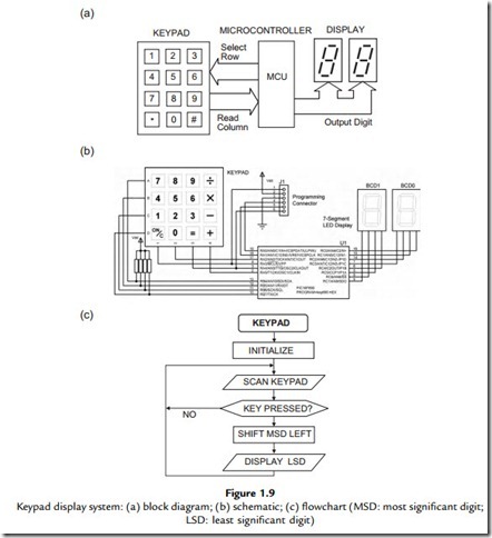
A simple microcontroller-based equivalent of the word-processing application described above is shown in Figure 1.9. The purpose of the system is to store and display numbers that are input on the keypad. Four inputs and three outputs are required for keypad connection to the microcontroller, but to simplify the drawing, these parallel connections are represented by the block arrows. The operation of the keypad is explained in more detail in Chapter 13 (see Figure 13.3). The seven segment displays show the input numbers as they are stored in the microcontroller. Each display digit consists of seven light-emitting diodes (LEDs), such that each digit from 0 to 9 is displayed as a suitable pattern of lit segments.

The basic display program works as follows: when a key is pressed, the digit is displayed on the right (least significant) digit, and subsequent keystrokes will cause the previously entered digit to shift to the left, to allow decimal numbers up to 99 to be stored and displayed. Calculations could then be performed on the data, and the result displayed. Obviously, real calculators have more digits, but the principle is the same.

The block diagram can then be converted into a circuit diagram using schematic capture software. Labcenter ISIS, part of the Proteus VSM package, has been used to create

PIC Microcontrollers-1120

Figure 1.9(b). A provisional choice of microcontroller must be made (which can be changed later) and the connections worked out. The PIC 16F690 has been selected here because it has a suitable number of inputs and outputs available, and is used on the Microchip Technology Inc. (Microchip) demonstration board to be studied later. A programming connector is also needed to get the program into the MCU. It is not necessary to include this in the block diagram, as it is implicit in the PIC design.

The starting point for writing the program for the microcontroller is to convert the general specification such as that given above into a description of the operations, which can be programmed into the chip using the set of instructions that are available for that microcontroller. The instruction set is defined by the manufacturer of the device. The process by which the required function is implemented is called the program algorithm, which can be described using a flowchart (Figure 1.9c).

PIC Microcontrollers-1121

This flowchart is now converted into a program, which is listed as Program 1.1. This source code is typed into a text editor and converted into a machine code program in the host PC, and downloaded to the chip via a programming module connected to the USB port (Figure 1.11). The main object of this book is to provide the reader with sufficient information to develop this kind of simple application, with a view to progressing to more complex projects. Proteus VSM allows the circuit to be tested on screen, with this program

PIC Microcontrollers-1122PIC Microcontrollers-1123PIC Microcontrollers-1124

attached to the MCU. Animated inputs and outputs provide instant results, allowing the program to be developed and debugged quickly and easily (see Appendix E). The list file shown contains the source code and machine code, which will be explained in the next chapter.

With suitable development of the software and hardware, the system could be modified to work as a calculator, message display, electronic lock or similar application; for example, more digits could be added to the display. Keyboard scanning and display driving are standard operations for microcontrollers, and the techniques mentioned here to create a working application will be discussed fully in later chapters.

PIC Microcontrollers-1125