PIC Architecture:Program Execution

Program Execution

The program consists of a sequence of 14-bit codes, which contain both the operation code and operand in a fixed length instruction. This machine code program is derived from a source code program created as a text file on a host PC, assembled and downloaded, as detailed in Chapter 4. At the moment we are not too concerned about exactly how the downloading is carried out; all we need to know for now is that the program is received in serial form from the host PC via an input/output (I/O) port pin (RB7/PGD/ICSPDAT). The data transfer is controlled by a data clock signal on an adjacent pin (RB6/PGC/ICSPCLK), while a high programming voltage (14 V) is applied to !MCLR. A low-voltage programming option is also available, which eliminates the need for this high programming voltage. In-circuit serial programming (ICSP) can be carried out while the chip remains in circuit; the programmer module is then connected via a six-pin connector on the application board (see Figure 1.9). The PIC program memory is usually implemented as flash read memory (ROM), so an existing program can be replaced by simply overwriting with a new version.

Program Memory

The program counter register holds the current address, reset automatically to 0000 when the chip is powered up or reset. The user program must therefore start at address 0000, but the first instruction is often GOTO the start of the program at some other labeled address. This is necessary when using interrupts, as we shall see later, because the interrupt service routine (GOTO ISR) must be placed at address 0004. For now, we can place the start of the program at address zero.

The program counter consists of a pair of 8-bit registers. The program counter low (PCL) register holds the low byte of the current address, and the program counter high (PCLATH) register holds the high byte. In the original PIC 16 specification, the current address is fed to program memory from the program counter via a 13-bit address bus, so the high bits (5, 6 and 7) of PCLATH are unused, and the maximum program size accessible is 213 ¼ 8 k (see Appendix C).

Program memory capacity has been extended in more recent chips, using additional bits of PCLATH and a wider address bus. A maximum 64 k program instruction is possible with a 16-bit address. In normal operation, the PCL is incremented during each instruction cycle, and PCLATH incremented when PCL overflows (i.e. when PCL rolls over from 255 to 0). The memory space is therefore divided into pages of 256 instructions, the range addressed by the 8 bits of PCL. See Appendix C for details of memory sizing.

Instruction Execution

The program execution section of the MCU contains the instruction register, instruction decoder, and timing and control logic. The 14-bit instructions stored in program memory are copied to the instruction register for decoding; each instruction contains both the operation code and operand. The instruction decoder logic converts the op-code bits into settings for all the internal control lines. The operand provides a literal, file register address or program address, which will be used by the instruction.

If, for example, the instruction is MOVLW (Move a Literal into W), the control lines will be set up to feed the literal operand to W via literal data bus to the multiplexer and ALU. If the instruction is MOVWF, the control lines will be set up to copy the contents of W to the specified file register via the internal data bus. The operand will be the address of the file register (00 to 4F) required. If we look at the ‘move’ instruction codes quoted in the instruction set, we can see the difference in the code structure for the three move instructions:

PIC Microcontrollers-1175

In the MOVLW instruction, the operation code is the high 4 bits (1100), ‘x’ are ‘don’t care’ bits, and ‘k’ represents the literal bits, the low byte of the instruction. In the MOVWF instruction, the operation code is 0000001 (7 bits) and ‘f’ bits specify the file register address.

Only 7 bits are used for the register address, allowing a maximum of 27 ¼ 128 registers to be addressed. In the MOVF instruction the operation code is 001000, and the file register address is needed as before to identify the data source register. Bit 7 (d) controls the data destination. This bit must be 0 to direct the data into W, the usual operation. For example, to move an 8-bit data word from file register 0C to W requires the syntax MOVF 0C,W.

Data Processing

The arithmetic and logic unit (ALU) can add, subtract or carry out logical operations on single data bytes or pairs of numbers (see Chapter 2). These operations are carried out in conjunction with the data multiplexer and working register. The multiplexer allows new data to be fed from the instruction (a literal) or a register. This may be combined with data from W, or register data manipulated in a single register operation. W is used in register pair operations as a temporary data source or store, but the final result must usually be copied back into a file register, since W may be needed for the next operation.

Jump Instructions

If a GOTO instruction is executed, the program counter will be loaded with the program memory address of the jump destination given as the instruction operand. The program

label used in the source code will have been replaced by the destination address by the

assembler. For conditional branching (making decisions), any file register bit can be tested by a ‘Bit Test & Skip’ instruction, which is then followed by a GOTO or CALL instruction.

When a CALL instruction is executed, the destination address is loaded into the PC in the same way as for the GOTO, but in addition, the address following the CALL is stored on the stack, the return address. The subroutine is then executed until a RETURN instruction is encountered. At this point, the return address is automatically pulled from the stack and replaced in the PC, allowing program execution to pass back to the original point.

The stack works on a last in, first out (LIFO) basis, with the last address stored being the first to be recovered. In conventional processors, the stack can be modified directly as it is located in the main memory, but in the PIC16 this not possible.


PIC Architecture:Block Diagram

Block Diagram

A somewhat simplified internal architecture (Figure 5.1) has been derived from the block diagram given in the data sheet. Some features seen in the manufacturer’s diagram have been left out because they are not important at this stage. The functional blocks of the chip are shown, with the main address paths identified. The bit width of each parallel path is indicated, with the 8-bit data bus connected to all the main registers. The timing and control block has control connections to all other blocks, which determine the processor operation at any point in time, but they are not all shown explicitly in order to keep the diagram as clear as possible.

The file register set contains various control and status registers, as well as the port registers and the program counter. The most commonly used are the ports (PORTA, PORTB), status register (STATUS), real-time clock counter (TMR0) and interrupt control (INTCON). There is also a number of spare general purpose registers (GPRx), which can be used as data registers, counters and so on. The file registers are numbered 00 to 4F, but are usually given labels in the program source code. File registers also give access to a block of EEPROM, which provides non-volatile data memory.

Clock and Reset

A clock circuit is connected to the timing and control block to drive all the operations of the chip. For applications where precise timing is not required, a simple external resistor and capacitor network controls the frequency of the internal oscillator. Relatively low frequencies are generated (< 1 MHz) with an RC clock. For more precise timing, a crystal oscillator is used (see data sheet Figure 6-7); a convenient frequency is 4 MHz, because each instruction takes four clock cycles to execute, that is, 1 ms. The exact program execution timing can then be more easily calculated, and the hardware timer used for accurate signal generation and measurement. With the high-speed oscillator option selected, the processor can be clocked at up to 20 MHz, giving a minimum 200 ns instruction execution period, and a maximum instruction execution rate of 5 mips (millions of instructions per second). Most current chips also include an internal oscillator that runs at frequencies between 32 kHz and 32 MHz; this is now the default option as it eliminates the external clock components.

In earlier processors, an external reset circuit was often needed to ensure a smooth start-up. Now, the timing and control circuits contain start-up timers, which means that the reset input !MCLR can simply be connected to VDD, the positive supply (normally via a precautionary resistor), to enable the processor. An external reset button (with a pull-up resistor) or control signal can still be connected to !MCLR if an external restart might be required. The MCU program can then be restarted by pulsing the reset input low. In most of our simple applications, the power-on reset will be used.

Harvard Architecture

It can be seen in the block diagrams that the memory and file register address lines are separate from the data paths within the processor. This is referred to as Harvard architecture; it improves the speed of processor operation because data and addresses do not have to share the same bus lines. The reduced size of the instruction set also speeds up decoding and the short data path length in a single chip design reduces data transmission time. The program execution hardware also uses a ‘pipeline’ arrangement; as one instruction is executed, the next is being fetched from program memory, overlapping instruction processing and thus doubling the overall execution rate. All these features contribute to a high speed of operation, compared with traditional microprocessors that use a conventional (Von Neumann) architecture, in which the program and data share the same data bus and memory space.


PIC Architecture

An overview of microcontroller (MCU) principles has been provided in Part 1. We now need to look at the PIC® internal hardware in more detail. We will use the 16F84A chip as a reference, despite its partial obsolescence, since it has all the essential elements found on all the current chips in the family without complicating features such as analogue inputs and serial ports. It is also currently included in the low-cost Proteus VSM Starter Kit for microcontroller circuit simulation. All members of the PIC family are based on the same core architecture, with each having a different combination of memory and peripheral features.

An essential reference is the PIC 16F84A data sheet, especially Figure 5.1, the block diagram of the internal architecture. A more complete picture is provided in the ‘PIC Mid Range Reference Manual’ (Figure 4-2), which includes all the peripheral options for the 16 series chips. For an explanation of the main blocks in the internal architecture, refer to Appendix C,

PIC Microcontrollers-1174

which describes how the registers, arithmetic and logic unit, multiplexer, decoder, program counter and memory work. Later, we will move on to the 16F690, which has a good range of peripherals and is used in the Microchip LPC demo board. All data sheets and reference manuals can be downloaded from www.microchip.com.


PIC Program Development:Program Testing

Program Testing

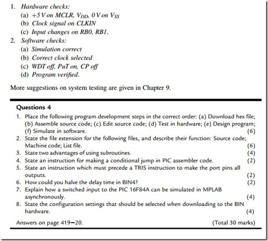
Preliminary hardware inspection and testing is important if the circuit is newly constructed, and essential if it is a new design. First, have a good look at the board to check that the correct components have been fitted in the correct places and orientation, there are no dry joints or solder bridges and so on. Connect the power before fitting the chip(s) if they are in sockets, and check that the supply voltages are correct, and on the right pins. When the hardware has been thoroughly checked, switch on and check that the MCU is not overheating.

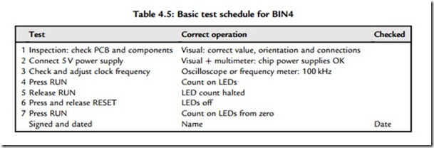
In a commercial product, a test schedule must be devised and correct operation confirmed and recorded. The test procedure should check all possible input sequences, not just the correct ones, if the design is to be completely reliable. It is quite difficult to be sure that complex programs are 100% testable, as it is often not easy to predict every possible operating sequence. An outline test procedure for BIN4 is suggested in Table 4.5.

The program should start immediately on power-up. If it does not function correctly when tested against the original specification, a fault-finding process needs to be followed, as outlined below.

PIC Microcontrollers-1172

PIC Microcontrollers-1173

1. Download the supporting documentation for MPLAB from www.microchip.com. Study the tutorial in the User’s Guide and the help files supplied with MPLAB as necessary to familiarize yourself with editing, assembling and simulating an application program. Start up MPLAB, create a source code file for BIN3, and enter the assembler code program, leaving out the comments. Assemble, correct any errors and simulate. Check that the port B (F6) file register operates as required.

2. Modify the program as BIN4, and confirm that its operation is essentially the same.

3. Modify the program to scan the output, that is, move one lit LED along the display, repeating indefinitely, using a rotate instruction.

4. Construct a prototype circuit, download BIN4 and test to the schedule given in Table 4.5.

Refer forward to Chapter 10 if necessary.

5. If Proteus VSM is available, enter or download the schematic and source code for application BIN4 from www.picmicros.org.uk. Assemble the source code, attach the hex file to the MCU and check that the simulation works (LEDs flash). Adjust the program to give an output period of exactly 50 ms at RB0. Use NOPs in the code if necessary. Use the virtual oscilloscope and timer counter to check the output period, and the logic analyzer to display all the outputs simultaneously.


PIC Program Development:Program Downloading

Program Downloading

After testing in the simulator for correct operation, the machine code program can be blown into the flash memory on the chip. The program is downloaded via a serial link into a specific pin, RB7 in the case of the 16F84A. There are two methods for program downloading, outlined below.

Programming Unit

The original programming method for PIC chips required the chip to programmed before fitting in the finished hardware circuit. A programming unit was plugged into the serial port of the PC (COM1 or COM2) and the chip inserted into the zero insertion force (ZIF) socket on the programmer (Figure 4.5). The chip orientation had to be carefully checked, as inversion would reverse the supply pins and burn out the chip. Antistatic precautions had to be observed, since the PIC is a complementary metal oxide semiconductor (CMOS) device, and static discharge on a pin can break down the field effect transistor (FET) gate insulation in the internal circuitry. Before downloading, the correct device must be selected in MPLAB under device specifications, and the configurations bits set as described below. These can also be set up using an assembler directive in the source code.

Oscillator (Clock): RC

The main options in the earlier chips were ‘RC’ and ‘XT’. RC must be selected for the oscillator configuration used in the BIN hardware. XT will be selected in later applications

PIC Microcontrollers-1170

sing an external crystal oscillator. The program will not run in the hardware if the wrong type of oscillator has been selected, so check this carefully. More recently introduced chips now have a third option, an internal oscillator that eliminates the need for external components to control the clock. This is now generally the preferred option.

Watchdog Timer: Off

The watchdog timer (WDT) is an internal timer, which automatically restarts the program if it is not cleared back to zero within 18 ms, using the instruction CLRWDT. This can be used to stop the controller hanging, owing to an undetected program bug or an input condition that has not been predicted in testing. For applications not using this feature, WDT must be switched off, or the program will reset repeatedly, preventing normal operation.

Power-up Timer: On

Mains-derived power supplies may take some time to reach the correct value (þ5 V) when first switched on. The power-up timer (PuT) is an internal timer which delays the start of program execution until the power supply is at the correct voltage and is stable. This helps to ensure that the program starts correctly every time. It is not relevant in simulation mode, but should be enabled when the program is downloaded for hardware operation.

Code Protect: Off

If the code protect (CP) bit is enabled, the program cannot be read back into MPLAB and copied or manipulated. This is normally only necessary for commercial applications to prevent software piracy, so we can switch off code protection for our simple examples.

For program downloading, PICSTART would be selected from the Programmer menu. If the programming unit had been correctly connected, a programming dialogue was displayed, with the hex code to be downloaded visible (Figure 4.6; note that this illustration dates back to version 5 of MPLAB). When the configuration bits had been checked, the Program operation could be selected to download the machine code. When complete, confirmation of successful programming should be received, and the chip manually transferred to the application circuit, again observing antistatic precautions.

In-Circuit Programming and Debugging

In-circuit programming is now usually the preferred downloading method, where the chip is left in-circuit after assembly of the printed circuit board (PCB), allowing programming and final debugging in the final hardware. When a board is produced in volume, the programming can be done as the final stage when the hardware is complete. This is also very useful at the prototyping stage, as program modifications can be more rapidly and safely implemented and tested.

PIC Microcontrollers-1171

To facilitate in-circuit programming and debugging (ICD), the board is designed with a six-pin connector, which connects the programming pins on the chip to a programmer/ debugger module that is in turn connected to the universal serial bus (USB) output on the host PC. This system has already been illustrated in Chapter 1 (Figure 1.11), and will explained in more detail in Chapter 7 by examining some Microchip demonstration systems.

When the hardware has been connected, the appropriate programmer/debugger is selected from the programmer menu. PICkit2/3 is the low-cost option, which nevertheless offers some very useful features. With the connection confirmed, the program can be downloaded. The same module can then be selected from the debugger menu and the program run and debugged using the same tools as used in software simulation (single step, breakpoints, etc.). However, program execution now takes place in the chip itself. The interaction with the real hardware can be monitored, and hence the hardware and software verified at the same time. Note that not all chips support in-circuit debugging, especially smaller and older chips. Neither the 16F84A nor the 16F690 supports ICD without a special header, which must be connected between the debugger and the chip. The PIC 16F887 used later on the Microchip 44-pin demo board does support ICD.

When debugging is complete, the final step is to configure the chip to run independently by selecting the Release option in the drop-down menu in the project toolbar. This allows the board to run when disconnected from the debugging module.

Thus, the software can be tested and debugged in stages: initially in MPSIM or Proteus VSM, and finally in the actual hardware. Proteus also provides fully featured PCB design as well as circuit simulation, so the finished hardware can be produced using the same package.


PIC Program Development:Program Simulation

Program Simulation

The BIN4.HEX file could now be downloaded to the PIC chip and the program executed in hardware. It should run correctly because the program given here is known to be good. However, when a program is first developed, it is quite likely that logical errors will be present.

PIC Microcontrollers-1166

PIC Microcontrollers-1167

This means that the program executes but it does not necessarily carry out the right operations in the right order. For example, if the wrong input pin is specified for testing, the button will not be detected. Logical errors can be detected by running the program through a test sequence that exercises all the features of the application. Any operational errors then have to be traced back to the relevant source code section. This process may have to be repeated many times, making it very time consuming.

This is where simulation is useful: it allows the program to be ‘run’ in a virtual environment on the host PC, as if it were being executed in the chip, but without having to download to the actual hardware. It can then be checked for logical errors and the source code changed and re-tested much more quickly and easily. This will allow most of the logical errors to be eliminated, leaving maybe a few issues related to the real hardware to be resolved, e.g. input/ output timing.

MPLAB provides a source code simulation and debugging for the MCU alone, while Proteus VSM provides a much more user-friendly interactive method, with an animated schematic and virtual signal analysis for the whole circuit (see Appendix E). Simulation allows the effect of the program on the registers and outputs to be checked at critical points. For example, in BIN4 we would check to see that port B has been incremented after the execution of the main loop, because this is the primary function of the program. Figure 4.4 shows a screenshot from MPLAB version 8.60 when simulating BIN4.

MPLAB now provides a logic analyzer, which allows the outputs to be viewed on a time axis, as seen in Figure 3.5 by selecting View, Simulator Logic Analyzer. The ‘Channels’ button opens a dialogue that allows the output pins RB0 to RB7 to be added to the display.

Single Stepping

Source code debugging allows the program to be tested in the edit window. First, load and assemble the source code file BIN4.ASM. Then enable simulation mode by selecting ‘Debugger, Select Tool, MPLAB SIM’. A control panel should appear in the toolbar. Operate

PIC Microcontrollers-1168

the ‘Run’ button: nothing appears to happen, but when the ‘Halt’ button is operated, the current execution point is indicated in the source code window. You may get a message about the ‘Watchdog Timer’, which is an automatic interrupt that prevents the program getting stuck in a loop. If necessary, open the Configure, Configuration Bits dialogue and turn the watchdog timer off, unchecking the ‘Configuration Bits set in code’ option. At the same time, ensure that the Power-Up Timer and Code Protection are off. These will be explained later. The program can now be executed one instruction at a time using the ‘Step Into’ button in the control panel, and the sequence examined. With no inputs, the program should loop through the reset sequence. The program can be restarted from the top at any time by clicking on the ‘Reset’ button. If Animate is selected from the Debugger menu, execution steps automatically.

Input Simulation

We now need to simulate the action of the push buttons in the hardware that are used to start and stop the output sequence. Select Debugger, Stimulus, New Workbook (Asynch tab). Clicking the first cell in the PIN/SFR column allows an input to be selected from a drop-down menu. Select RA0 in the first row, and RA1 in the second. In the Action column, set both to toggle mode: this will make the input change each time the Fire button is pressed. The inputs can now be operated to allow the program to proceed from the reset loop. Both inputs should be set high initially, simulating the default (inactive) condition in the hardware. Taking RA1 low will allow the main loop to proceed, and toggling RA0 will execute the reset loop. Unfortunately, the state of the input is not indicated in the stimulus table, so file register 05, port A, must be displayed (preferably in binary) to confirm the changes on the inputs.

Register Display

The special function registers can be viewed to check the effect of the program on the output register 06, port B. The changes at the inputs can also be checked, and any intermediate changes in internal registers tracked. Registers can also be displayed selectively using a watch window. The display format can be changed from hex to binary by right-clicking for the register properties, so individual bit status can be checked. Port A bits 0 and 1 should change with the asynchronous stimulus inputs, and port B should display a random binary number after the increment loop has been executed for an arbitrary time.

Step Out, Step Over

The Step Into control will step through all subroutines. Once the program has entered the delay loop, the same simple sequence is being repeated, so single stepping is not so useful. We need either to drop out of the subroutine (Step Out) or to bypass it altogether (Step Over). These commands cause the loop to be executed at full speed, with single stepping being resumed after the RETURN instruction. Once a subroutine is correct, it can be stepped over when debugging the rest of the program.

Breakpoints

Another technique for executing selected parts of the program at full speed is the breakpoint. For example, if part of a large program is known to be correct, we will want to run through that section at full speed and start single stepping at a later point in the program. In BIN4,

a breakpoint can be set at the start of the main loop so that it executes once, then stops so we can inspect the registers. A breakpoint can be set by simply double-clicking in the line number margin of the source code window. The program can then be run from the start, and it will stop at the breakpoint. Run again, and a complete loop will be executed at full speed and port B should be seen to increment by one.

Stopwatch

The program timing can be checked using the stopwatch feature. This displays the total number of instructions executed and the time elapsed, calculated from the simulated processor clock frequency. For BIN4, RC oscillator should be selected in the configuration dialogue. The clock speed is set in the Debugger, Settings dialogue, Osc/Trace tab. In this case, set the processor frequency to 100 kHz. Then run the program to the breakpoint at ‘start’, zero the clock and run again. The stopwatch will display the total time for one cycle. The frequency of the output can be predicted from this measurement. Two program loop cycles will cause the low-output bit RB0 to be toggled up and down once, giving one full output cycle. Therefore, we can double the loop time to give the output period, and calculate the reciprocal to give the frequency at RB0.

PIC Microcontrollers-1169

This shows that changes in the higher order output bits will be clearly visible using this clock frequency with the maximum delay loop count (FF). The frequency at RB1 will be about 8 Hz, RB2 4 Hz, RB3 2 Hz and so on, with RB7 flashing about once every 8 s. By adjusting the count value, and inserting NOP (no operation) instructions, an exact set of frequencies can be obtained. Using a crystal clock or calibrated internal clock will make the timing more accurate. More information about using MPLAB for debugging is given in Chapter 9.


PIC Program Development:Program Assembly

Program Assembly

To create the PIC program, the MPLAB IDE development system must be downloaded and installed from the Microchip website www.microchip.com. After starting the software, clicking on the new file button opens a source code edit window. The code for the demo programs can be entered and saved in a suitable folder, using the same name as the fileset,

e.g. BIN4. The source code is saved as APPNAME.ASM. If the source code already exists, it can be reopened in the usual way. The sample files may be downloaded from www.picmicros.org.uk. A workspace file will be found, BIN4.MCW, which will open all the relevant windows automatically (File, Open Workspace).

Note that in previous versions of MPASMWIN there was a limited file path length, so a folder near the root of the drive is desirable. If the file path is too long, an error message may be generated by the assembler, but it will not state the cause explicitly. This is simply a historical limitation of the assembler, but can prevent successful assembly for no obvious reason. This problem seems to have been fixed in the current version.

Once entered or opened in the edit window, the source code can be assembled in MPLAB by selecting ‘Quickbuild sourcefile.asm’ from the Project menu. The correct processor type must first be selected via the configuration menu, ‘select device’. The assembler program (MPASM) takes the source code text and decodes it character by character, line by line, starting at the top left. The corresponding machine code for each line in the source code is generated until the END directive is detected. The binary code created is automatically saved as a file called BIN4.HEX in the same folder as the source code. At the same time, several other files are also created, some of which are needed for debugging.

In Proteus VSM, the circuit schematic must be created first, and then the program attached to the MCU, by selecting Source, Add/Remove Source Files from the menu. The processor type and assembler must be selected and a New source file created or attached. The program is assembled by selecting Build All in the Source menu, and is automatically reassembled after editing when the simulator is set to run, which makes source code debugging quick and easy. Application creation in Proteus VSM is detailed in Appendix E.

Syntax Errors

If there are any syntax errors in the source code, such as spelling, layout, punctuation or failure to define labels properly, error messages will be generated by the assembler. These will be displayed in a separate window, indicating the type of error and line number. The messages and line numbers must be noted, or the error file, BIN4.ERR, printed out then the necessary changes made to the source code. The error is sometimes on a previous line to the one indicated, and sometimes a single error can generate more than one message. Warnings and information messages can usually be ignored, and can be disabled. There are more details about error messages in Chapter 9.

You may receive the following messages:

PIC Microcontrollers-1164

The first warning is caused by the special instruction TRIS, which is not part of the main instruction set. It is a simple way of initializing the port, and there is an alternative method using register bank selection, which is preferred in real applications. This will be introduced later.

The message about the ‘default destination’ is caused by the simplified syntax used in these programs, where the file register is not explicitly specified as the destination in instructions where the result can be placed in either the file register or the working register. The assembler assumes that the file register is the destination by default, and we are taking advantage of this to simplify the source code.

When all errors have been eliminated and the program has been successfully assembled, the machine code can be inspected by selecting ‘View’, ‘Program Memory’. Note that the source code labels are not reproduced, as the program code has been ‘disassembled’ (recreated) from the machine code. That is, the hex file has been converted back to mnemonic form so that it can be checked against the original.

List File

A program ‘list file’ BIN4.LST is produced by the assembler, which contains the source code, the machine code, error messages and other information all in one listing (Table 4.4). This is useful for analyzing the program and assembler operations, and debugging the source code.

The list file header shows the assembler version used and source file details. The column headings are:

LOC: memory location addresses at which the machine code will be stored VALUE: the numerical value with which equate labels will be replaced OBJECT CODE: machine code produced for each instruction

PIC Microcontrollers-1165

Note that no machine code is produced by lines that are occupied by a full line comment. The actual program starts to be produced at line 00041. The machine code for the first instruction is shown in column 2 (3000), and the address where it will be stored in the chip when downloaded is shown in column 1 (0000). The whole program will occupy locations 0000 to 000F (16 instructions).

If we study the machine code, we can see how the labeling works; for example, the last instruction ‘GOTO start’ is encoded as 2808, and the 08 refers to address 0008 in column 1, the location with the label ‘start’. The assembler program has replaced the label with the corresponding numerical address for the jump destination. Similarly, the label ‘porta’ is replaced with its file register number 05 in the instruction code to test the input, 1C05.

The label values are listed again in the symbol table. These values will be used by the simulator to allow the user to display the simulated registers by label. The amount of program memory used, 16 locations, 0000 to 000F, is shown in graphical format in the memory usage map, and finally a total of errors, warnings and messages given. If there are fatal errors, which prevent successful assembly of the program, the list file will not be produced.


PIC Program Development:Program Analysis

Program Analysis

The program BIN4 will now be analyzed in some detail as it was designed to contain examples of common PIC syntax. A sample instruction of each type will be examined.

PIC Microcontrollers-1160

PIC Microcontrollers-1161

The use of labels in place of numbers makes programs easier to write and understand, but we have to ‘declare’ those labels at the beginning of the program. In assembly code, the

PIC Microcontrollers-1162

assembler directive EQU is used to assign a label to a number, which can be a literal, a file register number or an individual register bit. In BIN4, ‘porta’ and ‘portb’ are the port data registers (05 and 06) and ‘timer’ is the first spare register (0C), which will be used as a counter register. The labels ‘inres’ and ‘inrun’ will represent bit 0 and bit 1 of port A; they are simply given the numerical values 0 and 1. The label is replaced by the number when the program is assembled.

Port Initialization

TRIS portb

Port B is used as the output for the 8-bit binary count. The data direction must be set up using the TRIS command, which loads the port data direction register with the data direction code. In this example, the code is given in binary, b‘00000000’. This is useful, especially if the port bits are to be set as a mixture of inputs and outputs; the binary code identifies the data direction for each bit individually. This code is loaded into W using MOVLW, and the TRIS command follows.

The TRIS instruction is still available as a simple way of initializing the ports, but the manufacturers recommend an alternative method, which involves bank selection, and will be covered later. Hopefully, TRIS will continue to be supported in by the MPASM assembler, as it is easier for beginners.

Program Jumps

GOTO start

The ‘GOTO label’ command is used to make the program jump to a line other than the one following. In BIN4, ‘GOTO reset’ skips over the following DELAY routine, to start the main loop. We will come back to the reason for this in a moment. There is another unconditional jump at the end of the program, ‘GOTO start’, which makes the main loop repeat endlessly. Other ‘GOTO label’ instructions are used with ‘Test and Skip’ instructions to create conditional branches. In this program, the input buttons are checked using this type of instruction and the program branches, or not, depending on whether a button has been pressed.

Bit Test and Skip if Set/Clear

BTFSS porta,inres

The input button connected to port A, bit 0 is tested using the above instruction, which means ‘Bit Test File (register bit) and Skip the next instruction if it is Set (¼1)’. Without labels, the instruction ‘BTFSS 05,0’ would have the same effect. The buttons are connected ‘active low’, meaning that the input goes from ‘1’ to ‘0’ when the button is pressed. If the button connected to RA0 is not pressed, the input will be high, that is, set. The following instruction, ‘GOTO reset’ will therefore be skipped, and the next executed. When the button is pressed, the ‘GOTO reset’ is executed, and the CLRF instruction repeated, clearing the previous count.

BTFSC means ‘Bit Test and Skip if Clear’; it works in the same way as BTFSS, except that the logic is reversed. Thus, ‘BTFSC porta,inrun’ tests bit 1 of port A register and skips the following ‘GOTO start’ if the ‘run’ button has been pressed. The program will then proceed to increment the output count. If the button is not pressed, the program

waits by jumping back to the ‘start’ line. The combined effect of the input buttons is that the count runs when the ‘run’ button is pressed, and the count is reset to zero if the ‘reset’ button is pressed.

Decrement/Increment Register and Skip If Zero

DECFSZ timer

The other instructions for conditional branching allow a register to be incremented or decremented and then checked for a zero result, all in one instruction. This is a common requirement for counting and timing applications, and in the delay routine in BIN3, a register ‘timer’ is loaded with the maximum value FF and decremented. If the result is not yet zero, the jump ‘GOTO down’ is executed. When the register reaches zero, the GOTO is skipped and the subroutine ends. In BIN4, the timer value is set up before the delay subroutine is called.

Subroutine Call and Return

The main elements of the subroutine call structure are shown below:

PIC Microcontrollers-1163

In this program, the subroutine provides a delay by loading a register and counting down to zero. The delay is started using the ‘CALL delay’ instruction, when the program jumps to the label ‘delay’ and runs from there. CALL means ‘jump and come back to the same place later’, so the return address has to be stored for later recall in a special memory block called the ‘stack’.

The address of the instruction following (in this case ‘GOTO start’) is saved automatically on the stack as part of the execution of the CALL instruction. The subroutine is terminated with the instruction ‘RETURN’, which does not require an operand because the return destination address is automatically pulled from the stack and replaced in the program counter. This takes the program back to the original place in the main program. The PIC 16 stack can store up to eight return addresses, so multiple levels of subroutine can be used. The return addresses are pushed onto and pulled from the stack in order, so if a CALL or RETURN is missed out of the program, a stack error will occur. Unfortunately, this mistake will not be detected by the assembler, but will cause a run-time error message.

End of Source Code

END

The source code must be terminated with assembler directive END so that the assembly process can be stopped in an orderly way, and control returned to the host operating system. It is the only assembler directive that is essential.


PIC Program Development:Program Editing

Program Editing

The program is written using the instruction set of the processor selected, as specified in the MCU data sheet. The instruction set is essentially the same for all 16 series PIC chips. The source code, that is, the assembly code program, must be entered into a suitable text editor, which is normally provided with the development system. We will not go into the details of using a text editor, as it is assumed that the reader is familiar with using a word processor.

The MPLAB programming window has limited editing features, because it is only used for creating plain text files. The typeface Courier is used because each character occupies the same space, unlike proportionally spaced typefaces such as Arial and Times Roman. Displayed in this way, the text lines up vertically as well as horizontally, so the program can be laid out consistently in columns using tab stops, making it easier to understand. The tab spacing should be set to eight characters for the programs in this book. When printing, also use Courier to maintain the correct layout.

When a new application is started, a separate folder should be created to contain the source code file, and all the other files that will be generated by the assembler. Name the folder with the application name, e.g. BIN3. When the source code file has been opened, enter the source code filename (e.g. BIN3.ASM) at the top of the file, and immediately save it in the folder. This ensures that the required filepath is checked for correct operation before any further source text is entered. Always keep a backup copy of your file on a different drive before quitting the development system.

Instruction Set

The PIC 16 data sheets and the mid-range manual show the instruction set arranged by byte, bit, literal and control operations. Table 4.2 shows the same instruction set organized by function with an example given with each instruction so that the typical syntax can be seen. A detailed description of each instruction is provided in the data sheet, with more information in Chapter 6.

The grouping of the instructions in Table 4.2 reflects the different types of instruction explained in Chapter 2: data movement, single and register pair arithmetic and logical operations, sequence control and miscellaneous instructions. In the example instructions, the register used is always 0C, the first general purpose register in the smaller PIC 16 chips. The register being operated upon will normally be referred to by label (see Program BIN3 below). Literals and register bit numbers may be referred to by number or label, depending on the context.

BIN3 Source Code

Program BIN3 uses the same instructions as BIN2 (Chapter 3), with additional statements to read the switches and control the output. Program 4.1 is the result.

First, note the general layout and punctuation. The program header block contains as much information as is necessary at this stage. These comments are preceded by a semicolon on each line to indicate to the assembler that this text is not part of the program. Assembler

PIC Microcontrollers-1157

PIC Microcontrollers-1158

directives such as EQU and END are also not part of the program proper, but used to define labels and the end of the program source code. The labels ‘porta’, ‘portb’ and ‘timer’ refer to file registers 05, 06 and 0C, respectively; ‘inres’ and ‘inrun’ are input bit labels representing the push buttons. The program uses ‘Bit Test and Skip’ instructions followed by ‘GOTO label’ for conditional jumping.

At this stage, the learner can type the source code into the editor without full analysis in order to practice use of the editor. The instructions are placed in the first three columns, and the comments can be left out to save time. Labels go in the first column, instruction mnemonics in the second and the instruction operands in the third. The source code text file should be saved as BIN3.ASM in a suitably named directory or folder on disk. Alternatively, the source code file can be downloaded from the support website www.picmicros.org.uk. It can then be tested in the free MPLAB simulator (see Section 4.7) or in Proteus VSM (see Appendix E).

Syntax

‘Syntax’ refers to the way that words are put together to create meaningful statements, or a series of statements. In programming, the syntax rules are determined by the assembler,

which will be used to create the machine code. The assembler must be provided with source code that it can convert into the required machine code without any ambiguity, that is, only one meaning is possible. This is why the assembler syntax rules are very strict.

Layout

The program layout should be in four columns, as described in Table 4.3. Each character then occupies the same space, and the columns are correctly aligned. The label, command and operand columns are set to a width of eight characters, with the maximum label length of six characters, leaving a minimum of two clear spaces between columns (longer labels can be used, but a different form of the program layout must then be used). The tab key is normally used to place the text in columns, and the tab spacing can be adjusted if necessary.

PIC Microcontrollers-1159

a semicolon on any line of code helps the programmer and user to understand the program. It has no effect on the operation of the program. Full line comments may also be used between program blocks

Comments

Comments are not part of the actual program, but are included to help the programmer and user understand how the program works. Comments are preceded by a semicolon (;),

which can be placed at the beginning of a line to indicate a comment which relates to a whole program block (functional set of statements), or at the start of column 4 for line comment. The comment and line are terminated with a line return (‘Enter’ key).

A standard header block is recommended (see Program 4.1). For simple programs, the first line should at least contain the source code file name, the author and date, and/or version number. A program description should also be provided in the header, and for programs that are more complex, the processor type, target hardware details and other relevant information. In general, the bigger the program, the more information would be expected in the header comments.


PIC Program Development:Program Structure

Program Structure

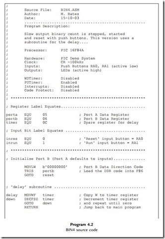
Structured programming means constructing the program, as far as possible, from discrete blocks. This makes the program easier to write and understand, more reliable and easier to modify at a later date. Program BIN3 is unstructured, in that the program instructions are essentially executed in the order given in the source code. An equivalent ‘structured’ program, BIN4, is listed as Program 4.2.

The main difference between BIN3 and BIN4 is that the program now has the delay sequence as a ‘subroutine’. The subroutine is inserted before the main program block, and assembled first. It is then ‘called’ from the main program by label. The subroutine can be created as a self-contained program block, and reused in the program as necessary. It can be called as many times as required, which means that the block of code needs to be written only once. It can also be converted to a separate file and reused in another program. In addition, the delay time is loaded before the subroutine execution, so the same delay routine could be used to provide different delay times.

A program flowchart has been given for BIN3 (Figure 4.2). The same flowchart describes BIN4, but the delay routine can now be expanded as a separate subroutine flowchart

(Figure 4.3). The use of flowcharts in program design will be more fully examined in Chapter 8.