PIC Development Systems:Hardware Test

Hardware Test

When simulating correctly, the program can be downloaded. The PICkit programmer is plugged into a USB port and Programmer, Select Programmer, PICkit2 from the menus. Successful connection to the programmer should be confirmed in the output window. Sometimes an updated version of the programmer operating system needs to be downloaded. A programming toolbar also appears.

Assuming the source has been successfully assembled into program memory (View, Program Memory), download it by hitting ‘Program the Target Device’ button, and run the program using the ‘Bring Target Device MCLR to Vdd’ button. The LEDs on the LPC board should start scanning, and the speed should be controlled by the on-board pot. Note that the SW1 push button on the board has no effect as it is overridden by MCLR from the programmer.

Thus, the LPC board provides a convenient demonstration of all the main features of PIC program development, except for ICD.


PIC Development Systems:PIC 16F690 Chip

PIC 16F690 Chip

The data sheet for this chip should be downloaded from www.microchip.com and studied in conjunction with this section. The pin-out can be seen in the schematic Figure 7.3; it has only 20 pins in total, hence the ‘low pin count’ description. The 16F690 is representative of the 16 series chips as it has a typical range of interfaces, including:

• Digital input/output

• Analogue inputs (12)

• Multi-mode timers (3)

• Serial ports (USART, SPI, I2C)

• An internal clock oscillator (4 MHz).

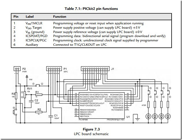
The chip has 4k of program memory, with 256 bytes each of random access memory (RAM) and electrically erasable programmable read-only memory (EEPROM). It can be initialized to provide simple digital input/output (I/O) on 18 of the 20 pins, which are grouped as ports A (6), B (4) and C (8). Notice that port bits RB0 to RB3 are missing, and the chip is programmed via RA0 and RA1. In common with most current chips, the 16F690 has analogue inputs, which allow voltage measurement interfaces to be connected. The basic setup will be explained here, and there is further information on the principles of analogue to digital conversion in Section 12.3.3 (Chapter 12). For digital I/O the ports must be initialized as shown in the test program below because the analogue pins default to analogue inputs if not explicitly set up.

The analogue inputs use a single analogue to digital (A/D) converter, which can be connected to any one of 12 input pins (AN0 to AN11) via a multiplexer. The A/D converts an input voltage to a corresponding 10-bit binary code, which is placed automatically in special function registers (SFRs) ADRESH and ADRESL when the conversion is finished. The conversion is triggered by setting bit ADCON0,1 (A/D control register 0) and is complete when the same bit is set low by the hardware. This bit can be polled (checked repeatedly in a loop) or an interrupt set to indicate completion.

An alternative method of checking an analogue input is to use a comparator, which simply indicates which of two inputs is at a higher voltage (the input polarity). The analogue comparator has two inputs, labeled plus (þ) and minus (-). Signals are applied to both, and the output goes logic high if the voltage at the (þ) input is higher than at the (-) input, otherwise it is low. In the 16F690, several inputs are multiplexed with reference voltages so different combinations of inputs can be detected (see data sheet).

The hardware timers can be used in the usual counter or timer mode, but in addition can be used in capture, compare or pulse width modulation (PWM) mode. Capture means the timer value is stored when a selected input changes, allowing, for example, the period of an input to be measured. Compare mode is the inverse operation: the timer value is compared after each increment to a reference register and an output changed or interrupt generated when they match. This can be used to generate an output pulse waveform of a set period. PWM is similar, designed to provide a pulse waveform with a set mark/space (high/low) ratio.

Serial ports allow communication with other devices (microprocessors or computers) via single- or two-wire connection. There are various methods (protocols) available; the 16F690 supports RS232, RS485, LIN, SPI and I2C. The function of each pin must be selected during

initialization, since each has multiple operating modes. The internal clock frequency is selected in the OSCCON register. The internal clock defaults to a frequency of 4 MHz, with 8 MHz the maximum. The default is accepted in the test program.

All the peripheral interfaces mentioned here are explained further in Chapter 12, and typical applications are described in detail in Interfacing PIC Microcontrollers: Embedded Design by Interactive Simulation (Newnes 2006) by this author.


Programming Techniques:Data Table

Data Table

A program may be required to output a set of predefined data bytes, for example, the codes to light up a seven-segment display with the correct pattern for each display digit.

The data set can be written into the program as a table within a subroutine, and the data list accessed using CALL and RETLW. To fetch the table value required, the position in the table is placed in W. ‘0’ will access the first item, ‘1’ the second and so on. At the top of the subroutine, ADDWF PCL is used to add this table pointer value to the program counter register so that the execution point jumps to the required item in the list.

RETLW is then used to return the table value in W, and it can then be moved to the required file register.

Program 6.6, TAB1, shows how such a table may be used to generate an arbitrary sequence at the LEDs in our BIN demonstration hardware. In this case, it is a bar graph display, which lights the LEDs from one end, using the binary sequence 0, 1, 3, 7, 15, 31, 63, 127, 255.

GPRs labeled ‘timer’ and ‘point’ are used. Port B is set as outputs, and subroutines are defined for a delay and to provide a table of output codes. In the main loop, the table pointer register ‘point’ is initially cleared, and will then be incremented from 0 to 9 as each code is output. The value of the pointer is checked each time round the loop to see if it is 9 yet. When 9 is reached, the program jumps back to ‘newbar’, and the pointer is reset to zero.

For each output, the pointer value (0e8) is placed in W and the ‘table’ subroutine called. The first instruction, ‘ADDWF PCL’, adds the pointer value to the program counter. At the first call, this value is zero, so the next instruction, ‘RETLW 000’, is executed. The program returns to the main loop with the value 00 in W. This is output to the LEDs, the delay is run, and the pointer value incremented. The new value is tested to see if it is 9 yet, and if not, the next call is made to the table, until finally the ninth code (0FF) is returned to the main output loop for display. After this, the test of the pointer being equal to 9 succeeds, the jump back to ‘newbar’ is taken, and the process repeats. Note the use of ‘W’ as the destination for the result of the subtract (SUBWF) instruction. This is necessary to avoid the pointer value being overwritten with the result of the subtraction.

PIC Microcontrollers-1220

For full details on topics in this chapter related to the assembler, refer to the ‘MPASM User’s Guide’ at www.microchip.com.

1. State (a) the number of clock cycles in a PIC instruction cycle, and the number of

instruction cycles taken to execute the instructions (b) CLRW and (c) RETURN. (3)

2. If the PIC clock input is 100 kHz, what is the instruction cycle time? (2)

3. Calculate the preload value required in TMR0 to obtain a delay of 1 ms between the load operation and the T0IF going high, if the clock rate is 4 MHz and the prescale

ratio selected is 4:1. (3)

4. List the bits in the SFRs that have to be initialized to enable an RB7:RB3 interrupt. (2)

5. State one advantage each of the RC, X T, HS and INTOSC clock options. (4)

6. State the assembler directive that must be used in all PIC programs. (2)

7. Explain the difference between a subroutine and a macro, and one advantage of each. (4) Answers on pages 420e1. (Total 20 marks)

1. Calculate the time taken to execute one complete cycle of the output obtained from TAB1 with a clock rate of 100 kHz. Check this result by simulation.

2. Modify the program TIM1 to use a timer interrupt rather than polling to control the delay.

3. Devise a program to measure the period of an input pulse waveform at RB0, which has

a frequency range of 10e100 kHz. When measured, the input period should be stored in

a GPR called ‘period’ as a value where 0A16 ¼ 10 ms and 6416 ¼ 100 ms (resolution of 1 bit per microsecond). The MCU clock frequency is 4 MHz.


More PIC Microcontrollers:Serial Ports

Serial Ports

Serial communication ports allow the PIC to communicate with other MCUs, or exchange data with a master controller, via a single connection. Serial connections may also be made with external memory devices and sensors. There are several protocols available in PICs:

• USART (universal synchronous asynchronous receiver transmitter)

• SPI (serial peripheral interface)

• I2C (inter-integrated circuit)

• LIN (local interconnect network)

• CAN (controller area network)

• Ethernet

• USB (universal serial bus)

USART

RS232 is an asynchronous communication protocol previously used in the serial (COM) port of the PC for connecting peripherals such as the mouse, before USB was developed. It is low speed, but easy to understand, and has been used as the direct communication between computers, terminals and other systems for many years. It is also still used to download programs to the PIC MPSTART programmer module.

‘Asynchronous’ means that no separate clock signal is provided with the data, so correct reception of data relies on the sender and receiver operating at the same speed, with reception synchronized using a start bit for each byte. Serial data is sent and received as individual bytes using a pair of shift registers (Figure 12.7a). After each bit is shifted out of the send register onto the line, it must be shifted into the receiver register at the same time. In other words, the receiver must sample the line during the time that the transmitted bit is present. It must then take the next sample after the appropriate interval, which depends on the data rate.

PIC Microcontrollers-1310

The ‘baud rate’ sets this time interval, and there is a set of standard rates of between 300 and 115 200 bits per second. The sender and receiver must be initialized to operate at the same baud rate. At a typical rate of 19 200 baud (about 20 kbits/s), the bit time interval is about 50 ms. The signal is illustrated in Figure 12.7(b). The line is high when inactive; the start of a byte is indicated by the falling edge of a start bit. The receiver then samples the line at the required interval to read each bit, and the sampling is retriggered at the start of each byte.

When the USART is operated in asynchronous mode (Figure 12.8), there is a separate data path for send (TX) and receive (RX). One byte of data is transmitted at a time down the serial line, with start, stop and optional error check (parity) bits. If an error is detected, a retransmission can be requested. A synchronous mode is also available, when the TX pin is used instead to

PIC Microcontrollers-1311

carry a clock (CK) signal. This is sent alongside the data signal to clock the receiver, making the process more reliable. In this mode, the device can still send and receive, but only in one direction at a time.

The RS232 data signal produced by the PIC USART is output at TTL (transistoretransistor logic) levels. Most terminals, such as the PC, will produce a signal that is transmitted at higher bipolar voltage, typically ± 12 V, to allow the signal to travel further on the line (up to about 100 m). If the PIC is to communicate with such a terminal, the signal must be passed through a line driver, which will boost the voltage and shift the level as required.

SPI Bus

The SPI system uses three pins on each system device:

• Serial data out (SDO)

• Serial data in (SDI)

• Serial clock (SCK).

It is a single-master, multi-slave system, using hardware slave selection (Figure 12.9). To exchange data with a slave, the master selects it by taking the slave select input low (!SS). Synchronous 8-bit data is then exchanged via SDI or SDO, with a clock pulse to strobe in each bit to the destination register. Owing to the hardware selection requirements, this system is most suitable for communication between devices on the same board. Data can be transmitted and received at the same time, at a clock rate of up to 5 MHz with a 20 MHz chip clock.

I2C Bus

The I2C (pronounced eye squared see) system needs only two pins on each system device:

• Serial data (SDA)

• Serial clock (SCL).

This system also uses synchronous mastereslave communication, but with a software- rather than a hardware-based addressing system (Figure 12.10). As in a network, the destination address is transmitted on the same line (SDA) before the data. A 7- or 10-bit address can be used (up to 1023 slaves), which must be preprogrammed into an address register in each slave. The slave then only picks up the messages with its own address. The clock can operate at up to 1 MHz. I2C is suitable for communication between separate microcontroller boards, since no slave selection hardware connections are needed. Compare with SPI, the hardware is simpler, but the software is more complex. Note that in the hardware diagram, the lines are pulled up to þ5 V, giving active low, wired-OR operation on the serial bus and clock line.

PIC Microcontrollers-1312

LIN Bus

The LIN bus is a mixture of the I2C and RS232 protocols (Figure 12.11). The PIC interface is designated EUSART (extended USART) to indicate that it supports this additional bus option. It is a single-master, multi-slave protocol using a single bidirectional signal wire operating at 9e18 V (12 V) with open collector output bus transceivers and pull-up resistors. The transceivers are connected to the TX and RX pins as per RS232. Data and control bytes are transmitted in asynchronous mode with start and stop bits in the same way as RS232, but sent as message blocks with synchronization, identifier and up to 8 bytes of data, and terminated by an error check byte in the same way as a network data frame. It is primarily designed for automotive systems, where a reasonably simple and robust protocol is needed to integrate distributed controllers into a network. See Microchip Application Note AN729 for details.

CAN Bus

The CAN system (Figure 12.12) is also designed for transmitting signals in electrically noisy environments, such as motor vehicle control, using differential current drivers operating at 5 V. It is a multi-master system, meaning that any of the system nodes (electronic control units) can send a message at any time. This consists of a data frame containing identifier bits, up to 8 data

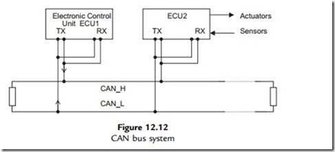
PIC Microcontrollers-1313

PIC Microcontrollers-1314

bytes, error checking and acknowledge bits. Collisions are resolved by each message having a priority code within its identifier code. CAN bus is only currently available in selected high-performance PIC 18 series devices.

Ethernet and USB

Ethernet and USB interfaces are now being added to some of the more powerful PIC MCUs, so they can be connected directly to standard peripherals. Some PIC32 (32-bit) devices support 100 Mb/s Ethernet, PIC24 (16-bit) chips do not, while some PIC18 (8-bit) chips offer 10 Mb/s Ethernet. All groups include chips with a USB 2.0 interface. Both interfaces require significant additional hardware and firmware capabilities to support these complex communication protocols.

More details on these communication interfaces is provided in Interfacing PIC Microcontrollers: Embedded Design by Interactive Simulation (Newnes 2006) by this author.

1. Summarize the key differences between the PIC 10, 12, 16 and 18 series of microcontrollers. (16)

2. State two advantages of in-circuit serial programming. (4)

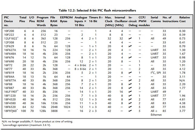
3. From the table of PIC flash microcontrollers (Table 12.2), select for minimal cost and name:

(a) a device that has eight analogue inputs in the smallest package

(b) a device that could control two PWM motor outputs, has EEPROM, runs at 40 MHz and can be programmed in C. (4)

4. Explain the essential difference between capture and compare timer operations. (3)

5. Describe the essential difference between SPI and I2C addressing. Which has more complex hardware requirements? (3)

1. Download the data sheet and study the summary page for the PIC 12F675, 16F690 and 18F8720. Summarize the features of each, and suggest a typical application for each device.

2. A robot has four axes to be controlled by a PIC MCU. Each has a PWM speed controlled motor and an incremental encoder with three digital outputs providing the position feed- back. A block of EEPROM is needed to store up to 128 programmed positions, requiring

a 16-bit code for each axis for each position. Select the most suitable chip from the Microchip website that could be used as a controller for the robot positioning system. Download the data sheet and draw a block diagram for the system, identifying the pins that should be connected to the motors and encoders. Outline how the controller will move the robot between programmed positions. Refer back to Chapter 11 if necessary.

3. Sketch a block diagram for an alternative implementation of the robot controller in Activity 2 above, using a separate controller for each axis connected to a master SPI controller. Select suitable chips for the master and slave controllers, and list the connections required. Compare the cost of each system and suggest an advantage of the mastereslave system over the single controller solution proposed in Activity 2.


PIC Development Systems:In-Circuit Programming

In-Circuit Programming

MPLAB IDE and a hardware programmer are the essential components of the Microchip toolset. Originally, PIC® chips had to be removed from the circuit for programming in a separate module, and then replaced in the target application board. Now, in-circuit programming allows the chip to be programmed without being removed, which avoids possible mechanical (broken/ bent legs) and electrical (static) damage. The MCU must incorporate the necessary hardware features to support this option. If in-circuit debugging (ICD) is supported by the design of the target hardware (six-pin connector and suitable connections to the MCU), the programming module can act as both a programming and a debugging interface.

The connections shown in Figure 7.1 are common to the low-price PICkit2/3 and the ICD2/3 programmer/debugger modules. Each has a six-pin connector, with the PICkit using a single in-line (SIL) connector on the target board. The program is downloaded via ICSPDAT/PGD (in-circuit serial programming data) synchronized by ICSPCLK/PGC (clock). If the target board does not need too much current, it can be powered from the host computer via the universal serial bus (USB) programming module (VDD and VSS). For example, the PIC 16F690-based low- pin count (LPC) demo board can be programmed without an external supply. The target board reset can be controlled from MPLAB (!MCLR) and VPP provides the programming voltage.

If the chip and development system support ICD, the same MPLAB simulation tools can be used to test the program as it runs in the actual chip, with the real hardware providing the inputs and outputs. This allows the interaction with the target hardware to be examined more closely and a final debugging stage implemented to ensure correct operation of the MCU in the actual

PIC Microcontrollers-1221

circuit. All the usual techniques are available: single stepping, breakpoints, register monitoring and so on. The finished program can then be run at full speed in the target hardware, and any final bugs removed that become apparent. Previously, an expensive in-circuit emulator would have been needed for this type of testing.

Unfortunately, the 16F690 chip does not support ICD without a header. If this feature is required, the 44-pin demo board with the 16F887 chip on board is available, since this chip contains the ICD interface while the 16F690 does not.


PIC Development Systems:PICkit2 Demo System

PICkit2 Demo System

The PICkit2 is an in-circuit programming module that supports a full range of PIC microcontrollers. PICkit3 is now available. The PICkit2 Starter Kit also includes the LPC board incorporating the 16F690 MCU and some minimal test circuitry (Figure 7.2). The programmer is connected to the USB port of the host PC running MPLAB, with the six-pin in-line output plugged into a six-pin male connector on the target board. The connections are shown in Table 7.1.

The board has four light-emitting diodes (LEDs) to display programmed output sequences, a push button connected to !MCLR and a small pot providing an analogue test input. The LPC board can be powered from the USB port via pins 2 and 3. For programming, þ12 V is applied to pin 1, but after programming is complete, it reverts to the reset (!MCLR) input function. When under control of the host PC, the on-board reset button is overridden by a command/button in the MPLAB toolbar. When detached from the programmer, the push button can be configured as a reset input or as a digital input. Pins 4 and 5 carry the program data and clock, which write the code into program memory in the target chip. Pin 6 is available for additional functions of the programmer. These features can be seen in the schematic for the LPC (Figure 7.3).

PIC Microcontrollers-1222

The board has additional connections to all the chip pins and a small prototyping area, which can be used to add peripheral components. Links are provided in the LED circuits so that they can be disconnected if these outputs are needed for another load. When the board is removed from the programmer, it needs to be connected to an external supply via connector P2.


More PIC Microcontrollers:Peripheral Interfaces

Peripheral Interfaces

In the block diagram of each chip, the peripherals are shown as separate blocks attached to the internal data bus. These provide additional features such as timers, analogue inputs and serial ports. These are set up for use by initializing the related SFRs. The appropriate combination of peripherals is a major factor in chip selection.

Timers and CCP

Hardware timers are used for timing and counting operations, allowing the processor to carry on with some other process while the timer process runs. Basic timer operation has been described in Chapter 6, where a clock input drives a counting register to measure time or count external events. Its functionality can be extended by using additional registers to store timer values, creating a CCP module. CCP stands for capture/compare/PWM.

Capture mode provides input interval measurement (Figure 12.4a). The value in a timer register is captured (stored) when an input changes; the time between the timer start and input change is therefore recorded. In the motor application, for example, the timer could be started when a pulse is received from the shaft sensor, and the time captured when the next pulse arrives, giving the period of the shaft sensor pulse. An interrupt can be enabled to signal this event.

Compare mode provides output interval generation (Figure 12.4b). A value is loaded into a register, which is then continuously compared with a timer register as it runs. When the register values match, an output pin is toggled and an interrupt generated to signal the timeout event. This is a convenient way to generate a timed interval, so that, for example, an output pulse waveform can be generated with set pulse period.

PIC Microcontrollers-1307

PIC Microcontrollers-1308

In PWM mode, preset values are loaded into two registers representing the mark and space period of the PWM output required (Figure 12.5). The timer value is then compared with the mark register and the output toggled after the mark value is reached. The timer is then restarted and compared with the space value as it runs, and the output toggled when the space value matches. The process is repeated, causing the output from the flip-flop to toggle after each mark and space interval, generating a PWM output.

Analogue Comparators

The comparator allows one voltage to be compared with another, and sets or clears its output bit depending on the polarity of the input. Many PICs incorporate comparator inputs as well as analogue/digital (A/D) inputs, with the result bits recorded in a relevant SFR. Often, there are multiple inputs which can be set up to operate in different combinations, and also trigger a range of output events, such as an interrupt. See, for example, the block diagram of the 16F690 C1 comparator module (Figure 8-2 in the data sheet).

Analogue/Digital Inputs

The analogue inputs are used in control systems with input sensors that produce a voltage, current or resistance change in response to an environmental variation or system measurement. For example, in the LPC board, a pot is connected to RA0, which is designated AN0 when used as an analogue input. In the test program, it reads 0e5 V from the pot and uses this value to control the speed of the LED output scan, by copying it into the delay counter as the initial value. The temperature controller described in Chapter 13 is designed to accept inputs from temperature sensors which give an output change of 10 mV/oC. The PIC then operates outputs to a heater or a cooling fan, which keep the temperature in the target system constant.

Most PICs provide 10-bit conversion. This means that the input voltage is converted to a 10-bit number, giving a resolution of 1 in 1024, or better than 0.1%. This is good enough for all but the most demanding applications. If the full resolution is not required, an 8-bit result can be used by ignoring the two extra bits. Multiple analogue inputs are usually available; the PIC 16F690 has 12 (AN0 to AN11). Code for performing the analogue input conversion is given in the LPC Program 7.1.

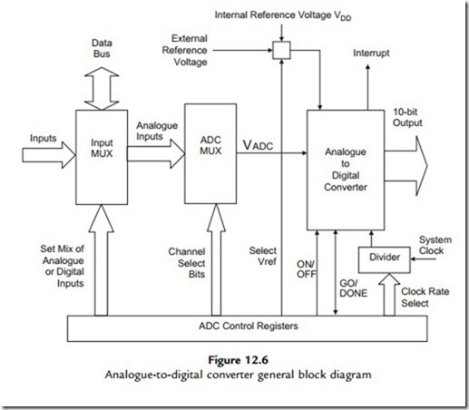
The analogue-to-digital conversion (ADC) system is illustrated in Figure 12.6. The port containing the ADC inputs can be set up with a combination of analogue and digital inputs, or all analogue. One of the analogue inputs is selected at a time for conversion, and the converter output is stored in an ADC result register. The maximum voltage level to be converted (reference voltage) can be set externally, or the internal supply voltage (þ5 V) can be used. In the temperature controller board, an external voltage reference of þ2.56 V is used, because this gives a convenient 0.01 V per bit conversion for an 8-bit result. The converter is driven by the chip clock, but a divider must be set up to allow the minimum specified conversion time (about

PIC Microcontrollers-1309

20 ms); for example, if the chip clock is 20 MHz, divide by 32 must be selected, and at 4 MHz, divide by 8. The GO/DONE bit in the control register is used to start a conversion; the same bit indicates when the conversion is finished.

The ADC works by successive approximation, details of which can be found in standard electronics references. The converter consists of a register, a digital-to-analogue converter (DAC) and an analogue comparator. The register is loaded with the half-range value (512 for 10 bits) and this is converted to an analogue value by the DAC, whose maximum output is set by the ADC reference voltage. The DAC output voltage is compared with the input, and if the input is higher, the comparator value is increased by half of the remaining range (512 þ 256 ¼ 768, set bit 8). The input is compared again and the register value adjusted up or down, until the value converges on the actual input value within 10 iterations.


More PIC Microcontrollers:Power Consumption

Power Consumption

Power consumption is generally proportional to clock speed in complementary metal oxide semiconductor (CMOS) devices, since most of the power is consumed when the transistors switch on and off. This is illustrated by the current consumption curve for a typical device, shown in Figure 12.2. For external crystal operation at clock frequencies between 4 and 20 MHz, high-speed (HS) mode must be selected when programming the chip, and below 4 MHz crystal (XT) mode. The power consumption at high speed may necessitate additional cooling measures to keep a chip within its temperature limits, especially in the larger PICs. A heat sink or even a fan, as found on the processor in a typical PC motherboard design, could be

PIC Microcontrollers-1305

used. For this reason, a major development effort has recently been applied to reducing power consumption. Extreme-low-power (XLP) devices now operate at low supply voltage (3 V) for battery-powered operation, with a typical battery life of 8 years being claimed. Judicious use of sleep and wake-up modes is also important in minimizing power consumption.

Packaging

Some sample integrated circuit (IC) packages are shown in Figure 12.3. The traditional package for integrated circuits is the plastic dual in-line (PDIP) chip, which has two rows of pins spaced at 0.1 inch intervals. The maximum number of pins that can practically be accommodated in this type of package is 64, so other formats have been adopted for larger

PIC Microcontrollers-1306

chips, and to reduce the board area consumed. The plastic leaded chip carrier (PLCC) package has the pins arranged around four sides of a square package, which is designed to fit in a recessed socket. The pin grid array (PGA) has pins arranged in a grid covering one side of the package, with a flat socket mounting.

The actual IC occupies only a small central portion of the dual in-line (DIP) package, so miniaturized packages are possible, if the means to connect them is provided. Surface-mount components are now normally used in commercial products, as chips become larger, circuits more complex, and products themselves miniaturized. The pins of the ICs are not fitted through holes on the board, but soldered onto the surface on flat pads. Surface-mount boards require very precise manufacturing techniques, generally being produced on automatic production systems. Solder paste is applied by printing techniques, components are added by pick-and- place machines, and the whole board is flow-soldered in one operation.

The small outline integrated circuit (SOIC) is a surface-mount DIL package with a pin pitch of 0.05 inches. The smaller shrink small outline plastic package has a pin pitch of 0.026 inches. Quad flat pack (QFP) is a square surface-mount package for larger chips, such as the 44-pin PIC 16F887, with pins on four sides. The larger 8-bit chips can use thin quad flat pack (TQFP), with rows of pins on four sides, or ball grid array (BGA), which has balls of solder attached instead of pins, ready for machine soldering.

Price

The relative cost for each chip shown in Table 12.2 is based on the ‘budgetary price’ quoted by the manufacturer at the time of writing. Relative cost can be compared, while the actual price will obviously increase in time, and will depend on the volume purchased and third-party supplier prices. The individual price is determined by the complexity of the chip and also the volume of production.

As the range is constantly updated, each design will be superseded by a chip with better features; as the volume builds up, the new device becomes cheaper owing to economies of scale in production and recovery of development costs. New chips may be also sold at a reduced price as a marketing strategy. The older design may become relatively more expensive, as well as having fewer features, before slipping into obsolescence. For example, at the current time the guide price quoted for the original 16F84A is US $3.11, while the pin-compatible replacement, the 16F819, which has analogue inputs and other extra features, is only $1.78, and the 16F690, which has even more features, is $1.20. Therefore, while the older chip has been used as an example because it is less complicated, the reader should consider using the more recent chip in new designs, even if its features are not used to the full. Some devices previously available are no longer produced. In particular, the 16F877A, which had a comprehensive set of features in a 40-pin package, which made it versatile and popular, has been superseded by the 16F887, which has an internal oscillator and other improvements.


More PIC Microcontrollers:Input/Output Pins and Program Memory

Input/Output Pins

The number and type of inputs and outputs required needs to be considered at an early stage in circuit design. The convenient grouping of the pins for particular interfaces may also be relevant, with many chips having partial port implementations. For example, a 4-bit port can be conveniently used for a 4-bit input from a DIL switch, while a seven-segment display with a decimal point needs the full 8-bit port. The number of analogue inputs available must also be adequate for inputs requiring a voltage measurement. Most I/O pins have more than one function, one of which is selected during initialization by setting up the relevant control register. If no setup is performed for a particular pin, it will normally default to a digital input, or an analogue input if this is an option. Pins can be reconfigured within the program sequence to have a different function at different times. If this is the case, the designer must ensure that the two functions do not interfere with each other, in terms of both the hardware and the software.

PIC Microcontrollers-1303

PIC Microcontrollers-1304

Program Memory

The specification of memory size can only be finalized after the software has been developed, but an experienced application developer should be able to anticipate this requirement fairly early on. Otherwise, a chip with more than enough memory can be used at first, and one with the correct capacity selected later on. If the program is developed in ‘C’ language, the memory size required will be greater, because each program statement can expand into several machine code instructions. In this case, an 18 series device is likely to be the best choice. Microchip supply a free C compiler for the 18XXXX chips, and third party compilers are also available for both the 18 and 16 series chips. PIC microcontrollers are generally supplied with flash program memory, as this is the most flexible option for prototyping and production. If larger volumes of chips with a fixed program are required, masked ROM program memory (not reprogrammable) can be configured in the final manufacturing stage.

Data Memory

The file register RAM block, which includes the SRFs and GPRs, tends to increase in size with the program memory size and chip complexity, and ranges from 16 to 4096 bytes in the 8-bit PICs. Note that some blocks of RAM are unique, while others are common to all the RAM banks (that is, the same register is accessed at the corresponding address in different banks), while other address ranges may not be implemented at all. Therefore, the total amount of RAM cannot simply be calculated as the number of locations per bank multiplied by the number of banks. For example, the 16F690 has four banks of 128 locations, equivalent to 512 addresses. The first 32 addresses in each bank are assigned as SFRs (total 128), but there are only 256 bytes in total of unique RAM locations (20he7Fh, A0heEFh and 120he16Fh). The remaining 128 registers are duplicates or unimplemented. The number of variables and temporary data storage blocks required can be totaled when the program has been developed, perhaps adding an allowance for future expansion or changes to the specification. If non-volatile data storage is needed, the EEPROM size must also be checked.

Internal Oscillators

To save on external components, many PICs now include an internal oscillator. In the ’690, this runs at 8 MHz, or lower frequencies by division, with a default of 4 MHz selected if the OSCCON register is not initialized and the internal oscillator selected in the configuration word. More recently, 32 MHz internal oscillators have been introduced. The frequency can be calibrated using an internal register if a more accurate clock is needed. However, an external crystal clock will still provide maximum accuracy. In recent chips, multiple clock modes are available to optimize the tradeoff between clock speed, accuracy and power consumption. Many chips now have an additional internal oscillator, an internal 31 kHz clock, which can be connected to Timer 1 as an independent timebase and drives the power-up timer system.

Clock Speed

Clock speed is the primary factor in the performance of any microprocessor system, and is critical in some applications. For example, in the motor control example previously described, the higher the clock speed, the more precise the control can be, as the shaft speed can potentially be measured more accurately. Most of the flash PICs currently available operate at up to 20 MHz (12 and 16 series) or 40 MHz (18 series). This gives an instruction cycle time of 200 or 100 ns (nanoseconds) and an execution rate of 5 or 10 MIPS (million instructions per second). All PICs use a fully static design, which means that they can operate down to zero frequency. The clock rate is limited by the time taken by the internal signals to rise and fall, so correct performance is only guaranteed up to the maximum rated speed. The maximum speed is also limited by power dissipation and the consequent heating effect.


More PIC Microcontrollers:Device Selection

Device Selection

Each type of PIC microcontroller offers a different combination of features; the most suitable can be selected for any given application. The range is expanding all the time, with additional features and improved performance at lower cost. Tables of MCU families at www.microchip.com allow the current features and price of each to be readily compared. The key selection criteria are:

• Total number of I/O pins available

• Grouping of I/O in ports

• Program memory size

• Data RAM size

• EEPROM data memory availability

• Timers (8-bit or 16-bit), CCP, PWM

• Number of 10-bit analogue inputs

• Serial comms (USART, SPI, I2C, CAN, LIN)

• Internal/external oscillator and maximum clock speed

• Package/footprint (DIP, SOIC, PLCC, QFP)

• Price

When developing an embedded application, the hardware will generally be specified and designed first. This will determine the number and type of inputs and outputs required.

Simple switches will require single digital input, while a keypad will require several inputs.

A temperature sensor will need an analogue input, while a motor will probably require a PWM output. Most systems use some kind of status or information display, and the type of display will determine the number of output pins needed to drive it. Serial communication will often be used if the PIC is part of a larger system or is connected to a master controller.

When the hardware requirements have been established, the program can be developed, and tested by simulation. The size of the program will then be known, so that chip memory size can be specified. In addition, the size of the stack in the selected device must be sufficient for the number of subroutine levels and interrupts; if not, the program can be restructured or a different chip used. If necessary, an overspecified chip can be used initially, and the chip that matches the application requirements more exactly substituted later.

When the design parameters, such as I/O requirements, program memory size and so on, have been finally established, the most suitable device can be selected using the search facilities on the manufacturer’s website. Summary information for selected 8-bit PIC flash microcontrollers is provided in Table 12.2, as a guide to the range of features available. The current device selection tool on the website is illustrated in Figure 12.1.

The smallest 8-bit chip currently available has only four I/O, 256 instructions and one timer with an internal 4 MHz oscillator. The largest has 70 I/O, 128k program memory, a more extensive instruction set and multiple peripherals, and runs at 42 MHz.