PIC Motor Applications:Closed Loop Control

Closed Loop Control

The simulation design uses the index output of the servo module for feedback, because this is easier to implement in a prototype. The signal can be generated by making one opto-sensor mark on the shaft (or magnetic equivalent) or one slot or hole in a disk attached to the shaft. One pulse per revolution will also provide more time between pulses for the control program to complete its processing tasks. The sensor is connected to the Timer0 input, an 8-bit counter/timer register that can be clocked externally or from the system clock, and which we can use to measure the pulse total count, frequency or period, depending on the application.

Closed loop position control involves counting the revolutions as the shaft turns. This sounds straightforward, but the dynamic characteristics of the motor have to be taken into account. For example, the motor can be switched on from the controller, the pulses counted, and the motor turned off when a set number of pulses has occurred. However, the motor will probably overshoot the required position owing to inertia of the rotor and load. A simple solution is to keep counting the slots and turn the motor back by the requisite number of slots. This may have to be repeated several times, causing oscillation. Another improvement is to ramp the speed of the motor up and down at the start and end of the move.

With only one slot, the position can only be determined to the nearest whole revolution. This may be acceptable if a gearbox is fitted (often the case in position controllers), which reduces the angular rotation and speed. For instance, if the gearbox has a reduction ratio of 50:1, the output can be positioned within 1/50 of a revolution. If a shaft encoder is used, a known number of slots per revolution is generated, and a proportionate increase in accuracy obtained. With 100 slots, for example, and the gearbox, the accuracy will be 360/(50 x 100) ¼ 0.072 degrees. This result can then be used to estimate the positional resolution of the load attached. For example, if a robot arm of length 300 mm is attached to this drive, the accuracy at the end of the rotating arm will be the length of arc:

Circumference of working circle ¼ 2pr ¼ 2 x 0:3 x p ¼ 1:885 m Arc of step ¼ 1:885 x 0:072=360 ¼ 0:38 mm ¼ resolution

Speed control will involve measuring the index pulse interval, and comparing it with a target value. The target value can be input from any of the analogue, digital or serial data sources available in MOT2. The PWM duty cycle is then adjusted continuously towards this target.

Since there is some delay in the response of the motor, owing to mechanical inertia, the speed may oscillate around the target value to some extent. This depends very much on the characteristics of the motor and load, which can be varied in the simulation circuit to investigate their effect.


PIC Motor Applications:Motor Control Methods

Motor Control Methods

The programs described below have been tested on a previous version of the hardware, and in simulation mode waith the current design.

Open Loop Control

Open loop control of a dc motor (MOT1) has been described in Chapter 8 and a program developed which allows the speed to be controlled manually. In the MOT2 circuit (Figure 11.3), the motor can be driven in either direction by setting RA4 or RA5 high, with both set low to turn the motor off. They must not be high together; this would switch on both transistors, resulting in no current through the motor, and possible damage to the power transistors. Open loop speed control can therefore be implemented by outputting a PWM signal at either RA4 or RA5.

The push-button inputs could be programmed to run the motor in either direction, or to increment and decrement the speed in one direction by modifying the delay in a PWM program. Alternatively, the speed could be set at the binary inputs to port B, either manually at the DIP switches, or with an 8-bit digital input code supplied from a master controller. Analogue control is possible from a manual input (RV1) or from a remote voltage source. Any of these inputs could be used to set the duty cycle of the drive waveform. However, neither the speed nor position can be controlled accurately without feedback.


More PIC Applications:Application Enhancements

Application Enhancements

It is always useful to consider how an application design could be improved, even if it is ultimately decided that the design effort or extra hardware costs are not justified by the improved performance. As mentioned above, the PWM module could be used to control the speed of the fan. The display could be upgraded to an alphanumeric LCD, so that more information could be displayed and the operating parameters shown to a greater degree of precision. A serial communication port could send the temperature data to a master controller, and receive new operating parameters. If a PC were acting as the host, an external USART/ USB converter would be needed. The PC could display the operating data, perhaps in graphical form, or as a plot of temperature variation over time. This data could then be saved on disk, and sent via a network to a supervisory system.

Other references on interfacing which cover the range of techniques needed for input and output in more detail include Interfacing PIC Microcontrollers: Embedded Design on Interactive Simulation by the author (Newnes 2006).

PIC Microcontrollers-1324PIC Microcontrollers-1325PIC Microcontrollers-1326PIC Microcontrollers-1327PIC Microcontrollers-1328PIC Microcontrollers-1329

Simplified Temperature Controllers

We will now briefly look at using a couple of other chips to create simplified versions of the temperature controller.


More PIC Applications:Temperature Controller Test Program

Temperature Controller Test Program

Program 13.1 was written to exercise the hardware and to get started in developing applications for the TEMCON2 system, using hardware built to this design or the simulation download.

The program will read in the analogue inputs (select the test inputs by setting the dual in-line (DIL) switches on) and display the raw data on the displays. Pressing a key on the keypad will select an analogue input for display, key ‘1’ for input 1, and so on to ‘4’, then repeating for keys 5e8. An apparently random pattern results, which changes if the test pots are varied, indicating that the hardware input and display interfaces are working. Key 9 will sound the buzzer, while ‘*’,‘0’ and ‘#’ will operate the heater, vent and fan, respectively. A full header has been included with as much information as possible: details of the target system, program description, register initialization, port allocation and so on.

The routine to read in an analogue input is based on the model routine provided in the data sheet, with 20 ms settling time. The conversion is started by setting the GO bit in the ADC control register, and then waiting for it to be cleared by the ADC to indicate that the conversion is complete. In this program, only 8 of the 10 bits of the ADC result are used, so the result is ‘right justified’ to place the least significant 8 bits in the ADRESL register for output to the display. Note that ADRESL is in bank 1 in the 16F887, requiring this bank to be selected and deselected as necessary. In a working program, the analogue input value would be converted into a two-digit decimal value for the display. Using the conversion scaling calculated above,

PIC Microcontrollers-1321

PIC Microcontrollers-1322PIC Microcontrollers-1323

a temperature of 50oC would give a result of 250 (in binary) in ADRESL, with the result right justified. Only a quarter of the ADC range is then being used, because the input range is only 500 mV. This result can then be converted into the corresponding display digits ‘5’ and ‘0’, and so on down to zero.

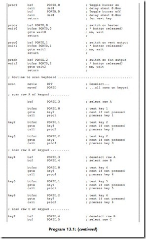
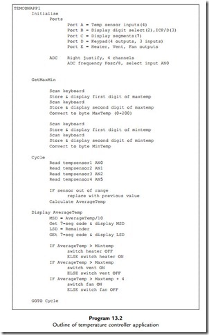
The keyboard scanning routine uses a simple method to check if each key in each row has been pressed, then calls the required action. A more elegant and compact keyboard scanning method is possible when reading in numerical values. A full working program would allow the user to enter the maximum and minimum values for the target temperature, and then go into run mode, where the temperature would be controlled within the set range by operation of the heater, vent and fan. An outline of this application is shown in Program 13.2.


More PIC Applications:Hardware Development

Hardware Development

The circuit was developed using Labcenter™ ISIS schematic capture software, a component of Proteus VSM, which provides animated drawing objects for integrated software and hardware testing (see Appendix E for details). When the circuit had been tested by simulation, a stripboard implementation was devised (Figure 13.4). This layout was designed for an earlier version of the board using the pin-compatible PIC 16F877A chip, with a common anode display, so slight modifications would be needed to implement the TEMCON2 circuit in Figure 13.3.

A demo target system was constructed of this original design, with two filament lamps as the heaters, operating from a high-current 5 V supply. A 5 V central processing unit (CPU) fan was fitted as the cooling element, and the temperature sensors were arranged symmetrically inside the enclosure. The wiring of the target hardware is shown in Figure 13.5. Note that there is a sensor output on the fan that could be used to monitor the actual fan speed, if a suitable interface were added to convert the fan sensor pulse to TTL (transistoretransistor logic) levels. The vent was not physically implemented in this test hardware.

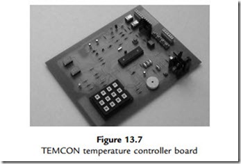
The photograph of the finished system (Figure 13.6) shows the simulator at the right of the picture, with the ICD module (enclosed in ABS box) connected to the ICPD connector on the TEMCON board. Five-volt power supplies and a host PC would complete the system. When final hardware testing was completed, an application board was created using Labcenter ARES™ printed circuit board (PCB) layout software, shown in Figure 13.7. This incorporated an on-board þ5 V supply for operation from a mains adapter.


More PIC Applications:TEMCON2 Temperature Controller

TEMCON2 Temperature Controller

The 16F887 has a comprehensive set of peripheral features, including 14 analogue inputs, three timers, four ECCP (Enhanced Capture Compare PWM) channels, extended universal synchronous asynchronous receiver transmitter (EUSART), MSSP (Master Synchronous Serial Port) and in-circuit debugging (ICD). The ’887 is a pin-compatible replacement for the 16F877A, with some extra features such as additional analogue inputs, comparators and pulse width modulation (PtWM) outputs, an internal oscillator and local interconnect network (LIN) connectivity.

The temperature controller application board TEMCON2 uses most of the available I/O, matching the PIC selected to the application fairly closely. The 8k memory should be sufficient for most application programs that might be developed for this hardware. A demonstration program is provided which will exercise the simulation design and hardware for test purposes.

System Specification

A heating and ventilation system is required to control the environment in a space such as

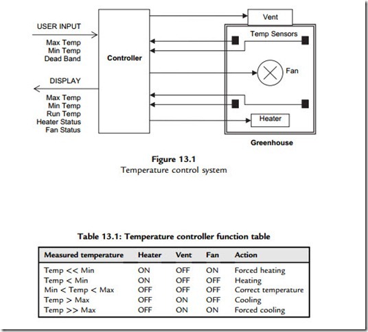
a greenhouse where the temperature must be kept within set limits (0e50oC). A basic block diagram is shown in Figure 13.1.

The unit will be programmed to accept a maximum and minimum temperature, or a set temperature and operating range. The system will operate on the average temperature reading from four sensors, to give a more accurate representation of the overall temperature. Using more than one temperature sensor also allows the system to tolerate a fault in one sensor, if the application firmware includes a check to see if any sensor is out of range. The temperature is maintained by a relay switched heater and vent, and a fan which can be speed controlled via a field effect transistor (FET) output. The fan is fitted to the heater, so that it can be used for forced heating or cooling, depending on whether the heater is on. The FET interface allows speed control of the fan by PWM. The system should operate as specified in Table 13.1.

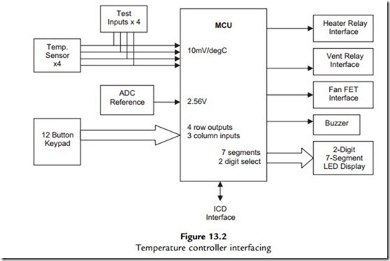
Figure 13.2 shows the interfacing requirements for the application. Four temperature sensors are used to monitor the temperature at different points in the target system. Fortunately, this

PIC Microcontrollers-1315

application does not need much analogue signal conditioning on the input side, other than capacitor decoupling to inhibit noise, and the temperature sensors can be connected directly to the PIC. Their readings can be averaged, or processed with a weighting factor for each, to give a representative value for the measured temperature.

The outputs are controlled via two different interfaces. Relays are used for the heater and vent, assuming that on/off control is suitable. These interfaces are implemented as normally open switched relays, so that an external power supply can be used. The fan output

demonstrates the alternative solid-state interface, using a general purpose power FET. This allows proportional control, but the external circuit must be operated at 5 V. This interface would need to be elaborated for a speed-controlled fan in a full-scale system, and the output could be reallocated to one of the PWM outputs on the 16F887.

PIC Microcontrollers-1316


PIC Motor Applications:Motor Application Board MOT2

Motor Application Board MOT2

We will investigate these ideas via a general purpose motor test board design, MOT2, which can control a dc motor requiring up to 30 A drive current. This is provided by a full bridge driver that allows bidirectional speed and position control with pulse feedback (servo motor). MOT2 is based on the PIC 16F690 (as used in the LPC demo board). A block diagram is shown in Figure 11.2 and a circuit schematic in Figure 11.3.

A variety of motor control operations can be demonstrated using this system:

• Motor On/Off

• Motor Forward/Reverse

• Open/Closed Loop Position Control

• Open/Closed Loop Speed Control.

Command inputs can be received from an 8-bit switch bank, a remote 8-bit master controller, two push buttons, or from the analogue inputs or serial ports. The motor can be turned in either direction via a full bridge driver, providing position and speed control. Pulse width modulation (see Chapter 8) will be used to control the speed. The shaft speed and position are monitored by a shaft encoder, which has three outputs, but only the index output (one pulse per revolution) is connected in the initial design. In the simulation schematic, the motor and encoder are integrated into a single servo motor model, DCM.

PIC Microcontrollers-1285

Motor Drive

A 6 V permanent magnet motor is used since it will run from the same 5 V supply as the PIC. However, a large decoupling capacitor (C4) should be fitted because the motor will generate a lot of noise on the supply, particularly when it switches off. The motor current direction, forward or reverse, is controlled by switching on two of the four MOSFETs from RA4 or RA5. Q1 and Q3 are switched on if RA4 output goes high (motor forward), and Q2 and Q4 if RA5 goes high (motor reverse). Q1 and Q2 switch on when the gate is high (N-FET), but Q3 and Q4 switch on when the gate is low (P-FET), so an inverting bipolar stage is needed on each gate. The current flows diagonally through the bridge and motor to drive it in either direction. The bridge is rated at 30 A, so a range of small to medium dc motors could be driven successfully. In the simulation, the motor characteristics can be adjusted to represent different motors: nominal voltage, coil resistance, coil inductance, zero load rpm, effective mass of the motor and load, and the number of encoder pulses per revolution.

Output Sensor

The rotary encoder represented in the simulation circuit schematic has three outputs. Two have the same number of slots per revolution (adjustable in simulation to represent a range of encoders, default 24), but they are offset by half a slot so that the direction of rotation can be detected from the phase difference in the output signals. The third output generates an index signal once per revolution, which can be used to generate an absolute initial position, or to measure the speed as time per revolution. In hardware, an opto-sensor containing a light- emitting diode (LED) and photodetector can be mounted either side of a perforated wheel attached to the motor shaft. This allows the light to pass through holes or slots causing digital pulses to be output from the sensor via a built-in amplifier, allowing the motor speed or position to be monitored by the controller. The simplest type can have a single slot producing one pulse per revolution. Alternatively, the sensor can work by reflection from a shaft surface, or magnetically. The index output on the simulated servo in Figure 11.3 is connected to the Timer0 (T0CKI) input of the PIC, so that the shaft revolutions can be counted. Alternatively, the pulse interval can be measured using timer mode, if that will produce a more accurate measurement. The pulse may also be used to trigger a Timer0 interrupt.

Switched Inputs

The control program can use the push buttons (S1, S2) connected to RB6 and RB7 to stop, start, or change speed or direction. The binary input switches could be used to select the speed or position. Alternatively, a remotely generated digital control code can be applied to the digital input connector pins (J2) from a master controller, which could be operating a number of motors in a robot system or machine tool. In this case, part of the digital input would be a motor select code, and part would be a position or speed command. Serial commands could also be used, with the port B pins reassigned for this purpose (see Section 12.4). If the parallel input is removed from the circuit, a smaller, cheaper PIC 12FXXX series device could be used instead.

These have six input/output (I/O) pins, so there would be three inputs available with which to control the motor speed, position and/or direction. Analogue inputs are also available, if the motor needs to be voltage controlled.

Analogue Input

The analogue input could be used to receive a voltage that sets the speed or position of the motor. For example, a position servo may use a potentiometer to provide position feedback to the controller, or a temperature sensor might control the speed of a fan. The analogue-to-digital converter (ADC) must be initialized to suit, in this case using the internal supply reference to set the range. For test purposes, a pot is connected to AN10, to provide a dummy analogue input. If the jumper is closed, AN11 can be used to monitor the motor drive current as a voltage across a 0R1 current sensing resistor connected in the common arm of the bridge (100 mV/A). This can be used as a feedback signal or to shut down the output if the motor current is too high. External analogue inputs can be connected at J1.

The default internal clock frequency of the PIC 16F690 is 4 MHz to give an instruction cycle time of 1 ms. The internal clock mode needs to be selected in the configuration word at the top of the program, along with the power-up timer and MCLR enable (00E4h). MCLR is controlled from the programmer during testing, but a reset button is also provided on board. The power-on timer should be enabled during programming to ensure a reliable start. The motor drive will need an external power supply providing sufficient current for the motor connected, so the supply from the programming connector may need to be disconnected at JP2 while programming.


Hardware Prototyping:Dizi84 Applications

Dizi84 Applications

Titles for a set of programs to run on this hardware are suggested below. Three applications (*) will be described in some detail, while a further eight will be specified and the source code listed. These form a set of applications suitable for group assignment work in a training program.

PIC Microcontrollers-1264

PIC Microcontrollers-1265

An ISIS schematic for the DIZI board is shown in Figure 10.12, which allows the above applications to be tested by simulation. All can be downloaded from the support website (www.picmicros.org.uk), and tested in MPLAB if Proteus VSM is not available. If VSM is available, virtual instruments can be used for checking the outputs. The frequency counter and oscilloscope are shown in Figure 10.13.

PIC Microcontrollers-1266

PIC Microcontrollers-1267PIC Microcontrollers-1268

A flowchart for the program BUZZ1 is shown in Figure 10.14. It will generate a single tone at the buzzer when the input button is operated, by toggling the output to the buzzer, with a delay between each change of output state. If a count of 255 is used with a 1 ms instruction cycle time, we have seen that the loop itself will take 255 x 3 x 1 ¼ 765 ms, which will give an output frequency of 106/(765 x 2) ¼ 654 Hz, which is well within the audible range.

This frequency can be adjusted by simply reducing the count value in the delay loop; 654 Hz is the minimum frequency available. A more precise calculation of the delay loop can be used to obtain a more exact frequency, or the hardware timer can be used. In either case, the period can be checked using the stopwatch in the simulator before downloading. The source code is listed in Program 10.1.


Hardware Prototyping:Dizi84 Board Design

Dizi84 Board Design

A circuit will now be designed, and a set of programs provided, to illustrate the hardware design process and programming principles discussed in previous sections. The DIZI board will allow the user to experiment with the various features of the PIC hardware and programming techniques.

Hardware Specification

The microcontroller demonstration board will be suitable for demonstrating a range of processes incorporating display, audio, counting, timing and interrupt operations. The

PIC Microcontrollers-1259

board will have a single-digit seven-segment display for showing output data in hexadecimal or decimal form, and a low-power audio transducer. Manually operated toggle switches will provide a 4-bit parallel input. Two input push buttons will be used for general control (e.g. run, clear), to simulate input events to be counted, or to generate an external interrupt. Timed events should be measured or generated with an accuracy of better than 1%. The circuit will be battery powered, with a push button power switch to ensure that the power cannot be left on, and a power ‘on’ indicator. The board will be as small as possible, and the microcontroller must be easily reprogrammable, with flash memory.

Hardware Implementation

The seven-segment display will require seven outputs from the microcontroller. Active high operation can be provided by a common cathode LED display, and the display decimal point can be used as the power indicator. The audio transducer requires one output. A piezo buzzer has sufficient bandwidth and output power, and its power consumption is low. A miniature DIP switch bank will be used for 4-bit input, and miniature push buttons used, to conserve space.

Fourteen input/output (I/O) pins are required; the PIC 16F84A has only 13, so a chip with more I/O, such as the 16F690, could be considered. However, the audio output and interrupt input can share the same I/O pin, because the high impedance of the buzzer will not interfere with input signals on the same pin. RB0 will be used as the dual function pin, since it is defined as the principal interrupt input, but can also be used as an output. The outputs can source up to 25 mA, but current-limiting resistors will restrict the current per display segment to 10e15 mA to control the maximum load on the port when all the segments are on. The I/O allocation for the project is shown in Table 10.1.

A crystal clock of 4 MHz will be used to obtain the required timing precision, and the convenience of a 1 ms instruction cycle. The 16LF84A-04 (LF ¼ low voltage) can operate from a supply of between 2.0 V and 5.5 V, so the circuit will be powered from 2 x 1.5 V dry cells, giving a 3.0 V supply. The ‘04’ suffix indicates that a maximum 4 MHz clock frequency can be used. A block diagram of the proposed system is shown in Figure 10.8. The inputs and outputs are given the labels that will be assigned in the application programs.

Implementation

A circuit for the DIZI board is shown in Figure 10.9. The PIC 16LF84A drives an active high- (common cathode)elow-current seven-segment LED display at port B, RB1eRB7, via a block of 220R current-limiting resistors. RB0 drives an audio sounder when set as

PIC Microcontrollers-1260

PIC Microcontrollers-1261

an output, but can also be used to detect the ‘Interrupt’ push button when set as an input and the chip is initialized for this option. To prevent RB0 being shorted to ground if set as an output, the spare 220R resistor is connected between the push button and RB0.

This does not affect the operation of the sounder, which has a relatively high resistance. A 4-bit DIP switch input is connected to port A, RA0eRA3, with a push button connected to RA4, which can be used as an external pulse input to the Counter/Timer Register TMR0. These operate as active low inputs with 100k pull-up resistors, as does the interrupt push button.

A stripboard layout for the DIZI board is shown in Figure 10.10. The detail of the component pin connections has been omitted owing to the reduced scale of the illustration, but this information can be obtained from the component pin out data, when selecting particular components. The finished stripboard circuit is shown in Figure 10.11. The

PIC Microcontrollers-1262

PIC Microcontrollers-1263

construction process for a slightly modified board is described in a little more detail in Appendix D.


Program Debugging:Logical Errors

Logical Errors

When all syntax errors have been eliminated the program will assemble successfully, and the hex file will be created. However, this does not necessarily mean that it will function correctly when downloaded to the chip; in fact, it probably won’t! Usually there will be logical errors, particularly when learning the programming method. Mistakes in the program functional sequence or syntax will prevent it operating as required. For instance, the wrong register may be operated on or a loop may execute correctly, but the wrong number of times. There may also be ‘run-time’ errors, that is, mistakes in the program logic that only show up when the program is actually executed. A typical run-time error is ‘Stack Overflow’, which is caused by CALLing a subroutine, but failing to use RETURN at the end of the process. This is not detected by the assembler.

Simulation

Once the program has been successfully assembled, it could be tested by downloading to the hardware and running it. If there are logical errors, and the output is incorrect, the source code must be modified, rebuilt, downloaded and tested again. In the early days of microprocessors this was the only option, but it is time consuming and inefficient. The only way round this was the use of an emulator system, which plugged into the processor socket in place of the MPU and allowed register monitoring, single stepping and breakpoints to be used. Such emulator systems were expensive, and the program read-only memory (ROM) still had to be reprogrammed out of circuit each time the source code was corrected, unless this was also emulated.

Some form of virtual testing of the program sequence was therefore desirable, to eliminate logical errors before downloading. The rise in the use of microcontrollers meant that, in small systems at least, the program memory, processor and peripheral interfaces were all on one chip, which could be simulated in software as a complete package. This allowed the program logic to be tested and modified more quickly, with all the internal registers displayed while tracing through the program for the correct sequence of operations. Source code debugging allows the execution point reached in the source code to be identified while single stepping through the program. Step-over and breakpoint setting allow execution of selected portions of the program at full speed to reach the problem areas or the code quickly.

Thus, a major advantage of the microcontroller over an equivalent discrete microprocessor system is that the design of the chip is fixed, so a full simulation model can be supplied for each device. The Microchip simulator tool MPSIM allows windows to be opened to show the source code, machine code, registers, simulated input, timing checks and so on. The MPLAB development system, including the assembler and simulator, has always been provided free by Microchip to encourage the development of the market for its chips.

Proteus VSM provides an alternative debugging environment, which is integral with ISIS schematic capture. It can be run independently or as a debugging tool from within MPLAB. The latter arrangement is preferred for more complex assembler and C applications, when the MPLAB project management tools are required. For simple assembler programs, MPLAB is not required. The schematic is entered using the ISIS graphics editor, and the program written using the integrated source code editor. It is assembled using the same Microchip MPASM assembler as provided in MPLAB integrated development environment (IDE), which is included in the Proteus package.

The resulting HEX machine code program file is then attached to the MCU. The program can then be run and debugged in a source code window, which includes three single stepping options and simple breakpoints. The procedure for interactive testing in Proteus VSM is detailed in Appendix E.

Program Testing in MPLAB

The simulator must model the operation of the selected microcontroller as completely as possible. The user must be able to provide the inputs that would occur in the actual system, and to monitor the effect on relevant registers, especially the outputs. The program will need to be started and stopped at critical points, single stepped to check the sequence of operations, and timing measured. All possible input events and sequences must be anticipated and tested, to ensure that no unforeseen problems arise when the application is in use.

In MPLAB, with the source code loaded and assembled, select ‘Debugger’, ‘Select Tool’ and ‘MPLAB SIM’ from the main menu. The debugging toolbar should appear with the buttons:

• RUN: Execute the program.

• HALT: Stop the program with the current execution point indicated.

• ANIMATE: Run the program in auto-step mode.

• STEP INTO: Execute program one instruction at a time, including subroutines.

• STEP OVER: Single step current routine, but execute subroutines at full speed.

• STEP OUT: Exit from the current subroutine at full speed and wait.

• RESET: Start again at the top of the program.

These controls allow the source code to be debugged using the single stepping options with breakpoints. Various windows can be opened via the View and Debugger menus, which assist with debugging in MPSIM. The most commonly used are described below (see Figure 9.1).

Edit Window (Open/New File Buttons)

The Edit window is used to create and subsequently modify the source code, PROG1.ASM, as a text file. Ensure it is saved in a project folder with the rest of the assembler fileset, as further simulation files will be added. When the program has been assembled and is then run from the debug controls and halted, the current instruction is indicated in the source code window by a green arrow. Breakpoints can be inserted by double-clicking on the line required, causing a red marker to appear in the margin.

Special Function Register Window (View Menu)

All the special function registers (SFRs) are displayed in this window in hex, binary and decimal (right-click on the column headings bar to select the format). We may want to read

PIC Microcontrollers-1244

The functions of these registers have been described in Chapters 5 and 6. More complex chips have additional SFRs, and the address of a register given here may be different. For example, the 16F887 has ports AeE, using registers 05e09, so the electrically erasable programmable read-only memory (EEPROM) access registers are moved to bank 2, address 10Ch and 10Dh. The SFRs displayed will therefore change according to the chip selected in Configure, Select Device.

Watch Window (View Menu)

A watch window allows selected registers to be displayed, that is, only those of interest in a particular application. SFRs and user-labeled registers are added separately, and the numerical format for each can be selected individually. This allows, for example, counters to be displayed in decimal, and port and status bits in binary.

Simulator Stimulus (Debugger Menu)

In most applications, a sequence of inputs needs to be generated to test the response to all possible combinations. In MPLAB, a workbook is created to specify and store the simulated inputs. The simplest method is to use the Asynch (asynchronous input) table; each input pin is assigned a row in a stimulus table, and is operated manually during the course of the simulation. Alternatively, a schedule of input changes may be created which allow the same test sequence to be generated each time the program is run using the Pin/Register Actions tab.

Stopwatch (Debugger Menu)

The stopwatch window records the simulated time elapsed and number of instructions executed. It can be zeroed to measure intervals between events, for example, the delay created by a software loop, or the period of an output pulse. The MCU clock rate must be entered via the Debugger, Settings dialogue to match the oscillator frequency to be used in hardware.

Trace Window (View Menu)

As the program is executed, the trace window displays a disassembled version of each line with the corresponding machine code and addresses, so the changes can be checked and recorded. At the same time, the original source code is displayed in a lower window.

Logic Analyzer (View Menu)

This displays the input and output bits individually or in groups on a timebase display, as would be seen on an oscilloscope. This gives a much more immediate view of the system performance and allows event timing to be more easily checked.

Setting up MPSIM

The setup for a typical application, MOT1, will now be described step by step. If necessary, assemble the program, using the Project, Quickbuild option, or rebuild the project using the Build All button. Ensure that the correct processor is selected, via the Configure, Select Device dialogue (16F84A for the MOT1 project). At the same time, it is advisable to set the chip fuses via Configure, Configuration Bits. For MOT1, uncheck ‘Configuration Bits set in code’, selecting oscillator ¼ RC, watchdog timer off, power-up timer on and code protection off. Set the processor clock frequency via Debugger, Settings, Osc/Trace (100 kHz for MOT1).

The program can now be run and stopped to make sure the simulator is working. When halted, the current execution point is indicated in the margin of the source code window. We now need to set up the simulator so that the relevant information is displayed and the correct program function can be confirmed, or logical errors corrected. Simply running the program in the simulator does not generally provide enough information to confirm its correct operation, let alone to debug it. Single stepping allows the program to be executed one instruction at time; the registers can then be checked for the right contents as the execution progresses.

In the Watch window, use Add SFR to display the PCL, WREG, PORTA and TRISA registers, and Add Symbol to display the Count and Timer registers using the buttons. Select and right- click on PORTA, select Properties from the drop-down menu and change the display format to binary so the state of the individual bits can be seen. Repeat for TRISA. In the same dialogue, change the format of the Count and Timer registers to decimal.

Testing with Asynchronous Inputs

We are aiming for a setup as shown in Figure 9.1. The simplest method of simulating inputs is the asynchronous stimulus. Single-bit inputs are changed by the user via on-screen buttons while the program is executed in single-step mode. The source code, Stopwatch, Stimulus, Watch and Trace windows are displayed.

The trace facility (View, Simulator Trace) provides a comprehensive record of program execution by displaying the program line from the list file alongside the source and destination register address and contents (SA, SD, DA, DD) after each instruction, as well as the number of cycles completed. This can be saved, printed and studied. The original source code is also displayed in the lower pane when single stepping.

To set up the simulated inputs, select Debugger, Stimulus, New Workbook and the Asynch tab. In the Pin/SFR column, select RA2, RA3 and RA4, and Toggle mode for each in the Action column. Add a comment stating its function. Set all the inputs high by clicking on each fire button and stepping once. Check that the port A input bits are set high in the SFR window.

Reset the program and single step through the initialization sequence. Step through the initialization sequence to the label ‘start’ and check that the register ‘Count’ is initialized correctly. With the ‘run’ input high, the program should wait at the ‘start’ label. Now clear

PIC Microcontrollers-1245

input RA4 by hitting the ‘Fire’ button, and step to the start of the delay sequence. Once in the delay sequence, single stepping is not helpful, so we will now use breakpoints to test the main loop. Set a breakpoint at the ‘cycle’ label by double-clicking in the source code line number margin; a red marker appears. Set a breakpoint at the BCF instruction as well. Reset the program and run to the first breakpoint.

Zero the stopwatch, run to the next breakpoint and note the time (15 ms). Zero the stopwatch again and run to the first breakpoint. The time should be similar (16 ms), indicating a mark/ space ratio (MSR) of approximately 50%. At the same time, check that RA0 is toggling each time, which indicates that the output PWM signal is present.

The up and down control can now be tested. Hit the ‘Up’ button (RA2) and check that the Count value increments for each output cycle. Disable ‘Up’ (high) and enable ‘Down’ (low). The Count value should decrement. Now disable the breakpoints (right-click) and run the program. The Count value should go down to 1 and stop there. Now enable the ‘Up’ input and check that Count goes to its maximum value (255) and stops there. With the breakpoints reinstated, the stopwatch can be used to check the minimum and maximum MSR values.

The single-step facility has two options, ‘step into’ and ‘step over’. Step into means execute all the instructions including those in subroutines. As we have seen above, the delay sequence is not suitable for single stepping as it is repetitive. If the delay is in a subroutine, as in BIN4, step over can be used; this will step through the current routine, but will run any subroutines called at full speed. This allows each program block to be tested separately. However, as the delays in MOT1 are not subroutines, breakpoints are used to allow them to run at full speed.

Testing with Scheduled Inputs

Testing a program can be automated using a stimulus workbook. The state of an input or file register is changed at a particular step in the program, and the same test sequence can then be applied each time the simulation is run, making the testing quicker and easier, particularly in more complex applications.

The workbook is opened via Debugger, Stimulus, New Workbook. Select the ‘Pin/Register Actions’ in the workbook window, and ‘Click here to Add Signals’. The output (RA0) and input (RA2,3,4) bits are added to the active window, and the bit state is changed at specific times, measured in instruction cycles. The stimulus sequence used for MOT1 can be seen in the stimulus window in Figure 9.2.

The simulator logic analyzer in the view menu will provide a time-based trace of changes in individual input/output (I/O) register bits. The Channels button opens a dialogue where the required bits are selected for display. In order to record the outputs over a suitable time period, a break must be set after a suitable number of cycles. This can be setup in the Debugger,

PIC Microcontrollers-1246

Settings dialogue, by checking the Break on Trace Buffer Full box and setting the buffer size to, say, 1000k for the stimulus inputs scheduled in the workbook as above. This provides enough time for the inputs to take effect, over a period of about 10 s.

A trace of the output at RA0 is obtained as shown with these settings (it appears solid at full scale). It can be seen that it is switched on when RA4 (run input) is low, and off when RA4 is high. RA3 (down) low decreases the MSR and RA2 (up) increases it. To see the effect of these inputs on the output waveform, the zoom controls must be used to expand the waveform in a selected area. The overall timescale has to be adjusted so that the duty cycle has enough time to reach the minimum and maximum values. Some experimentation is needed to get the right combination of overall timescale and input timing. The scheduled test allows exactly the same test sequence to be used each time, and a record kept if required, at the cost of increased setup time.