5.1.3 Basic Concepts in Interfacing Output Devices
The concepts in interfacing output devices are similar to those in interfacing memory. The steps can be listed as follows:
1. Decode the low-order address bus to generate a unique pulse corresponding to the port address on the bus; this is called the I/O address (I͞O͞A͞D͞R͞) pulse.
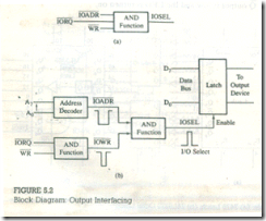
2. Combine (AND) the I/O address pulse (I͞O͞A͞D͞R͞), I͞͞O͞R͞Q͞ , and W͞͞R͞ to generate the IOSEL (I/O select) pulse (Figure 5.2(a)). Another approach is to generate the I͞O͞W͞͞R͞ (I/O Write) by combining I͞͞O͞R͞Q͞ and W͞͞R͞, and then combine I͞O͞W͞͞R͞ with the I͞O͞A͞D͞R͞ (I/O Address) pulse to generate the IOSEL pulse (Figure 5.2(b)). The critical concept here is that the decoded address, I͞͞O͞R͞Q͞, and W͞͞͞R͞ are all necessary to latch the data at the appropriate time; how these signals are combined is often dictated by availability of decoding devices (chips) in the system.
3. Use the IOSEL pulse to enable (activate) the output device.
Let us examine the significance of the I/O select pulse. This pulse is generated by ANDing the decoded address, I͞͞O͞R͞Q͞ , and W͞͞R͞ signals as shown in Figure 5.2(a); all these signals are active low. The assertion of this pulse indicates two pieces of information: (1) the low-order address bus has the port address (07H), and (2) the data byte from the accumulator is on the data bus. Thus, this is the
appropriate time to enable the latch (or open the gate for data). Figure 5.2(b) shows how these control signals are generally ANDed in a typical interfacing circuit to generate the IOSEL pulse and how the I/O select pulse is used to enable the output latch.
