9.9.3 Interfacing with Memories
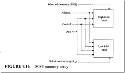
In Figure 9.16, the 16-bit word memory in the 8086 is partitioned into odd and even 8- bit banks on the upper and lower halves of the data bus selected by BHE and A0• This is typically used for RAMs. Note that RAMs are needed when subroutines and interrupts requiring stack are desired in an application.
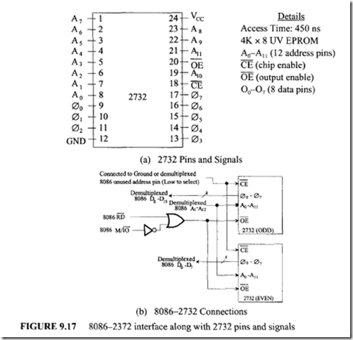
ROMs and EPROMs are the simplest memory chips to interface to the 8086. Because ROMs and EPROMs are read-only devices and the 8086 always reads 16-bit data but discards unwanted bytes (if necessary), A0 and BHE are not required to be part of the chip enable/select decoding (chip enable is similar to chip select decoding except that chip enable also provides whether the chip is in active or standby power mode). The 8086 address lines must be connected to the ROM/EPROM chips starting with A 1 and higher to all the address lines of the ROM/EPROM chips. The 8086 unused address lines can be used as chip enable/select decoding. To interface the ROMs/EPROMs directly to the 8086 multiplexed bus, they must have output enable signals. Figure 9.17 shows the 8086 interfaced to two 2732 chips along with the pin diagram of 2732.
The 8086’s interface to 2732 EPROMs in Figure 9.17(b) does not use 8086 BHE and A0 to distinguish between even and odd 2732s. The 8086 RD and inverted M/10 pins are ORed and connected to the 2732 OE pins. The 8086 CE can be connected to either ground or an unused 8086 address pin. Note that both 2732’s are enabled for all data reads; the odd 2732 places data on the demultiplexed 8086 D8-D15 pins while the even 2732 places data on the demultiplexed 8086 D0-D7 pins. The 8086 reads the desired data and discards unwanted data if necessary depending on byte, odd word address or even word address transfers.
Static RAMs (SRAMs)
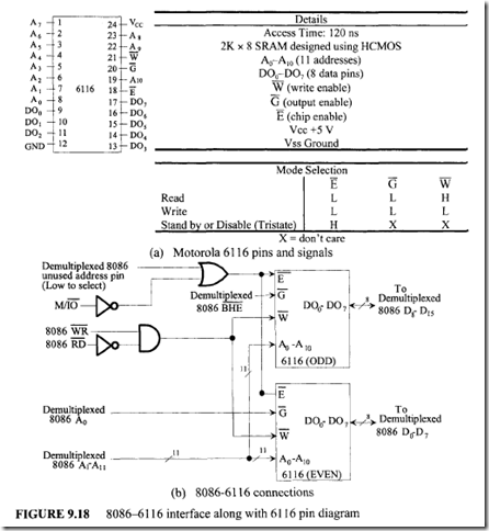
Because static RAMs are read/write memories and data will be written to RAM(s) once selected by the 8086, both A0 and BHE must be included in the chip select logic. For each static RAM, the data lines must be connected to either the upper half (AD15-AD8) or the lower half (AD7-AD0) of the 8086 data lines. Figure 9.18 shows the 8086 interface to two 6116 static RAMs along with the pin diagram of the 6116. Note that the 6116 signals, W (Write Enable), G (Output enable), and E (Chip enable) are decoded as follows: when G = 0 and E = 0, then W = I for read and W = 0 for write.
In Figure 9.18, the 8086 demultiplexed BHE signal is used to select odd 6116 SRAM chips; the data lines of this odd 6116 are connected to the demultiplexed 8086 D8-D15 pins. The 8086 demultiplexed A0 signal, on the other hand, is used to select even 6116 SRAM chip; the data lines of this even 6116 are connected to the demultiplexed 8086
D0-D7 pins. Note that the 6116 has two chip enables E and G along with a single read/write pin (W) .When the 6116 is enabled, W = 1 for read and G = 0 for write.
Dynamic RAMs (DRAMs)
![]() Dynamic RAMs store information as charges in capacitors. Because capacitors can hold charges for a few milliseconds, refresh circuitry is necessary in dynamic RAMs for retaining these charges. Therefore, dynamic RAMs are complex devices to use to design a system. To relieve the designer of most of these complicated interfacing tasks, Intel provides dynamic RAM controllers to interface with the 8086 to build a dynamic memory system. Dynamic RAMs are used for microcomputers requiring large memories. DRAMs are typically used when memory requirements are 16k words or larger. DRAM is addressed via row and column addressing. For example, one megabit DRAM requiring 20 address bits is addressed using 10 address lines and two control lines, RAS (Row Address Strobe) and CAS (Column Address Strobe). To provide a 20-bit address into the DRAM, a LOW is applied to RAS and 10 bits of the address are latched. The other 10 bits of the address are applied next and CAS is then held LOW.
Dynamic RAMs store information as charges in capacitors. Because capacitors can hold charges for a few milliseconds, refresh circuitry is necessary in dynamic RAMs for retaining these charges. Therefore, dynamic RAMs are complex devices to use to design a system. To relieve the designer of most of these complicated interfacing tasks, Intel provides dynamic RAM controllers to interface with the 8086 to build a dynamic memory system. Dynamic RAMs are used for microcomputers requiring large memories. DRAMs are typically used when memory requirements are 16k words or larger. DRAM is addressed via row and column addressing. For example, one megabit DRAM requiring 20 address bits is addressed using 10 address lines and two control lines, RAS (Row Address Strobe) and CAS (Column Address Strobe). To provide a 20-bit address into the DRAM, a LOW is applied to RAS and 10 bits of the address are latched. The other 10 bits of the address are applied next and CAS is then held LOW.
The addressing capability of the DRAM can be increased by a factor of 4 by adding one more bit to the address line. This is because one additional address bit results into one additional row bit and one additional column bit. This is why DRAMs can be expanded to larger memory very rapidly with inclusion of additional address bits. External logic is required to generate the RAS and CAS signals, and to output the current address bits to the DRAM.
DRAM controller chips take care of refreshing and timing requirements needed by the DRAMs. DRAMs typically require 4 millisecond refresh time. The DRAM controller performs its task independent of the microprocessor. The DRAM controller sends a wait signal to the microprocessor if the microprocessor tries to access memory during a refresh cycle.
Because oflarge memory, the address lines should be buffered using 74LS244 or 74HC244 (Unidirectional buffer), and data lines should be buffered using 74LS245 or 74HC245 (Bidirectional buffer) to increase the drive capability. Also, typical multiplexers such as 74LS157 or 74HC157 can be used to multiplex the microprocessors address lines into separate row and column addresses.


