7.1 Chip Organization
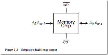
A simplified pinout of a RAM chip is shown in Figure 7-3. An m-bit address,
having lines numbered from 0 to m-1 is applied to pins A0-Am-1, while asserting CS (Chip Select), and either WR (for writing data to the chip) or WR (for reading data from the chip). The over bars on CS and WR indicate that the chip is selected when CS=0 and that a write operation will occur when WR=0. When reading data from the chip, after a time period tAA (the time delay from when the address lines are made valid to the time the data is available at the output), the w-bit data word appears on the data lines D0– Dw-1. When writing data to a chip, the data lines must also be held valid for a time period tAA. Notice that the data lines are bidirectional in Figure 7-3, which is normally the case.
The address lines A0- Am-1 in the RAM chip shown in Figure 7-3 contain an address, which is decoded from an m-bit address into one of 2m locations within the chip, each of which has a w-bit word associated with it. The chip thus contains 2m´w bits.
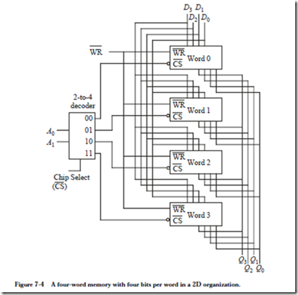
Now consider the problem of creating a RAM that stores four four-bit words. A RAM can be thought of as a collection of registers. We can use four-bit registers to store the words, and then introduce an addressing mechanism that allows one of the words to be selected for reading or for writing. Figure 7-4 shows a design
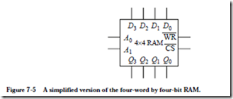
for the memory. Two address lines A0 and A1 select a word for reading or writing via the 2-to-4 decoder. The outputs of the registers can be safely tied together without risking an electrical short because the 2-to-4 decoder ensures that at most one register is enabled at a time, and the disabled registers are electrically disconnected through the use of tri-state buffers. The Chip Select line in the decoder is not necessary, but will be used later in constructing larger RAMs. A simplified drawing of the RAM is shown in Figure 7-5 .
There are two common ways to organize the generalized RAM shown in Figure 7-3. In the smallest RAM chips it is practical to use a single decoder to select one
out of 2m words, each of which is w bits wide. However, this organization is not economical in ordinary RAM chips. Consider that a 64M´1 chip has 26 address lines (64M = 226). This means that a conventional decoder would need 226 26-input AND gates, which manifests itself as a large cost in terms of chip area – and this is just for the decode.
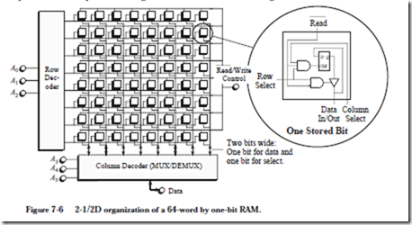
Since most ICs are roughly square, an alternate decoding structure that significantly reduces the decoder complexity decodes the rows separately from the columns. This is referred to as a 2-1/2D organization. The 2-1/2D organization is by far the most prevalent organization for RAM ICs. Figure 7-6 shows a 26-word
x1-bit RAM with a 2 1/2D organization. The six address lines are evenly split between a row decoder and a column decoder (the column decoder is actually a MUX/DEMUX combination). A single bidirectional data line is used for input and output.
During a read operation, an entire row is selected and fed into the column MUX, which selects a single bit for output. During a write operation, the single bit to be written is distributed by the DEMUX to the target column, while the row decoder selects the proper row to be written.
In practice, to reduce pin count, there are generally only m/2 address pins on the chip, and the row and column addresses are time-multiplexed on these m/2 address lines. First, the m/2-bit row address is applied along with a row address strobe, RAS, signal. The row address is latched and decoded by the chip. Then the m/2-bit column address is applied, along with a column address strobe, CAS. There may be additional pins to control the chip refresh and other memory functions.
Even with this 2-1/2D organization and splitting the address into row and col- umn components, there is still a great fanin/fanout demand on the decoder logic gates, and the (still) large number of address pins forces memory chips into large footprints on printed circuit boards (PCBs). In order to reduce the fanin/fanout constraints, tree decoders may be used, which are discussed in Section 7.8.1. A newer memory architecture that serializes the address lines onto a single input pin is discussed in Section 7.9.
Although DRAMs are very economical, SRAMs offer greater speed. The refresh cycles, error detection circuitry, and the low operating powers of DRAMs create a speed difference that is roughly 1/4 of SRAM speed, but SRAMs also incur a significant cost.
The performance of both types of memory (SRAM and DRAM) can be improved. Normally a number of words constituting a block will be accessed in succession. In this situation, memory accesses can be interleaved so that while one memory is accessing address Am, other memories are accessing Am+1, Am+2, Am+3 etc. In this way the access time for each word can appear to be many times faster.
7.3.1 CONSTRUCTING LARGE RAMS FROM SMALL RAMS
We can construct larger RAM modules from smaller RAM modules. Both the word size and the number of words per module can be increased. For example, eight 16M ´ 1-bit RAM modules can be combined to make a 16M ´ 8-bit RAM module, and 32 16M ´ 1-bit RAM modules can be combined to make a 64M ´ 8-bit RAM module.
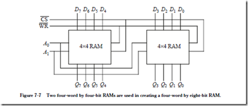
As a simple example, consider using the 4 word ´ 4-bit RAM chip shown in Figure 7-5, as a building block to first make a 4-word ´ 8-bit module, and then an 8-word ´ 4-bit module. We would like to increase the width of the four-bit words and also increase the number of words. Consider first the problem of increasing the word width from four bits to eight. We can accomplish this by simply using two chips, tying their CS (chip select) lines together so they are both selected together, and juxtaposing their data lines, as shown in Figure 7-7.
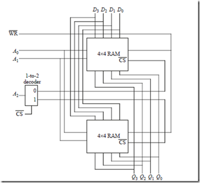
Consider now the problem of increasing the number of words from four to eight. Figure 7-8 shows a configuration that accomplishes this. The eight words are distributed over the two four-word RAMs. Address line A2 is needed because there are now eight words to be addressed. A decoder for A2 enables either the upper or lower memory module by using the CS lines, and then the remaining address lines (A0 and A1) are decoded within the enabled module. A combination of these two approaches can be used to scale both the word size and number of words to arbitrary sizes.
7.4 Commercial Memory Modules
Commercially available memory chips are commonly organized into standard configurations. Figure 7-9 (Texas Instruments, 1991) shows an organization of eight 220-bit chips on a single-in-line memory module (SIMM) that form a 220 ´ 8 (1MB) module. The electrical contacts (numbered 1 – 30) all lie in a single line. For 220 memory locations we need 20 address lines, but only 10 address lines (A0 – A9) are provided. The 10-bit addresses for the row and column are loaded separately, and the Column Address Strobe and Row Address Strobe signals are applied after the corresponding portion of the address is made available. Although this organization appears to double the time it takes to access any par-
ticular memory location, on average, the access time is much better since only the row or column address needs to be updated.
The eight data bits on lines DQ1 – DQ8 form a byte that is read or written in parallel. In order to form a 32-bit word, four SIMM modules are needed. As with the other “active low” signals, the Write Enable line has a bar over the corresponding symbol ( W ) which means that a write takes place when a 0 is placed on this line. A read takes place otherwise. The RAS line also causes a refresh operation, which must be performed at least every 8 ms to restore the charges on the capacitors.
