THE PENTIUM II, PENTIUM III, PENTIUM 4, AND CORE2 MICROPROCESSORS
INTRODUCTION
The Pentium II, Pentium III, Pentium 4, and Core2 microprocessors may well signal the end to the evolution of the 32-bit architecture with the advent of the Itanium1 and Itanium II micro- processors from Intel. The Itanium is a 64-bit architecture microprocessor. The Pentium II, Pentium III, Pentium 4, and Core2 architectures are extensions of the Pentium Pro architecture, with some differences. The most notable difference is that the internal cache from the Pentium Pro architecture has been moved out of the microprocessor in the Pentium II. Another major change is that the Pentium II is not available in integrated circuit form. Instead, the Pentium II is found on a small plug-in circuit board called a cartridge along with a separate level 2 cache chip. Various versions of the Pentium II are available. The Celeron2 is a version of the Pentium II that does not contain the level 2 cache on the Pentium II circuit board. The Xeon3 is an enhanced version of the Pentium II that contains up to a 2M-byte cache on the circuit board.
Similar to the Pentium II, early Pentium III microprocessors were packaged in a cartridge instead of an integrated circuit. More recent versions, such as the Coppermine, are again pack- aged in an integrated circuit (370 pins). The Pentium III Coppermine, like the Pentium Pro, contains an internal cache. The Pentium 4 is packaged in a larger integrated circuit, with 423 or 478 pins and most recently the Pentium 4 and Core 2 are manufactured in a 775-pin LGA pack- age (leadless grid array). The Pentium 4 also uses physically smaller transistors, which makes it much smaller and faster than the Pentium III. To date Intel has released versions of the Pentium 4 and Core2 that operate at frequencies over 3 GHz with a limit of possibly 10 GHz at some future date. Also available to the Pentium 4 and Core2 are the extreme model with a 2M-byte cache and the extreme edition model with a 4M-byte cache. These versions are available in the 65 nm (0.065 micron) form as compared to earlier P4 microprocessors that use the 0.13 micron form. The latest versions are the Core2 Duo and Core2 Quad versions that use 45 nm technology and either two or four cores.
CHAPTER OBJECTIVES
Upon completion of this chapter, you will be able to:
1. Detail the differences between the Pentium II, Pentium III, Pentium 4, and Core2 and prior Intel microprocessors.
1Itanium is a registered trademark of Intel Corporation. 2Celeron is a registered trademark of Intel Corporation. 3Xeon is a registered trademark of Intel Corporation.
2. Explain how the architectures of the Pentium II, Pentium III, Pentium 4, and Core2 improve system speed.
3. Explain how the basic architecture of the computer system has changed by using the Pentium II, Pentium III, Pentium 4, and Core2 microprocessors.
4. Detail the changes to the CPUID instruction and model-specific registers.
5. Describe the operation of the SYSENTER and SYSEXIT instructions.
6. Describe the operation of the FXSAVE and FXRSTOR instructions.
INTRODUCTION TO THE PENTIUM II MICROPROCESSOR
Before the Pentium II or any other microprocessor can be used in a system, the function of each pin must be understood. This section of the chapter details the operation of each pin, along with the external memory system and I/O structures of the Pentium II microprocessor.
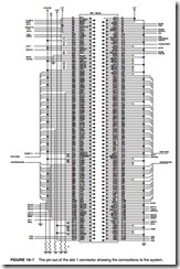
Figure 19–1 illustrates the basic outline of the Pentium II microprocessor slot 1 connector and the signals used to interface to the chip set. Figure 19–2 shows a simplified diagram of the components on the cartridge, and the placement of the Pentium II cartridge and bus components in the typical Pentium II system. There are 242 pins on the slot 1 connector for the microprocessor. (These connections are a reduction in the number of pins found on the Pentium and the Pentium II microprocessors.) The Pentium II is packaged on a printed circuit board instead of the integrated circuits of the past Intel microprocessors. The level 1 cache is 32K bytes as it was in the Pentium Pro, but the level 2 cache is no longer inside the integrated circuit. Intel changed the architecture so that a level 2 cache could be placed very close to the microprocessor. This change makes the microprocessor less expensive and still allows the level 2 cache to operate eficiently. The Pentium level 2 cache operates at one half the microprocessor clock frequency, instead of the 66 MHz of the Pentium microprocessor. A 400 MHz Pentium II has a cache speed of 200 MHz. The Pentium II is available in three versions. The first is the full-blown Pentium II, which is the Pentium II for the slot 1 connector. The second is the Celeron, which is like the Pentium II, except that the slot 1 circuit board does not contain a level 2 cache; the level 2 cache in the Celeron system is located on the main board and operates at 66 MHz. The most recent version is the Xeon, which, because it uses a level 2 cache of 512K, 1M, or 2M, represents a significant speed improvement over the Pentium II. The Xeon’s level 2 cache operates at the clock frequency of the microprocessor. A 400 MHz Xeon has a level 2 cache speed of 400 MHz, which is twice the speed of the regular Pentium II.
The early versions of the Pentium II require a 5.0 V, 3.3 V, and variable voltage power sup- ply for operation. The main variable power supply voltages vary from 3.5 V to as low as 1.8 V at the microprocessor. This is known as the core microprocessor voltage. The power-supply current averages 14.2 A to 8.4 A, depending on the operating frequency and voltage of the Pentium II. Because these currents are significant, so is the power dissipation of these microprocessors. At present, a good heat sink with considerable airflow is required to keep the Pentium II cool. Luckily, the heat sink and fan are built into the Pentium II cartridge. The latest versions of the Pentium II have been improved to reduce the power dissipation.
Each Pentium II cartridge output pin is capable of providing at least 36 mA of current at a logic 0 level on the signal connections. Some of the output control signals provide only 14 mA of current. Another change to the Pentium II is that the outputs are open-drain and require an external pull-up resister for proper operation.
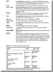
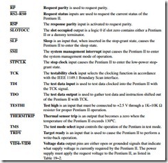
The function of each Pentium II group of pins follows:
A20 Address A20 mask is an input that is asserted in the real mode to signal the Pentium II to perform address wraparound, as in the 8086 microprocessor, for use of the HIMEM.SYS driver.
The Memory System
The memory system for the Pentium II microprocessor is 64G bytes in size, just like the Pentium Pro microprocessor. Both microprocessors address a memory system that is 64 bits wide with an address bus that is 36 bits wide. Most systems use SDRAM operating at 66 MHz or 100 MHz for the Pentium II. The SDRAM for the 66 MHz system has an access time of 10 ns and the SDRAM for the 100 MHz system has an access time of 8 ns. The memory system, which connects to the chip set, is not illustrated in this chapter. Refer to earlier chapters to see the organization of a 64-bit-wide memory system without ECC.
The Pentium II memory system is divided into eight or nine banks that each store a byte of data. If the ninth byte is present, it stores an error-checking code (ECC). The Pentium II, like the 80486–Pentium Pro, employs internal parity generation and checking logic for the memory system’s data bus information. (Note that most Pentium II systems do not use parity checks, but it is available.) If parity checks are employed, each memory bank contains a ninth bit. The 64-bit- wide memory is important to double-precision floating-point data. Recall that a double-precision floating-point number is 64 bits wide. As with the Pentium Pro, the memory system is numbered in bytes from byte 000000000H to byte FFFFFFFFFH. Please note that none of the current chip sets support more than 1G byte of system memory, so the additional address connections are for
The Memory System
The memory system for the Pentium II microprocessor is 64G bytes in size, just like the Pentium Pro microprocessor. Both microprocessors address a memory system that is 64 bits wide with anaddress bus that is 36 bits wide. Most systems use SDRAM operating at 66 MHz or 100 MHz
for the Pentium II. The SDRAM for the 66 MHz system has an access time of 10 ns and the SDRAM for the 100 MHz system has an access time of 8 ns. The memory system, which connects to the chip set, is not illustrated in this chapter. Refer to earlier chapters to see the organization of a 64-bit-wide memory system without ECC.
The Pentium II memory system is divided into eight or nine banks that each store a byte of data. If the ninth byte is present, it stores an error-checking code (ECC). The Pentium II, like the 80486–Pentium Pro, employs internal parity generation and checking logic for the memory system’s data bus information. (Note that most Pentium II systems do not use parity checks, but it is available.) If parity checks are employed, each memory bank contains a ninth bit. The 64-bitwide memory is important to double-precision floating-point data. Recall that a double-precision floating-point number is 64 bits wide. As with the Pentium Pro, the memory system is numbered in bytes from byte 000000000H to byte FFFFFFFFFH. Please note that none of the current chip sets support more than 1G byte of system memory, so the additional address connections are for
future expansion. Figure 19–3 illustrates the basic memory map of the Pentium II system, using the AGP for the video card.
The memory map for the Pentium II system is similar to the map illustrated in earlier chapters, except that an area of the memory is used for the AGP area. The AGP area allows the video card and Windows to access the video information in a linear address space. This is unlike the 128K-byte window in the DOS area for a standard VGA video card. The benefit is much faster video updates because the video card does not need to page through the 128K-byte DOS video memory.
Transfers between the Pentium II and the memory system are controlled by the 440 LX or 440 BX chip set. Data transfers between the Pentium II and the chip set are eight bytes wide. The chip set communicates to the microprocessor through the five REQ signals, as listed in Table 19–3. In essence, the chip set controls the Pentium II, which is a departure from the traditional method of connecting a microprocessor to the system directly to the memory.
The Pentium II connects only directly to the cache, which is on the Pentium II cartridge. As mentioned, the Pentium II cache operates at one half the clock frequency of the micro- processor. Therefore, a 400 MHz Pentium II cache operates at 200 MHz. The Pentium II Xeon
Input/Output System
The input/output system of the Pentium II is completely compatible with earlier Intel micro- processors. The I/O port number appears on address lines A15–A3 with the bank-enable signals used to select the actual memory banks used for the I/O transfer. Transfers are controlled by the chip set, which is a departure from the standard microprocessor architecture before the Pentium II.
Beginning with the 80386 microprocessor, I/O privilege information is added to the TSS segment when the Pentium II is operated in the protected mode. Recall that this allows I/O ports to be selectively inhibited. If the blocked I/O location is accessed, the Pentium II generates a type 13 interrupt to signal an I/O privilege violation.
System Timing
As with any microprocessor, the system timing signals must be understood in order to interface the microprocessor, or so it was at one time. Because the Pentium II is designed to be controlled by the chip set, the timing signals between the microprocessor and the chip set have become proprietary to Intel.


