BJT DRIVER
Context
● You are developing an embedded application using one or more members of the 8051 family of microcontrollers.
● You are designing an appropriate hardware foundation for your application.
Problem
How do you drive DC loads requiring currents of up to around 2A, from the port of an 8051 microcontroller?
Background
A bipolar-junction transistor (BJT) is a three-terminal semiconductor device, devel- oped in the early 1950s. The full name (or acronym) will be used here to distinguish this pattern from the FET (field-effect transistor) considered later in this chapter.
As far as we are concerned, a BJT is most useful as a current-controlled switch. We will not be concerned here with details of their underlying operation but will, instead, focus on the ways in which these transistors may be used to allow a micro- controller to drive a medium-power DC load.
Solution
BJT transistors come in two basic forms: PNP and NPN (Figure 7.15).
[Note: For our purposes, the main value of the BJT is that it acts as a voltage controlled switch. In the case the PNP device, current flow- ing from the base is used to control a much larger current through the load. In the case of the NPN device, current flowing into the base of the device performs the same function.]
To ‘turn on’ the transistor, we need to supply (in the case of NPN) or sink (in the case of PNP) a base current given by the formula:
where hfe is the transistor ‘gain’. This varies from values of around 15 to around 800: values of 100 are typical for the types of devices we are considering. As previously noted, the pins of an 8051 device can sink or source around 20 mA of current (at most): thus, using a suitable BJT, we can control currents of up to around 2A (20 mA multipled by hfe).
We will give two specific examples here: a PNP transistor switch and an NPN transistor switch.
A PNP transistor switch
To illustrate the type of BJT application we will be concerned with in this pattern, consider Figure 7.16. This shows a small lamp (5V, 500 mA), connected to a PNP tran- sistor. Note that, in this circuit, almost any PNP transistor will work, provided it has an hfe value of around 100 (given on the data sheet), and can handle a collector cur- rent of around 500 mA. Note that in this case, a Zetex ZTX 751 transistor is used. This can control a (collector) current of up to 2A, which is a suitable level for a wide range of applications. Such devices are not expensive: expect to pay around $0.30 per tran- sistor (multiples of 1,000 devices).
Briefly, the circuit operates as follows. When the microcontroller pin is at Logic 0, current will flow out of the base of the transistor, driving the device into saturation: the required load current will then flow and the lamp will light. When the microcon- troller pin is at Logic 1, however, no current will flow from the base of the transistor and the load current will be (essentially) 0.
Overall, the significant thing about this circuit is that a very small control current flow- ing out of the base of the transistor (Ibase in the figure) controls the flow of a much larger current (Iload) flowing through the lamp. This is the basis of all BJT interface circuits.
Pull-up resistors
When using this pattern, you may need to incorporate pull-up resistors in your hard- ware design. (See NAKED LED [page 110].)
Buffering the output
We use BJTs to allow us to control comparatively high-power loads. The loads can change: for example, devices can short-circuit, motors can stall or the whole device may suffer physical damage. In such circumstances, the microcontroller port can be subject to high voltages and / or currents. This may result in the whole microcon- troller being rendered inoperative.
[Note: See NAKED LED [page 110] for details of pull-up resistors, one of which may be required here. Note the lamp supply voltage is, here, assumed to be 5V: however, the load supply voltage need not be the same as the controller supply voltage.]
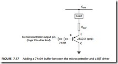
In many circumstances, it is safer to use a buffer to protect the microcontroller in the event of a problem with the load or BJT driver. Figure 7.17 shows a suitable circuit.
Note that we have used two inverter gates to obtain the required logic. As multiple gates are available on a single 74×04, and this is a low-cost buffer, this can be a good solution. Alternatively, the 74×241-based circuit in Figure 7.18 may be used.
Note that, for reasons discussed in IC BUFFER [page 118], a pull-up resistor may be required at the base of the transistor in both of these buffer circuits, if you use TTL technology.
In Figure 7.19 we have used an inverter to both invert the port output (so that a Logic 0 output is now required to drive the load) and to provide a degree of isolation between the transistor and the microcontroller.
Note that in Figure 7.19, we need to ‘source’ current: that is, the direction of conven- tional current flow is into the base of the transistor. As we discussed in NAKED LOAD [page 115], the need to source current may be problematic in some circumstances. For this reason, drivers based on PNP transistors can be slightly more portable.
Hardware resource implications
Every implementation of this pattern uses at least one port pin.
Reliability and safety implications
Pin reset values
After the system is reset, the contents of the various port special function registers (SFRs) are set to 0xFF. This fact has very important safety and reliability implications.
Consider, for example, that you have connected a motorized device to a port and that the device is activated by a ‘Logic 1’ output: that is, a ‘1’ output on a port pin. When the microcontroller is reset, the motorized device may be activated and begin moving. Even if you set the port outputs to 0 at the start of your program, the motor may be ‘pulsed’ briefly, before you are able to stop it. This can, in some systems, lead to the injury or even death of users of the system or those in the immediate vicinity of the system.
Because the output pins are ‘reset high’ it is important to ensure that any devices which have safety implications are connected to the microcontroller in such a way that they are ‘active low’: that is, that an output of ‘0’ on the relevant port pin will activate the device.
Switching on lamps and DC motors
We have presented various equations in this chapter that allow the value of series resis- tors to be calculated for use in drive circuits like that shown in Figure 7.19. In presenting such equations we have implicitly assumed that the load resistance itself is fixed.
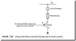
In fact, not all devices present a fixed resistive load. For example, when controlling lamps or DC motors, the initial current required may be very high. This surge of cur- rent may last several hundreds of milliseconds, before it settles to the steady-state value. Your drive circuit needs to be capable of surviving the initial current surge.
One way of dealing with inrush currents is to ‘over rate’ your drive circuit. This means that if, for example, your load is a lamp or motor with a steady-state current requirement of (say) 1A, you should rate your drive circuit at (say) 10A or more, so that you can deal with the inrush current. Please note that it is seldom possible to guess the likely inrush currents. Check the data sheets – they will provide this infor- mation. In the absence of accurate data, assume a factor of at least 10.
Another way of solving this problem is to use what is known as a thermistor in series with the load (Figure 7.20). These have a resistance of around 1–2 Ω when cold: when they warm up (which they do when carrying current) the resistance drops around 0 Ω. Even a small amount of initial resistance will greatly reduce the impact of the inrush current.
Please also note that it is easy to overlook or ignore this issue. Not all drive cir- cuits will fail immediately if subjected to excessive loads and your test circuit may operate reliably on the bench. However, stressing any drive circuit beyond its maxi- mum ratings will dramatically shorten its useful life and it will fail in the field. If in any doubt: over rate by at least a factor of 10 and add a thermistor.
Switching off inductive DC loads
Just because you have managed to switch on a load safely does not, unfortunately, mean that you problems are solved, if your load is inductive.
An inductive load is anything containing a coil of wire: common examples are electromechanical relays and motors. Switching off such loads must be carried out with great caution because, when the current is removed, the voltage across the inductor will increase rapidly. The rapid increase in voltage occurs because the opera- tion of the inductor is defined by the equation:
Here, V is the voltage across the inductor, L is the inductance, and dI/dt is the rate of change of current flow. If we suddenly remove the current (that is, ‘switch off’ the inductor), the resulting rapid change in current will be translated into a rapid voltage increase. This ‘inductive kick’ can be enough to destroy logic gates or any other form of drive circuitry linked to the load. To protect these circuits, a diode can be used to block the ‘kick’ (Figure 7.21).
Please note that the diode used must be able to handle not only the steady-state current but also the turn-off current. The ubiquitous and cheap 1N4004 diode can handle 1A, and is appropriate for many circuits. Where this is not sufficient, a wide range of other capacities are available: for example, the 1N5401 (3A, 100V), the 40HF10 (40A, 100V) or the 70UR60 (250A, 600V). Note that the prices increase dra- matically with current capacity: the low-power diodes cost a few cents, while the high-power alternatives may cost $10.00.
Please note (again) that it is easy to overlook or ignore this issue. Not all drive circuits will fail immediately if subjected to excessive loads and your test circuit may operate reliably on the bench. However, stressing any drive circuit beyond its maxi- mum ratings will dramatically shorten its useful life and it will fail in the field. If in any doubt, use a suitable diode or resistor.
Protecting again load faults
The use of thermistors, diodes and inrush resistors is designed to protect the switch- ing circuit under normal conditions. When working with high-power loads, you also need to deal with the problems caused by damage to the load. In particular, we need to consider the possibility that the load will be short-circuited.
A particular problem arises with semiconductor switching devices such as BJTs. The thermal mass of such semiconductor devices is very low: this means that an excessive current flow – caused, for example, by a short or a stalled motor – will very rapidly take the device out of the safe operating region (see Lander, 1993; or Rashid, 1993, for details). To protect against this, it is essential that you use a fuse in series with the load.
Note that an ‘ordinary’ fuse will not be adequate: the fuse must blow very rapidly to avoid damage to the semiconductor device: such devices are usually labelled ‘high speed’ and will be described as being suitable for semiconductor protection.
Portability
These techniques work with all 8051s (and most other microcontroller and micro- processor families).
As usual, if working with port pins that do not have internal pull-up resistors, you need to include such resistors (10K will do) in your design.
Overall strengths and weaknesses
Software developers sometimes seem to hold the view that discrete transis- tors are ‘old fashioned’ and have now been replaced by IC equivalents. This is not the case. In many applications, particularly where a small number of relatively low- and medium-power drivers are required, discrete transistors are widely used, not least because they are available for under $0.10 each (around half the price of ICs), even in small quantities: as such they can rep- resent a very cost-effective solution.
BJTs can operate at very low voltages, compatible with low-voltage micro- controllers.
The maximum BJT gain of around 100 means that, in most circumstances, we are restricted to current flows of around 1A–2A, if we use a single transistor. Single MOSFETs, by comparison, can readily switch loads of 100A.
The switching speed of transistors (and in particular the switch-off speed) can be around 0.5 µs. This may sound fast, but, particularly in some pulse-width modu- lation applications (see HARDW ARE PWM [page 742]), may not be fast enough.
Related patterns and alternative solutions
The main alternatives to the BJT DRIVER are IC DRIVER [page 134] and MOSFET DRIVER
Example: Driving a high-power IR LED transmitter
Infra-red (IR) LEDs are widely used in domestic applications for remote control. They are also a component in many security systems. IR LEDs often have higher current requirements than conventional LEDs, but are otherwise connected in the same way.
For example, the Siemens SFH485 IR LED requires a current of 100 mA, at a for- ward voltage of 1.5V. If we wish to drive this LED using (say) Port 1 of an 8051 microcontroller, then a variation on the circuit from Figure 7.16 can be used.
Here, we will use a low-cost (PNP) transistor: a 2N2905. This can handle a maxi- mum load current of 600 mA. With ILED at 100 mA, a supply voltage of 5V and an
LED forward voltage of 1.5V, the required value of R2 is:
The saturation voltage (VCE) for the transistor of 0.4V is taken from the transistor data sheet.
Here we would use the next standard resistor value, in this case 33Ω. Note that the nearest value is 30Ω: however, by using this we run the slight risk of running the LED at too high a forward voltage, and reducing the life of this component.


