Microcontroller Architecture
The architecture (internal hardware arrangement) of a complex chip is best represented as a block diagram. This allows the overall operation to be described without having to analyze the internal circuit, which is extremely complex, in detail. PIC data sheets contain a definitive block diagram for each chip. Our starting point is the PIC 16F84A chip, because it has all the basic features but none of the more advanced elements that will be covered later. Also, the model for this chip is provided in the entry-level Proteus VSM microcontroller simulation package. Unfortunately, this chip is now effectively obsolete for new designs and is relatively expensive compared with more recently introduced chips, which actually have more features, such as the 16F690 that we will examine later on.
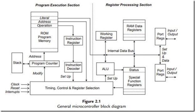
Simplified versions of the block diagrams from the data sheets will be used to help explain particular aspects of the chip operation. A general block diagram that shows some of the common features of PIC microcontrollers is seen in Figure 2.1. It shows that the MCU can be considered in two parts: the program execution section and the register processing section. Note that the program and data are accessed separately, and do not share the same data bus, as is the case within some processor systems. This arrangement, known as Harvard architecture, increases overall program execution speed. The timing and control block coordinates the operation of the two parts as determined by the program instructions, and responds to external control inputs, such as the reset and interrupts.
The program execution section contains the program memory, instruction register and control logic, which store, decode and execute the program. The register processing section has a block of random access memory (RAM), which starts with the special function registers (SFRs) that are used to control the processor operations, including the port registers, which are used for input and output. The rest of this RAM block provides general purpose registers (GPRs) for
data storage. The arithmetic and logic unit (ALU) processes the data, e.g. add, subtract and compare.
In some microcontrollers and microprocessors, the main data register is called the accumulator (A), but the name working register (W), used in the PIC system, is a better description. It holds the data that the processor is working on at the current time, and most data has to pass through it. For example, if a data byte is to be transferred from the port register to a RAM data register, it must be moved into W first. The working register works closely with the ALU in the data processing operations. Instructions may operate on W or on the RAM register, which includes the ports and SFRs.
