Programmable Interval Timer 8253
1. Draw the pin diagram of 8253.
Ans. The pin diagram of 8253 is shown below:
2. Draw the functional block diagram of 8253.
Ans. The functional block diagram of 8253 is shown below:
The figure shows that there are six blocks interconnected by an internal data bus. The six blocks include three counters (counter 0, 1 and 2), a data bus buffer, a Read/Write logic and a control word register.
3. How many counters are there in 8253 and how many Modes are there?
Ans. 8253 has three counters—Counter 0, Counter 1 and Counter 2. It operates in 6 different
Modes—from Mode 0 to Mode 5.
Each of the three counters are 16-bit, presettable down counters. The counters can
be operated in any of the six modes by proper programming.
4. Indicate the application areas of 8253.
Ans. 8253 can be used to generate accurate time delay, events counter, real-time clock, digital one-shot, a square wave generator or a complex wave generator, all under software control.
5. What is the maximum frequency of the waveform obtainable from 8253 Timer? Ans. The maximum frequency of the waveforms obtainable from Timer 8253 is 2 MHz.
6. Indicate the types of outputs obtained under different modes.
Ans. The different types of outputs obtained from Mode 0 to Mode 5 are as under:
(i) An interrupt is obtained on the Terminal Count in Mode 0.
(ii) A negative pulse of controllable width is obtained in Mode 1.
(iii) A symmetric square wave of controllable frequency is obtained in Mode 2.
(iv) A symmetric square wave is obtained in Mode 3.
(v) A negative pulse of one clock period is obtained after a software controlled delay in
Mode 4.
(vi) A delayed negative pulse of one clock period is obtained following a positive going
trigger input in Mode 5.
7. What are the functions of the internal data bus buffer?
Ans. This internal data bus is interfaced with the system data bus. The functions of this bus are as follows:
z Loads the count registers.
z Programming the modes of 8253.
z Reads the count values.
8. What are the signals associated with Read/Write Logic block?
Ans. The five control signals associated with this block are: A0, A1, RD , WR and CS . 8253
can be enabled/disabled by CS signal.
9. What are the signals associated with each counter.
Ans. There are three counters in 8253. Each of these three counters has two input signals— Clock (CLK) and GATE and one output signal—OUT. The purpose of the GATE signal is to enable/disable a particular counter.
10. How the Control Word Register is selected?
Ans. The control word register is selected only if A1 A0 = 11. Also the status of CS , RD , WR
signals should be 0, 1 and 0 respectively.
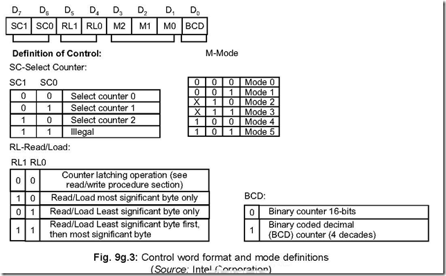
11. Write down the Control Word format as also the mode definitions.
Ans. The details of the control word format, as also the mode definitions are detailed below:
The information stored in the control word gives the following details:
z Bits D7 and D6 (SC1 and SC0) select a counter.
z Bits D5 and D4 (RL1 and RL0) determine whether it is a Read or Load Count operation
and also whether it is Least Significant Byte or Most Significant Byte of the count that
is involved.
z Bits D3, D2, D1 (M2, M1, M0) determine the operating mode (i.e., Mode 0 to Mode 5)
z Bit D0 (BCD) determines the counting sequence in binary or BCD format.
12. How to ensure that a counter is loaded? Ans. For the above to be ensured, it is necessary that:
z The count value be written (a single byte or double byte—which depends on the mode selection by RL1 and RL0 bits).
z The above is then to be followed by a rising and a falling edge of the clock. Data, read before the falling edge of the clock, is an invalid one.
13. How writing operation is done in a counter (i.e., counter 0 or 1 or 2)? Ans. First the control word register is selected.
Secondly, the control word is to be appropriately chosen/written by
(a) selecting the counter in which writing is to be done (D7 – D6 bits).
(b) filling in D5 – D4 bits correctly (which takes care of 1 or 2 byte count).
(c) filling in D3 – D1 bits, which corresponds to Mode selection.
(d) filling in D0 bit—its content reflects the count down to be done in binary/BCD.
14. What will be the Control word register address if CS of 8253 is connected to
A7 via an inverter.
Ans. Since CS pin of 8253 is connected to A7 via an inverter, then A7 will have to be 1, i.e.,
A7 = 1. Again A1 and A0 will both have to be 1 to ensure writing in the control register. Assuming A6 to A2 to be 0, then the port address of the control word register will be
|
A7 |
A6 |
A5 |
A4 |
A3 |
A2 |
A1 |
A0 |
||
|
1 |
0 |
0 |
0 |
0 |
0 |
1 |
1 |
= |
83H |
15. Write the value of the control word if in a specific case counter 0 is to be selected in Mode 1. The counter should have a 16-bit count and that it should count down in binary. Lastly load the control word register with the control word value so formed. Assume address of control word register = 83H.
Ans. Control word for load operation is as follows:
The program for loading the control word value 32H in the control register address 83H is as follows:
MVI A, 32H = Control word is loaded in accumulator
OUT 83H = The control word (= 32H) is written into the control word register, having address 83H.
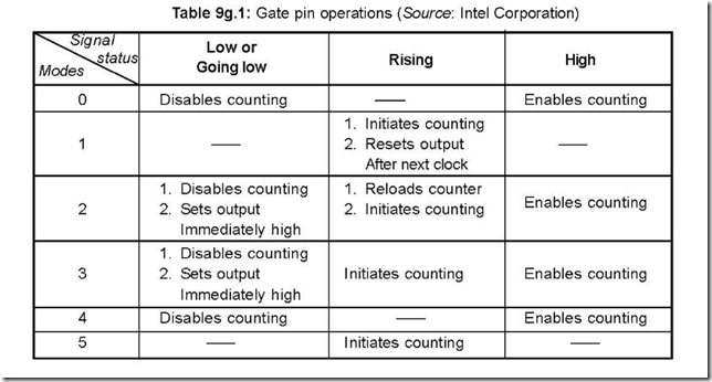
16. Show in a tabular form the conditions of the different Modes corresponding to the different status of the Gate signal.
Ans. This is shown below in a tabular form:
17. Discuss the two methods of reading the value of the count in a counter while count is in progress.
Ans. There are two methods of doing the same
(a) Reading by halting/stopping the count
(b) Reading while counting is ‘ON’ (i.e., counting is in progress)
(a) Reading by halting: The procedure is as follows:
(i) The counter must be identified with appropriate A1 A0 status.
(ii) The counter is then halted by either disabling the Gate pin or inhibiting the
CLK input.
(iii) Then I/O read operation is done—the first I/O Read gets the LSB and the second
I/O Read gets the MSB.
(b) Reading while counting is in progress: For this to be effective, the mode register is loaded with a code that would load the present count (in a counter) to be latched on to a storage register.
The Mode Register Format for Latching Count is as follows:
D5 – D4 are loaded with 0 each for latching the present counter content.
Then the Read command is invoked to the selected counter which gives the content
of the latched register—the counter must be programmed for two bytes and must be read
prior to any Write Command to the concerned counter.


