MICROCONTROLLER IMPLEMENTATIONS
The final stage of a digital control system design is the implementation of the controller algorithm (set of difference equations) on a digital computer. In this section, we shall explore the implementation of digital controller algorithms on PIC microcontrollers. The PIC 16F877 microcontroller will be used in the examples since this microcontroller has a built-in A/D converter and a reasonable amount of program memory and data memory. There are many other microcontrollers in the PIC family with built-in A/D converters, and in general any of these can be used since the operation of microcontrollers in the PIC family with similar features is identical.
Microcontrollers have traditionally been programmed using the assembly language of the target hardware. Assembly language has several important disadvantages and is currently less popular than it used to be. One important disadvantage is that the code generated using the assembly language can only run on the specific target hardware. For example, the assembly program developed for a PIC microcontroller cannot be used, say, on an Intel 8051 micro- controller. Assembly language programs also tend to be more difficult to develop, test and maintain.
In this section, the Hi-Tech PICC language as described in Chapter 4 is used in the imple- mentation of the algorithms. As described in Section 1.6 there are several methods that can be used to implement the controller algorithm. One of the most common, which has the advantage of accurate implementation, is the use of a timer interrupt to generate the required loop delay (or the sampling interval). In this method the software consists of two parts: the main pro- gram and the interrupt service routine. As shown in Figure 10.15(a) Figure 10.15, in the main program various variables, as well as the A/D converter and the timer interrupt mechanism, are initialized. The timer is set to interrupt at an interval equivalent to the sampling interval of the required digital controller. The main program then enters a loop waiting for the timer interrupts to occur. Whenever a timer interrupt occurs the program jumps the interrupt service
routine (ISR) as shown in Figure 10.15(b), and it is within this routine that the actual controller algorithm is implemented. The error signal is obtained by calculating the difference between the reference values and measured values. The algorithm is then implemented and the output sample for the current sampling time is obtained. A preprocessing step is then performed by updating the variables for the next sample. On return from the ISR, the program waits in the main program until the next sampling interval, and the above process repeats.
10.5.1 Implementing Second-Order Modules
In Section 10.2 we saw how a second-order module can be realized using adders, multipliers and delay elements. The second-order module is shown in Figure 10.16. The difference equations describing such a module are (10.19) and (10.20). If we let
The implementation of the second-order module is shown as a flow-chart in Figure 10.17. This figure does not show the initialization of the variables T1, T2, r1, r2, the A/D initialization,
the I/O port initialization, etc.; it only shows the interrupt service routine. A PIC microcon- troller program for the implementation of a second-order module is given in the following example.
Example 10.6
The circuit diagram of a digital control system is shown in Figure 10.18. A PIC16F877 micro- controller is to be used as the digital controller in this system. Assume that the set-point input s is to be hard-coded to the program, and the output y is analog and connected to A/D channel AN0 (bit 0 of port A) of the microcontroller. The microcontroller is assumed to operate with a crystal frequency of 4 MHz as shown in the figure. The output (port B) of the microcontroller is interfaced to a D/A converter which acts as a zero-order-hold and generates an analog output to drive the plant.
Solution
The controller hardware is based on a PIC16F877 microcontroller. The microcontroller is operated from a 4 MHz crystal, connected to OSC1 and OSC2 inputs. With a 4 MHz crystal, the basic clock rate of the microcontroller is 1µs (the crystal frequency is divided by 4 to obtain the basic timing rate). The analog output of the plant (y) is connected to A/D converter channel AN0 of the microcontroller. Similarly, port B digital outputs of the microcontroller are connected to an AD7302 type D/A converter. The operation of this D/A converter is very simple. Digital data is applied to eight inputs D0–D7, while the write control input, WR, is at logic high. The analog data appears at the output after the WR input is lowered to logic low. The WR input of the D/A converter is controlled from port pin RC0 of the microcontroller. The D/A converter is set to operate with a full-scale reference voltage of +5 V. The resolution of the converter is 8 bits, i.e. there are 28 = 256 quantization levels. With a full-scale reference voltage of +5 V,
the resolution is 5000/256 = 19.53 mV, i.e. the digital bit pattern ‘00000001’ corresponds to 19.53 mV, the bit pattern ‘00000010’ corresponds to 2 × 19.53 = 39.06 mV and so on.
The first program attempt is shown in Figure 10.19. Comments are used to describe operation of various parts of the program. The program consists of the main program and the functions: Initialize AD, Initialize Timer, Read AD Input, and ISR.
Main program. The coefficients of the controller are defined at the beginning of the main program. Also, the A/D converter and the timer initialization functions are called here. The main program then enables global interrupts and enters an endless loop waiting for timer interrupts to occur.
ISR. This is the interrupt service routine. The program jumps to this function every 10 ms. The function reads a sample, and calculates the error term ek . The output value yk is then calculated and sent to the D/A converter. In the final part of the ISR, the variables are updated for the next sample, and the timer interrupt is re-enabled.
![]() Initialize Timer. This function initializes the timer TMR0 so that timer interrupts can be generated at 10 ms intervals. As described in Chapter 3, the timing interval depends on the clock frequency, the pre-scaler value, and the data loaded into the TMR0 register. It can be shown that the timing interval is given by:
Initialize Timer. This function initializes the timer TMR0 so that timer interrupts can be generated at 10 ms intervals. As described in Chapter 3, the timing interval depends on the clock frequency, the pre-scaler value, and the data loaded into the TMR0 register. It can be shown that the timing interval is given by:
Initialize AD. This function initializes the A/D converter so that analog data can be received from channel AN0 of the microcontroller. As described in Chapter 3, the A/D converter is initialized by first selecting the reference voltage and the output data format using the ADCON1 register, and then selecting the A/D converter clock using the ADCON0 register. Thus, channel AN0 is configured by loading 0x8E into the ADCON1 register, and 0x41 into the ADCON0 register. Thus, the Initialize AD function is programmed as follows:
Read AD Input. This function starts the A/D converter and reads a sample at the end of the conversion. The conversion is started by setting the GO/DONE bit of ADCON0. The program should then wait until the conversion is complete, which is indicated by the GO/DONE bit becoming zero. The high 2 bits of the converted data are in ADRESH, and the low 8 bits are in register ADRESL. The 10-bit converted data is extracted and stored in variable yk .
Implementing First-Order Modules
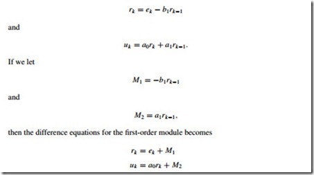
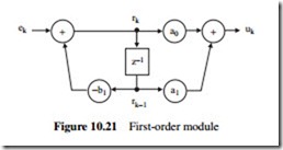
In Section 10.2 we saw how a first-order module can be realized using adders, multipliers and delay elements. The first-order module is shown in Figure 10.21. The difference equations describing a first-order module were found to be
The implementation of the first-order module is similar to the second-order module and an example is given below.
Example 10.7
The circuit diagram of a digital control system is shown in Figure 10.18. A PIC16F877 micro- controller is to be used as the digital controller in this system. Assume that the set-point input s is to be hard-coded to the program, and the output y is analog and connected to A/D channel AN0 (bit 0 of port A) of the microcontroller. The microcontroller is assumed to operate with a crystal frequency of 4 MHz as shown in the figure. The output (port B) of the microcontroller is interfaced to a D/A converter which acts as a zero-order-hold and generates an analog output to drive the plant.
Assume that the digital controller to be implemented is in the form of a first-order module, and write a program in C to implement this controller. The controller parameters are assumed to be:
Solution
The implementation of a first-order module is very similar to a second-order module. The program to implement a first-order controller is shown in Figure 10.22. The operation of the program is very similar to the second-order program and is not described here.
Implementing Higher-Order Modules
Higher-order controllers can be implemented by cascading first-order and second-order mod- ules. For example, a fourth-order controller can be implemented by cascading two second-order modules, as shown in Figure 10.23.


