PROJECT 21 – Using Analogue Temperature Sensor IC with A/D Converter
Function
This project shows how we can connect an analogue-to-digital (A/D) converter IC to our microcontroller. In this project, an analogue temperature sensor IC (LM35DZ) is used and its output is connected to an 8-bit A/D converter (ADC0804). The temperature is then displayed every second on a TSM5034 type 4-digit display. The block diagram of this project is shown in Fig. 5.I2.
The A/D converter shown in this project can be connected to any kind of analogue voltage. For example, a digital voltmeter can be constructed easily by connecting the A/D converter input to an external voltage which is to be measured.
Circuit Diagram
Before looking at the circuit diagram of this project, it will be useful if we look at the ways an A/D converter can be connected to a microcontroller. There are many types of A/D converters available on the market. Some converters provide serial output data such that the output data is obtained from the converter each time a clock pulse is sent to the converter. These converters are very slow and are generally used where the speed of conversion is not important and where space saving is required. Serial A/D converters interface to a microcontroller by using only a few pins.
Standard A/D converters are generally used in medium- and high-speed applications. An example of such an A/D converter is the ADC0804,
manufactured by the National Semiconductor Corporation. The conversion time of this A/D converter is I00 !ls. As shown in Fig. 5.I3, these converters interface to the microcontroller using the following pins (only the pins used in a standard application are shown):
RD is the read data control pin and when RD is low (logic 0), output data appears on the eight output pins. When RD is high (logic I), the output is not available.
WR input is normally at logic high and this input should be set to low and then high again for a conversion to start.
INTR is the interrupt output of the A/D converter. A high to low pulse is generated on this pin when a conversion is complete. This output is usually used to generate an interrupt in the microcontroller so that the converted data can be read.
ADC0804 contains an internal oscillator and it is required to connect an external resistor and a capacitor to pins CLK R and CLK IN to start the oscillator.
VIN+ is the pin where the analog input voltage should be applied.
• Set WR and RD high
• Start conversion by setting WR low
• Set WR back tohigh
• Detect end of conversion when INTR goes low (usually by interrupt)
• Set RD low and read data from DB0 to DB7
• Set RD high
The above process is of course repeated when more than one conversion is required.
Figure 5.I4 shows the full circuit diagram of Project 2I. Data and clock inputs of the TSM5034 are connected to bits I and 0 of port 3 respectively. The eight
data outputs of the ADC0804 are connected to port I. RD input is connected to bit 2 of port 3. WR is connected to bit 4 of port 3. The interrupt output, INTR, of the A/D converter is connected to bit 3 of port 3 which is the external interrupt I (INTI) pin of the microcontroller. Analogue input voltage is applied to pin 6 of the A/D converter and this input can be connected to any kind of analogue voltage which is to be measured.
In this project, analogue data comes from an LM35DZ type IC analogue temperature sensor. LM35DZ is a simple temperature sensor IC. Pin I of the device is connected to a power supply (e.g. +5 V), pin 3 is connected to the ground. Pin 2 is the output and this output provides a voltage which is directly proportional to the measured temperature. The device can measure tempera- tures from 2oC up toI00oC (some types can measure a wider range) and the output voltage to temperature relationship is I0 mV/oC. For example, at 20oC the output is 200 mV. Similarly, at 35oC, the output voltage is 350 mV, and so on. Internal oscillator of the A/D converter is activated by connecting an external resistor and a capacitor to pins CLK R and CLK IN. Notice that bits 0 and I of port I are connected to +5 V using pull-up resistors. This is necessary in some applications since the output drivers at these pins are open drain (i.e. there are nointernal pull-up resistors).
Program Description
The display part of the program is as described in the light pro}ects section of the book. We shall therefore look at the way the A/D converter is controlled by the software. The following PDL describes the operation of the project:
The program clears the display and then initializes the microcontroller so that external interrupts on pin INTI can be recognized. The A/D is then initialized and the conversion started. At the end of a conversion, an interrupt is generated by the A/D converter and execution jumps to the INTI service routine. Here, the converter data is read and displayed on the TSM5034 display. At the same time a new conversion is restarted.
Program Listing
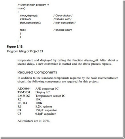
The complete program listing is shown in Fig. 5.I5. Display clock and display data variables are assigned to pins 0 and I, respectively, of port 3 of the microcontroller. Similarly, A/D RD and A/D WR variables are assigned to pins 2 and 4 of port 3 of the microcontroller. When the program starts it first clears the display. Function initialize is then called toset the A/D RD and WR inputs (ADC_RD and ADC_WR) toI. External interrupt pin INT1 of the microcontroller is also set (IT1 = 1) in this routine to accept interrupts on high- to-low transition and the microcontroller is configured to accept interrupts (EA = 1). Function start_conversion is then called to start an A/D conversion. This function simply sets the WR input of the A/D to0 and then back toI. The program then enters an endless loop and waits for external interrupts on its INT1 pin.
INT1 has the interrupt number of 2. When a conversion is complete, control passes tothe interrupt service routine int1. In this routine, RD input of the A/D converter is set to 0 to enable the output buffers and then the digital data is read into port I of the microcontroller. The value read is then converted to true


