Analogue Input
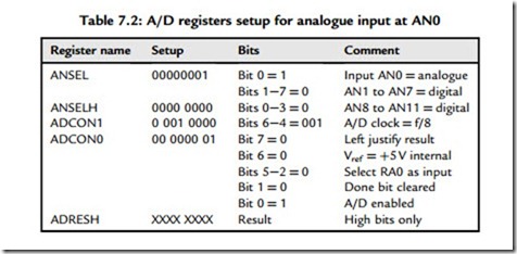
The registers used in setting up and operating the analogue input are listed in Table 7.2.
The ANSEL and ANSELH (analogue input select) register bits are configured with 0 for digital and 1 for analogue inputs. Only AN0 is required in this case (ANSEL,0), the others will be set for digital input. The register bits default to 1, or analogue inputs, so must be initialized for digital I/O with 0. Usually it is convenient to clear all the control bits, and then setthose that are required as analogue inputs.
The analogue-to-digital converter (ADC) works by a successive approximation method, and uses the system clock to drive the converter that generates the binary equivalent of the input voltage. Since the conversion takes a minimum time per bit, the clock must not be too fast, so a frequency divider is provided which can be set to a suitable value. The recommended division ratio is given in the data sheet (Table 9-1) for each oscillator frequency. In this example, a 4 MHz system clock requires division by 8, to provide a 500 kHz A/D clock. ADCON1, bits 4, 5 and 6 are used to select the recommended ADC clock rate.
ADCON0 has several functions. ADCON0,0 enables the ADC and bit 1 starts the conversion process when set to 1 in the program, and also indicates the conversion is finished when it is cleared in hardware. In the test program, this bit is polled in a loop that repeats until it is cleared. Bits 2e5 select the current input as the corresponding binary number (0000 ¼ AN0,
The ADC needs a reference voltage to set the range of the input that will be converted. ANCON0,6 selects between an internal reference of 5 V and an external reference which must be supplied from a constant voltage circuit, usually based on a zener diode. A 10-bit conversion gives results from 0000000000 (010) to 1111111111 (102310) or 1024 steps, giving a resolution of better than 0.1%. If an accurate reference voltage of say 4.096 V is supplied, the resolution will be 4096/1024 ¼ 4.00 mV per bit. With a 5 V reference, the resolution would not be such a convenient value (5000/1024 ¼ 4.88 mV), but no external circuit is needed. In the test program, an accurate measurement is not needed, so the internal reference is used.
Since the result is more than 8 bits, two registers are needed to receive the result: ADRESH and ADRESL. The justification of the result controls how it is placed in these. Left justification places the high 8 bits in ADRESH and the low 2 bits in ADRESL (bits 6 and 7). In the test program, therefore, the whole range is covered (0e5 V) by reading ADRESH, but at reduced 8-bit resolution (19.5 mV per bit). Right justification places the low 8 bits in ADRESL, providing 25% of the range (0e1.25 V) but at full resolution.
