Peripheral Interfaces
In the block diagram of each chip, the peripherals are shown as separate blocks attached to the internal data bus. These provide additional features such as timers, analogue inputs and serial ports. These are set up for use by initializing the related SFRs. The appropriate combination of peripherals is a major factor in chip selection.
Timers and CCP
Hardware timers are used for timing and counting operations, allowing the processor to carry on with some other process while the timer process runs. Basic timer operation has been described in Chapter 6, where a clock input drives a counting register to measure time or count external events. Its functionality can be extended by using additional registers to store timer values, creating a CCP module. CCP stands for capture/compare/PWM.
Capture mode provides input interval measurement (Figure 12.4a). The value in a timer register is captured (stored) when an input changes; the time between the timer start and input change is therefore recorded. In the motor application, for example, the timer could be started when a pulse is received from the shaft sensor, and the time captured when the next pulse arrives, giving the period of the shaft sensor pulse. An interrupt can be enabled to signal this event.
Compare mode provides output interval generation (Figure 12.4b). A value is loaded into a register, which is then continuously compared with a timer register as it runs. When the register values match, an output pin is toggled and an interrupt generated to signal the timeout event. This is a convenient way to generate a timed interval, so that, for example, an output pulse waveform can be generated with set pulse period.
In PWM mode, preset values are loaded into two registers representing the mark and space period of the PWM output required (Figure 12.5). The timer value is then compared with the mark register and the output toggled after the mark value is reached. The timer is then restarted and compared with the space value as it runs, and the output toggled when the space value matches. The process is repeated, causing the output from the flip-flop to toggle after each mark and space interval, generating a PWM output.
Analogue Comparators
The comparator allows one voltage to be compared with another, and sets or clears its output bit depending on the polarity of the input. Many PICs incorporate comparator inputs as well as analogue/digital (A/D) inputs, with the result bits recorded in a relevant SFR. Often, there are multiple inputs which can be set up to operate in different combinations, and also trigger a range of output events, such as an interrupt. See, for example, the block diagram of the 16F690 C1 comparator module (Figure 8-2 in the data sheet).
Analogue/Digital Inputs
The analogue inputs are used in control systems with input sensors that produce a voltage, current or resistance change in response to an environmental variation or system measurement. For example, in the LPC board, a pot is connected to RA0, which is designated AN0 when used as an analogue input. In the test program, it reads 0e5 V from the pot and uses this value to control the speed of the LED output scan, by copying it into the delay counter as the initial value. The temperature controller described in Chapter 13 is designed to accept inputs from temperature sensors which give an output change of 10 mV/oC. The PIC then operates outputs to a heater or a cooling fan, which keep the temperature in the target system constant.
Most PICs provide 10-bit conversion. This means that the input voltage is converted to a 10-bit number, giving a resolution of 1 in 1024, or better than 0.1%. This is good enough for all but the most demanding applications. If the full resolution is not required, an 8-bit result can be used by ignoring the two extra bits. Multiple analogue inputs are usually available; the PIC 16F690 has 12 (AN0 to AN11). Code for performing the analogue input conversion is given in the LPC Program 7.1.
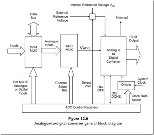
The analogue-to-digital conversion (ADC) system is illustrated in Figure 12.6. The port containing the ADC inputs can be set up with a combination of analogue and digital inputs, or all analogue. One of the analogue inputs is selected at a time for conversion, and the converter output is stored in an ADC result register. The maximum voltage level to be converted (reference voltage) can be set externally, or the internal supply voltage (þ5 V) can be used. In the temperature controller board, an external voltage reference of þ2.56 V is used, because this gives a convenient 0.01 V per bit conversion for an 8-bit result. The converter is driven by the chip clock, but a divider must be set up to allow the minimum specified conversion time (about
20 ms); for example, if the chip clock is 20 MHz, divide by 32 must be selected, and at 4 MHz, divide by 8. The GO/DONE bit in the control register is used to start a conversion; the same bit indicates when the conversion is finished.
The ADC works by successive approximation, details of which can be found in standard electronics references. The converter consists of a register, a digital-to-analogue converter (DAC) and an analogue comparator. The register is loaded with the half-range value (512 for 10 bits) and this is converted to an analogue value by the DAC, whose maximum output is set by the ADC reference voltage. The DAC output voltage is compared with the input, and if the input is higher, the comparator value is increased by half of the remaining range (512 þ 256 ¼ 768, set bit 8). The input is compared again and the register value adjusted up or down, until the value converges on the actual input value within 10 iterations.


