Input/Output Pins
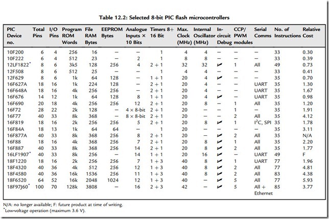
The number and type of inputs and outputs required needs to be considered at an early stage in circuit design. The convenient grouping of the pins for particular interfaces may also be relevant, with many chips having partial port implementations. For example, a 4-bit port can be conveniently used for a 4-bit input from a DIL switch, while a seven-segment display with a decimal point needs the full 8-bit port. The number of analogue inputs available must also be adequate for inputs requiring a voltage measurement. Most I/O pins have more than one function, one of which is selected during initialization by setting up the relevant control register. If no setup is performed for a particular pin, it will normally default to a digital input, or an analogue input if this is an option. Pins can be reconfigured within the program sequence to have a different function at different times. If this is the case, the designer must ensure that the two functions do not interfere with each other, in terms of both the hardware and the software.
Program Memory
The specification of memory size can only be finalized after the software has been developed, but an experienced application developer should be able to anticipate this requirement fairly early on. Otherwise, a chip with more than enough memory can be used at first, and one with the correct capacity selected later on. If the program is developed in ‘C’ language, the memory size required will be greater, because each program statement can expand into several machine code instructions. In this case, an 18 series device is likely to be the best choice. Microchip supply a free C compiler for the 18XXXX chips, and third party compilers are also available for both the 18 and 16 series chips. PIC microcontrollers are generally supplied with flash program memory, as this is the most flexible option for prototyping and production. If larger volumes of chips with a fixed program are required, masked ROM program memory (not reprogrammable) can be configured in the final manufacturing stage.
Data Memory
The file register RAM block, which includes the SRFs and GPRs, tends to increase in size with the program memory size and chip complexity, and ranges from 16 to 4096 bytes in the 8-bit PICs. Note that some blocks of RAM are unique, while others are common to all the RAM banks (that is, the same register is accessed at the corresponding address in different banks), while other address ranges may not be implemented at all. Therefore, the total amount of RAM cannot simply be calculated as the number of locations per bank multiplied by the number of banks. For example, the 16F690 has four banks of 128 locations, equivalent to 512 addresses. The first 32 addresses in each bank are assigned as SFRs (total 128), but there are only 256 bytes in total of unique RAM locations (20he7Fh, A0heEFh and 120he16Fh). The remaining 128 registers are duplicates or unimplemented. The number of variables and temporary data storage blocks required can be totaled when the program has been developed, perhaps adding an allowance for future expansion or changes to the specification. If non-volatile data storage is needed, the EEPROM size must also be checked.
Internal Oscillators
To save on external components, many PICs now include an internal oscillator. In the ’690, this runs at 8 MHz, or lower frequencies by division, with a default of 4 MHz selected if the OSCCON register is not initialized and the internal oscillator selected in the configuration word. More recently, 32 MHz internal oscillators have been introduced. The frequency can be calibrated using an internal register if a more accurate clock is needed. However, an external crystal clock will still provide maximum accuracy. In recent chips, multiple clock modes are available to optimize the tradeoff between clock speed, accuracy and power consumption. Many chips now have an additional internal oscillator, an internal 31 kHz clock, which can be connected to Timer 1 as an independent timebase and drives the power-up timer system.
Clock Speed
Clock speed is the primary factor in the performance of any microprocessor system, and is critical in some applications. For example, in the motor control example previously described, the higher the clock speed, the more precise the control can be, as the shaft speed can potentially be measured more accurately. Most of the flash PICs currently available operate at up to 20 MHz (12 and 16 series) or 40 MHz (18 series). This gives an instruction cycle time of 200 or 100 ns (nanoseconds) and an execution rate of 5 or 10 MIPS (million instructions per second). All PICs use a fully static design, which means that they can operate down to zero frequency. The clock rate is limited by the time taken by the internal signals to rise and fall, so correct performance is only guaranteed up to the maximum rated speed. The maximum speed is also limited by power dissipation and the consequent heating effect.

