INTRODUCTION TO THE PENTIUM PRO MICROPROCESSOR
Before this or any other microprocessor can be used in a system, the function of each pin must be understood. This section of the chapter details the operation of each pin, along with the external memory system and I/O structures of the Pentium Pro microprocessor.
versions: One version contains a 256K level 2 cache; the other contains a 512K level 2 cache. The most notable difference in the pin-out of the Pentium Pro, when compared to the Pentium, is that there are provisions for a 36-bit address bus, which allows access to 64G bytes of memory. This is meant for future use because no system today contains anywhere near that amount of memory.
As with most recent versions of the Pentium microprocessor, the Pentium Pro requires a single +3.3 V or +2.7 V power supply for operation. The power supply current is a maximum of 9.9 A for the 150 MHz version of the Pentium Pro, which also has a maximum power dissipation of 26.7 W. A good heat sink with considerable airflow is required to keep the Pentium Pro cool. As with the Pentium, the Pentium Pro contains multiple VCC and VSS connections that must all be connected for proper operation. The Pentium Pro contains VCCP pins (primary VCC) that connect to +3.1 V, VCCS (secondary VCC) pins that connect to +3.3 V, and VCC5 (standard VCC) pins that connect to +5.0 V. There are some pins that are labeled N/C (no connection) and must not be connected.
Each Pentium Pro output pin is capable of providing an ample 48.0 mA of current at a logic 0 level. This represents a considerable increase in drive current, compared to the 2.0 mA available on earlier microprocessor output pins. Each input pin represents a small load, requiring only 15 μA of current. Because of the 48.0 mA of drive current available on each output, only an extremely large system requires bus buffers.
Internal Structure of the Pentium Pro
The Pentium Pro is structured differently than earlier microprocessors. Early microprocessors contained an execution unit and a bus interface unit with a small cache buffering the execution unit for the bus interface unit. This structure was modified in later microprocessors, but the modifications were just additional stages within the microprocessors. The Pentium architecture is also a modification, but more significant than earlier microprocessors. Figure 18–13 shows a block diagram of the internal structure of the Pentium Pro microprocessor.
The system buses, which communicate to the memory and I/O, connect to an internal level 2 cache that is often on the main board in most other microprocessor systems. The level 2 cache in the Pentium Pro is either 256K bytes or 512K bytes. The integration of the level 2 cache speeds processing and reduces the number of components in a system.
The bus interface unit (BIU) controls the access to the system buses through the level 2 cache, as it does in most other microprocessors. Again, the difference is that the level 2 cache is integrated. The BIU generates the memory address and control signals, and passes and fetches data or instructions to either a level 1 data cache or a level 1 instruction cache. Each cache is 8K bytes in size at present and may be made larger in future versions of the microprocessor. Earlier versions of the Intel microprocessor contained a unified cache that held both instructions and data. The implementation of separate caches improves performance because data-intensive pro- grams no longer fill the cache with data.
The instruction cache is connected to the instruction fetch and decode unit (IFDU). Although not shown, the IFDU contains three separate instruction decoders that decode three instructions simultaneously. Once decoded, the outputs of the three decoders are passed to the instruction pool, where they remain until the dispatch and execution unit or retire unit obtains them. Also included within the IFDU is a branch prediction logic section that looks ahead in code sequences that contain conditional jump instructions. If a conditional jump is located, the branch prediction logic tries to determine the next instruction in the flow of a program.
Once decoded instructions are passed to the instruction pool, they are held for processing. The instruction pool is a content-addressable memory, but Intel never states its size in the literature.
The dispatch and execute unit (DEU) retrieves decoded instructions from the instruction pool when they are complete, and then executes them. The internal structure of the DEU is
illustrated in Figure 18–14. Notice that the DEU contains three instruction execution units: two for processing integer instructions and one for floating-point instructions. This means that the Pentium Pro can process two integer instructions and one floating-point instruction simultaneously. The Pentium also contains three execution units, but the architecture is different because the Pentium does not contain a jump execution unit or address generation units, as does the Pentium Pro. The reservation station (RS) can schedule up to five events for execution and process four simultaneously. Note that there are two station components connected to one of the address generation units that does not appear in the illustration of Figure 18–14.
The last internal structure of the Pentium Pro is the retire unit (RU). The RU checks the instruction pool and removes decoded instructions that have been executed. The RU can remove three decoded instructions per clock pulse.
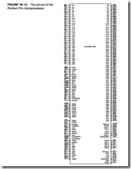
The number of pins on the Pentium Pro has increased from the 237 pins on the Pentium to 387 pins on the Pentium Pro. Following is a description of each pin or grouping of pins:
A20M
The address A20 mask is an input that is asserted in the real mode to signal the Pentium Pro to perform address wraparound, as in the 8086 microproces- sor, for use of the HIMEM.SYS driver.
Address bus connections address any of the 8G × 64 memory locations found in the Pentium Pro memory system.
The address data strobe becomes active whenever the Pentium Pro has issued a valid memory or I/O address.
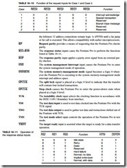
Address parity provides even parity for the memory address on all Pentium Pro–initiated memory and I/O transfers. The AP0 output provides parity for address connections A23–A3, and the AP1 output provides parity for address connections A35–A24.
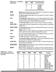
Address size inputs are driven to select the size of the memory access. Table 18–6 illustrates the size of the memory access for the binary bit patterns on these two inputs to the Pentium Pro.
BCLK The bus clock input determines the operating frequency of the Pentium Pro microprocessor. For example, if BCLK is 66 MHz, various internal clocking speeds are selected by the logic levels applied to the pins in Table 18–7. A BCLK frequency of 66 MHz runs the system bus at 66 MHz.
BERR
The bus error input/output either signals a bus error along or is asserted by an external device to cause a machine check interrupt or a non-maskable interrupt.
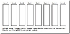
The memory system for the Pentium Pro microprocessor is 4G bytes in size, just as in the 80386DX–Pentium microprocessors, but access to an area between 4G and 64G is made possible by additional address signals A32–A35. The Pentium Pro uses a 64-bit data bus to address memory organized in eight banks that each contain 8G bytes of data. Note that the additional memory is enabled with bit position 5 of CR4 and is accessible only when 2M paging is enabled. Note also that 2M paging is new to the Pentium Pro to allow memory above 4G to be accessed. More information is presented on Pentium Pro paging later in this chapter. Refer to Figure 18–15 for the organization of the Pentium Pro physical memory system.
The Pentium Pro memory system is divided into eight banks where each bank stores a byte-wide data with a parity bit. Note that most Pentium and Pentium Pro microprocessor-based systems forgo the use of the parity bit. The Pentium Pro, like the 80486 and Pentium, employs internal parity generation and checking logic for the memory system data bus information. The 64-bit-wide memory is important to double-precision floating-point data. Recall that a double- precision floating-point number is 64 bits wide. As with earlier Intel microprocessors, the memory system is numbered in bytes from byte 000000000H to byte FFFFFFFFFH. This nine-digit hexadecimal address is employed in a system that addresses 64G of memory.
Memory selection is accomplished with the bank enable signals (BE7–BE0). In the Pentium Pro microprocessor, the bank enable signals are presented on the address bus (A15–A8) during the second clock cycle of a memory or I/O access. These must be extracted from the address bus to access memory banks. The separate memory banks allow the Pentium Pro to access any single byte, word, doubleword, or quadword with one memory transfer cycle. As with earlier memory selection logic, we often generate eight separate write strobes for writing to the memory system. Note that the memory write information is provided on the request lines from the microprocessor during the second clock phase of a memory or I/O access.
A new feature added to the Pentium and Pentium Pro is the capability to check and generate parity for the address bus during certain operations. The AP pin (Pentium) or pins (Pentium Pro) provide the system with parity information, and the APCHK (Pentium) or AP pins (Pentium Pro) indicate a bad parity check for the address bus. The Pentium Pro takes no action when an address-parity error is detected. The error must be assessed by the system, and the system must take appropriate action (an interrupt) if so desired.
New to the Pentium Pro is a built-in error-correction circuit (ECC) that allows the correction of a one-bit error and the detection of a two-bit error. To accomplish the detection and
correction of errors, the memory system must have room for an extra 8-bit number that is stored with each 64-bit number. The extra 8 bits are used to store an error-correction code that allows the Pentium Pro to automatically correct any single-bit error. A 1M × 64 is a 64M SDRAM without ECC, and a 1M × 72 is an SDRAM with EEC support. The ECC code is much more reliable than the old parity scheme, which is rarely used in modern systems. The only drawback of the ECC scheme is the additional cost of SDRAM that is 72 bits wide.
Input/Output System
The input/output system of the Pentium Pro is completely compatible with earlier Intel micro- processors. The I/O port number appears on address lines A15–A3 with the bank enable signals used to select the actual memory banks used for the I/O transfer.
System Timing
As with any microprocessor, the system timing signals must be understood in order to interface the microprocessor. This portion of the text details the operation of the Pentium Pro through its timing diagrams and shows how to determine memory access times.
The basic Pentium Pro memory cycle consists of two sections: the address phase and the data phase. During the address phase, the Pentium Pro sends the address (T1) to the memory and I/O system, and also the control signals (T2). The control signals include the ATTR lines (A31–A24), the DID lines (A23–A16), the bank enable signals (A15–A8), and the EXF lines (A7–A3). See Figure 18–16 for the basic timing cycle. The type of memory cycle appears on the request pins. During the data phase, four 64-bit-wide numbers are fetched or written to the memory. This operation is most common because data from the main memory are transferred between the internal 256K or 512K write-back cache and the memory system. Operations that write a byte, word, or doubleword, such as I/O transfers, use the bank selection signals and have only one clock in the data transfer phase. Notice from the timing diagram that the 66 MHz Pentium Pro is capable of 33 million memory transfers per second. (This assumes that the memory can operate at that speed.)
The setup time before the clock is given as 5.0 ns and the hold time after the clock is given as 1.5 ns. This means that the data window around the clock is 6.5 ns. The address appears on the ns maximum after the start of T1. This means that the Pentium Pro microprocessor operating at 66 MHz allows 30 ns (two clocking periods), minus the address delay time of 8.0 ns and also


