THE PERIPHERAL COMPONENT INTERCONNECT (PCI) BUS
The PCI (peripheral component interconnect) bus is virtually the only bus found in the newest Pentium 4 systems and just about all the Pentium systems. In all of the newer systems, the ISA bus still exists by special order, but as an interface for older 8-bit and 16-bit interface cards. Many new systems contain only two ISA bus slots or no ISA slots. In time, the ISA bus may dis- appear, but it is still an important interface for many industrial applications. The PCI bus has replaced the VESA local bus. One reason is that the PCI bus has plug-and-play characteristics and the ability to function with a 64-bit data bus. A PCI interface contains a series of registers, located in a small memory device on the PCI interface, that contain information about the board. This same memory can provide plug-and-play characteristics to the ISA bus or any other bus. The information in these registers allows the computer to automatically configure the PCI card. This feature, called plug-and-play (PnP), is probably the main reason that the PCI bus has become so popular in the most systems.
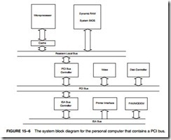
Figure 15–6 shows the system structure for the PCI bus in a personal computer system. Notice that the microprocessor bus is separate and independent of the PCI bus. The microprocessor
connects to the PCI bus through an integrated circuit called a PCI bridge. This means that virtually any microprocessor can be interfaced to the PCI bus, as long as a PCI controller or bridge is designed for the system. In the future, all computer systems may use the same bus. Even the Apple Macintosh system is switching to the PCI bus. The resident local bus is often called a front side bus.
The PCI Bus Pin-Out
As with the other buses described in this chapter, the PCI bus contains all of the system control signals. Unlike the other buses, the PCI bus functions with either a 32-bit or a 64-bit data bus and a full 32-bit address bus. Another difference is that the address and data buses are multiplexed to reduce the size of the edge connector. These multiplexed pins are labeled AD0–AD63 on the connector. The 32-bit card (which is found in most computers) has only connections 1 through 62, while the 64-bit card has all 94 connections. The 64-bit card can accommodate a 64-bit address if it is required at some point in the future. Figure 15–7 on the next page illustrates the PCI bus pin-out.
As with the other bus systems, the PCI bus is most often used for interfacing I/O components to the microprocessor. Memory could be interfaced, but it would operate only at a 33 MHz rate with the Pentium, which is half the speed of the 66 MHz resident local bus of the Pentium system. A more recent version of PCI (2.1-compliant) operates at 66 MHz and at 33 MHz for older interface cards. Pentium 4 systems use a 200 MHz system bus speed (although it is often listed as 800 MHz), but there is no planned modification to the PCI bus speed yet.
The PCI Address/Data Connections
The PCI address appears on AD0–AD31 and it is multiplexed with data. In some systems, there is a 64-bit data bus that uses AD32–AD63 for data transfer only. In the future, these pins can be used for extending the address to 64 bits. Figure 15–8 illustrates the timing diagram for the PCI bus, which shows the way that the address is multiplexed with data and also the control signals used for multiplexing.
During the first clocking period, the address of the memory or I/O location appears on the AD connections, and the command to a PCI peripheral appears on the C>BE pins. Table 15–4 illustrates the bus commands found on the PCI bus.
INTA Sequence During the interrupt acknowledge sequence, an interrupt controller (the controller that caused the interrupt) is addressed and interrogated for the interrupt vector. The byte-sized interrupt vector is returned during a byte read operation.
Special Cycle The special cycle is used to transfer data to all PCI components.
During this cycle, the rightmost 16 bits of the data bus contain a 0000H, indicating a processor shutdown, 0001H for a processor halt, or 0002H for 80X86 specific code or data.
I/O Read Cycle Data are read from an I/O device using the I/O address that appears on AD0–AD15. Burst reads are not supported for I/O devices.
I/O Write Cycle As with I/O read, this cycle accesses an I/O device, but writes data.
FIGURE 15–8 The basic burst mode timing for the PCI bus system. Note that this transfers either four 32-bit numbers (32-bit PCI) or four 64-bit numbers (64-bit PCI).
Memory Read Cycle Data are read from a memory device located on the PCI bus.
Memory Write Cycle As with memory read, data are accessed in a device located on the PCI bus. The location is written.
Configuration Read Configuration information is read from the PCI device using the
configuration read cycle.
Configuration Write The configuration write allows data to be written to the configuration area in a PCI device. Note that the address is specified by the configuration read.
Memory Multiple This is similar to the memory read access, except that it is usually
Access used to access many data instead of one.
Dual Addressing Used for transferring address information to a 64-bit PCI device, Cycle which only contains a 32-bit data path.
Line Memory Used to read more than two 32-bit numbers from the PCI bus.
Addressing
Memory Write with This is the same as line memory access, but it is used with a write.
Invalidation This write bypasses the write-back function of the cache.
Configuration Space
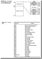
The PCI interface contains a 256-byte configuration memory that allows the computer to interrogate the PCI interface. This feature allows the system to automatically configure itself for the PCI plug-board. Microsoft Corporation calls this plug-and-play (PnP). Figure 15–9 illustrates the configuration memory and its contents.
The first 64 bytes of the configuration memory contain the header that holds information about the PCI interface. The first 32-bit doubleword contains the unit ID code and the vendor ID code. The unit ID code is a 16-bit number (D31–D16) that is an FFFFH if the unit is not installed, and a number between 0000H and FFFEH that identifies the unit if it is installed. The class codes identify the class of the PCI interface. The class code is found in bits D31–D16 of configuration memory at location 08H. Note that bits D15–D0 are defined by the manufacturer. The current
class codes are listed in Table 15–5 and are assigned by the PCI SIG, which is the governing body for the PCI bus interface standard. The vendor ID (D15–D0) is also allocated by the PCI SIG.
The status word is loaded in bits D31–D16 of configuration memory location 04H and the command is at bits D15–D0 of location 04H. Figure 15–10 illustrates the format of both the status and command registers.
The base address space consists of a base address for the memory, a second for the I/O space, and a third for the expansion ROM. The first two doublewords of the base address space contain either the 32- or 64-bit base address for the memory present on the PCI interface. The next doubleword contains the base address of the I/O space. Note that even though the Intel microprocessors only use a 16-bit I/O address, there is room for expanding the I/O address to 32 bits. This allows systems that use the 680X0 family and PowerPC access to the PCI bus because they do have I/O space that is accessed via a 32-bit address. The 600X0 and PowerPC use memory-mapped I/O, discussed at the beginning of Chapter 11.
BIOS for PCI
Most modem personal computers contain the PCI bus and an extension to the normal system BIOS that supports the PCI bus. These newer systems contain access to the PCI bus at interrupt vector 1AH. Table 15–6 lists the functions currently available through the DOS INT 1AH instruction with AH = 0B1H for the PCI bus.
Example 15–5 shows how the BIOS is used to determine whether the PCI bus extension available. Once the presence of the BIOS is established, the contents of the configuration memory can be read using the BIOS functions. Note that the BIOS does not support data transfers between the computer and the PCI interface. Data transfers are handled by drivers that are pro- vided with the interface. These drivers control the flow of data between the microprocessor and the component found on the PCI interface.
PCl Interface
The PCI interface is complex, and normally an integrated PCI bus controller is used for interfacing to the PCI bus. It requires memory (EPROM) to store vendor information and other information, as explained earlier in this section of the chapter. The basic structure of the PCI interface is illustrated in Figure 15–11. The contents of this block diagram illustrate the required components for a functioning PCI interface; it does not illustrate the interface itself. The Registers, Parity Block, Initiator, Target, and Vendor ID EPROM are required components of any PCI interface. If a PCI interface is constructed, a PCI controller is often used because of the complexity of this interface. The PCI con- troller provides the structures shown in Figure 15–11.
PCI Express Bus
The PCI Express transfers data in serial at the rate of 2.5 GHz to legacy PCI applications, increasing the data link speed to 250 MBps to 8 GBps for PCI Express interfaces. The standard PCI bus delivers data at a speed of about 133 MBps, in comparison. The big improvement is on the moth- erboard, where the interconnections are in serial and at 2.5 GHz. Each serial connection on the PCI Express bus is called a lane. The slots on the main board are single lane slots with a total transfer speed of 1 GBps. The PCI Express video card connector currently has 16 lanes with a
transfer speed of 4 GBps. The standard allows up to 32 lanes, but at present the widest slot is the 16 lanes on the video card. Most current main boards contain four single lane slots for peripherals and one 16 lane slot for the video card. A few newer main boards contain two 16 lane slots. In the future the standard PCI slots will all be replaced with the lower cost PCI Express connectors.
The PCI Express 2 bus was released in late 2007 with a transfer speed that is twice that of the PCI Express bus. This means that the speed per lane increased from 250 MBps to 500 MBps.
This new version of the PCI bus is replacing most current video cards on the AGP port with a yet higher speed version of the PCI Express bus. This technology (serial) allows main board manufacturers to use less space on the main board for interconnection and thus reduce the cost of manufacturing a main board. The connectors are smaller, which also reduces connector cost. The software used with the PCI Express bus remains the same as that used with the PCI bus so new programs are not needed to develop drivers for the PCI Express bus.
The PCI Express pin-out for the most commonly interfaced connector, the single lane connector, appears in Table 15–7. The connector is a 36-pin connector as illustrated in Figure 15–12. Signaling on the PCI Express bus uses 3.3 V with differential signals that are 180 degrees
out of phase. The lane is constructed from a pair of data pipes, one for input data and one for output data.


