INTRODUCTION
Many applications require some knowledge of the bus systems located within the personal computer. At times, main boards from personal computers are used as core systems in industrial applications. These systems often require custom interfaces that are attached to one of the buses on the main board. This chapter presents the ISA (industry standard architecture) bus, the PCI (peripheral component interconnect) and PCI Express buses, the USB (universal serial bus), and the AGP (advanced graphics port). Also provided are some simple interfaces to many of these bus systems as design guides.
Although it is likely that they will not be on personal computers of the future, the parallel port and serial communications ports are discussed. These were the first I/O ports on the per- sonal computer and they have stood the test of time, but the universal serial bus seems to have all but replaced their utility.
CHAPTER OBJECTIVES
Upon completion of this chapter, you will be able to:
1. Detail the pin connections and signal bus connections on the parallel and serial ports as well as on ISA, AGP, PCI, and PCI Express buses.
2. Develop simple interfaces that connect to the parallel and serial ports and the ISA and PCI buses.
3. Program interfaces located on boards that connect to the ISA and PCI buses.
4. Describe the operation of the USB and develop some short programs that transfer data.
5. Explain how the AGP increases the efficiency of the graphics subsystem.
THE ISA BUS
The ISA, or industry standard architecture, bus has been around since the very start of the IBM- compatible personal computer system (circa 1982). In fact, any card from the very first personal computer will plug into and function in any of the modern Pentium 4-based computers provided they have an ISA slot. This is all made possible by the ISA bus interface found in some of these machines, which is still compatible with the early personal computers. The ISA bus has all but disappeared on the home PC, but is still found in many industrial applications and is presented here for this reason. The main reason it is still used in industrial application is the low cost of the interface and the number of existing interface cards. This will eventually change.
Evolution of the ISA Bus
The ISA bus has changed from its early days. Over the years, the ISA bus has evolved from its original 8-bit standard to the 16-bit standard found in some systems today. The last computer system that contained the ISA bus en masse was the Pentium III. When the Pentium 4 started to appear, the ISA bus started to disappear. Along the way, there was even a 32-bit version called the EISA bus (extended ISA), but that seems to have all but disappeared. What remains today in some personal computers is an ISA slot (connection) on the main board that can accept either an 8-bit ISA card or a 16-bit ISA printed circuit card. The 32-bit printed circuit cards are the PCI bus or, in some older 80486-based machines, the VESA cards. The ISA bus has all but vanished recently in home computers, but it is available as a special order in most main boards. The ISA bus is still found in many industrial applications, but its days now seem limited.
The 8-Bit ISA Bus Output Interface
Figure 15–1 illustrates the 8-bit ISA connector found on the main board of all personal computer systems (again, this may be combined with a 16-bit connector). The ISA bus connector contains the entire demultiplexed address bus (A19–A0) for the 1M-byte 8088 system, the 8-bit data bus (D7–D0), and the four control signals MEMR, MEMW, IOR, and IOW for controlling I/O and any memory that might be placed on the printed circuit card. Memory is seldom added to any
ISA bus card today because the ISA card only operates at an 8 MHz rate. There might be an EPROM or flash memory used for setup information on some ISA cards, but never any RAM.
Other signals, which are useful for I/O interface, are the interrupt request lines IRQ2–IRQ7. Note that IRQ2 is redirected to IRQ9 on modern systems and is so labeled on the connector in Figure 15–1. The DMA channels 0–3 control signals are also present on the con- nector. The DMA request inputs are labeled DRQ1–DRQ3 and the DMA acknowledge outputs are labeled DACK0 – DACK3. Notice that the DRQ0 input pin is missing because the early per- sonal computers used it and the DACK0 output as a refresh signal to refresh any DRAM that might be located on the ISA card. Today, this output pin contains a 15.2 μs clock signal that was used for refreshing DRAM. The remaining pins are for power and RESET.
Suppose that a series of four 8-bit latches must be interfaced to the personal computer for 32 bits of parallel data. This is accomplished by purchasing an ISA interface card (part number 4713-1) from a company like Vector Electronics or other companies. In addition to the edge con- nector for the ISA bus, the card also contains room at the back for interface connectors. A 37-pin subminiature D-type connector can be placed on the back of the card to transfer the 32 bits of data to the external source.
Figure 15–2 shows a simple interface for the ISA bus, which provides 32 bits of parallel TTL data. This example system illustrates some important points about any system interface. First, it is extremely important that the loading to the ISA bus be kept to one low-power (LS) TTL load. In this circuit, a 74LS244 buffer is used to reduce the loading on the data bus. If the
74LS244 were not there, this system would present the data bus with four unit loads. If all bus cards were to present heavy loads, the system would not operate properly (or perhaps not at all).
Output from the ISA card is provided in this circuit by a 37-pin connector labeled P1. The output pins from the circuit connect to P1, and a ground wire is attached. You must provide ground to the outside world, or else the TTL data on the parallel ports are useless. If needed, the output control pins 1OC2 on each of the 74LS374 latch chips can also be removed from ground and connected to the four remaining pins on P1. This allows an external circuit to control the out- puts from the latches.
A small DIP switch is placed on two of the outputs of D7, so the address can be changed if an address conflict occurs with another card. This is unlikely, unless you plan to use two of these cards in the same system. Address connection A2 is not decoded in this system so it becomes a don’t care (x). See Table 15–1 for the addresses of each latch and each position of the S1. Note that only one of the two switches may be on at a time and that each port has two possible addresses for each switch setting because A2 is not connected.
In the personal computer, the ISA bus is designed to operate at I/O address 0000H through 03FFH. Depending on the version and manufacturer of the main board, ISA cards may or may not function above these locations. Some newer systems often allow ISA ports at locations above 03FFH, but older systems do not. The ports in this example may need to be changed for some systems. Some older cards only decode I/O addresses 0000H–03FFH and may have address con- flicts if the port addresses above 03FFH conflict. The ports are decoded in this example by three 74LS138 decoders. It would be more efficient and cost-effective to decode the ports with a pro- grammable logic device.
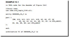
Figure 15–3 shows the circuit of Figure 15–2 reworked using a PLD to decode the addresses for the system. Notice that address bits A15–A4 are decoded by the PLD and the switch is connected to two of the PLD inputs. This change allows four different I/O port addresses for each latch, making the circuit more flexible. Table 15–2 shows the port number selected by switch 1–4 and switch 2–3. Example 15–1 shows the program for the PLD that causes the port assignments of Table 15–2.
Notice in Example 15–1 how the first term (U3) generates a logic 0 on the output to the decoder only when both switches are in their off positions for I/O port 0300H. It also generates a clock for U3 for I/O ports 304H, 308H, or 30CH, depending on the switch settings. The second term (U4) is active for ports 301H, 305H, 309H, or 30DH, depending on the switch settings. Again, refer to Table 15–2 for the complete set of port assignments for various switch settings. Since A15 is connected to the bottom of the switches, this circuit will also activate the latches for other I/O locations, because it is not decoded. I/O addresses 830XH will also generate clock sig- nals to the latch because A15 is not decoded.
Example 15–2 shows two C++ functions that transfer an integer to the 32-bit port. Either of these functions sends data to the port; the first is more efficient, but the second may be more readable. (Example 15–2(c) shows Example 15–2(b) in disassembled form.) Two parameters are passed to the function: One is the data to be sent to the port, and the other is the base port address. The base address is 0300H, 0304H, 0308H, or 030CH and must match the switch settings of Figure 15–3.
The 8-Bit ISA Bus Input Interface
To illustrate the input interface to the ISA bus, a pair of ADC804 analog-to-digital converters are interfaced to the ISA bus in Figure 15–4. The connections to the converters are made through a nine-pin DB9 connector. The task of decoding the I/O port addresses is more complex, because each converter needs a write pulse to start a conversion, a read pulse to read the digital data once they have been converted from the analog input data, and a pulse to enable the selection of the INTR output. Notice that the INTR output is connected to data bus bit position D0. When INTR is
input to the microprocessor, the rightmost bit of AL is tested to determine whether the converter is busy.
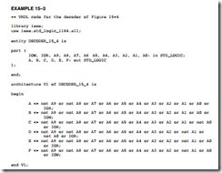
As before, great care is taken so that the connections to the ISA bus present one unit load to the system. Table 15–3 illustrates the I/O port assignment decoded by the PLD (see Example 15–3 for the program). In this example we assumed that the standard ISA bus is used, which only contains address connection A0 through A9.
Example l5–4 lists a function that can read either ADC U3 or U4. The address is generated by passing either a 0 for U3 or a 1 for U4 to the address parameter of the function. The function starts the converter by writing to it, and then waits until the INTR pin returns to a logic 0, indicating that the conversion is complete before the data are read and returned by the function as a char.
of the additional connector and its placement in the computer in relation to the 8-bit connector. Unless additional memory is added on the ISA card, the extra address connections A23–A20 do not serve any function for I/O operations. The added features that are most often used are the additional interrupt request inputs and the DMA request signals. In some systems, 16-bit I/O uses the additional eight data bus connections (D8–D15), but more often today the PCI bus is used for peripherals that are wider than 8 bits. About the only recent interfaces found for the ISA bus are a few modems and sound cards.


