8086, 80186, 80286, AND 80386SX (16-BIT) MEMORY INTERFACE
The 8086, 80186, 80286, and 80386SX microprocessors differ from the 8088/80188 in three ways:
(1) The data bus is 16 bits wide instead of 8 bits wide as on the 8088; (2) the IO>M pin of the 8088 is replaced with an M> IO pin; and (3) there is a new control signal called bus high enable (BHE). The address bit A0 or BLE is also used differently. (Because this section is based on information provided in Section 10–3, it is extremely important that you read the previous section first.) A few other differences exist between the 8086/80186 and the 80286/80386SX. The 80286/80386SX contains a 24-bit address bus (A23–A0) instead of the 20-bit address bus (A19–A0) of the 8086/80186. The 8086/80186 contain an M>IO signal, while the 80286 system and 80386SX microprocessor contain control signals MRDC and MWTC instead of RD and WR.
16-Bit Bus Control
The data bus of the 8086, 80186, 80286, and 80386SX is twice as wide as the bus for the 8088/80188. This wider data bus presents us with a unique set of problems. The 8086, 80186, 80286, and 80386SX must be able to write data to any 16-bit location—or any 8-bit location.
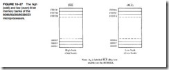
This means that the 16-bit data bus must be divided into two separate sections (or banks) that are 8 bits wide so that the microprocessor can write to either half (8-bit) or both halves (16-bit). Figure 10–27 illustrates the two banks of the memory. One bank (low bank) holds all the even- numbered memory locations, and the other bank (high bank) holds all the odd-numbered memory locations.
The 8086, 80186, 80286, and 80386SX use the BHE signal (high bank) and the A0 address bit or BLE (bus low enable) to select one or both banks of memory used for the data transfer.
Table 10–2 depicts the logic levels on these two pins and the bank or banks selected.
Bank selection is accomplished in two ways: (1) A separate write signal is developed to select a write to each bank of the memory, or (2) separate decoders are used for each bank. As a careful comparison reveals, the first technique is by far the least costly approach to memory interface for the 8086, 80186, 80286, and 80386SX microprocessors. The second technique is only used in a system that must achieve the most efficient use of the power supply.
Separate Bank Decoders. The use of separate bank decoders is often the least effective way to decode memory addresses for the 8086, 80186, 80286, and 80386SX microprocessors. This method is sometimes used, but it is difficult to understand why in most cases. One reason may be to conserve energy, because only the bank or banks selected are enabled. This is not always the case, as with the separate bank read and write signals that are discussed later.
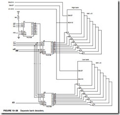
![]() Figure 10–28 illustrates two 74LS138 decoders used to select 64K RAM memory com- ponents for the 80386SX microprocessor (24-bit address). Here, decoder U2 has the BLE (A0) attached to G2A, and decoder U3 has the BHE signal attached to its G2A input. Because the decoder will not activate until all of its enable inputs are active, decoder U2 activates only for a 16-bit operation or an 8-bit operation from the low bank. Decoder U3 activates for a 16-bit operation
Figure 10–28 illustrates two 74LS138 decoders used to select 64K RAM memory com- ponents for the 80386SX microprocessor (24-bit address). Here, decoder U2 has the BLE (A0) attached to G2A, and decoder U3 has the BHE signal attached to its G2A input. Because the decoder will not activate until all of its enable inputs are active, decoder U2 activates only for a 16-bit operation or an 8-bit operation from the low bank. Decoder U3 activates for a 16-bit operation
or an 8-bit operation to the high bank. These two decoders and the sixteen 64K-byte RAMs they control represent a 1M range of the 80386SX memory system. Decoder U1 enables U2 and U3 for memory address range 000000H–0FFFFFH.
Notice in Figure 10–28 that the A0 address pin does not connect to the memory because it does not exist on the 80386SX microprocessor. Also notice that address bus bit position A1 is connected to memory address input A0, A2 is connected to A1, and so forth. The reason is that A0 from the 8086/80186 (or BLE from the 80286/80386SX) is already connected to decoder U2 and does not need to be connected again to the memory. If A0 or BLE is attached to the A0 address pin of memory, every other memory location in each bank of memory would be used. This means that half of the memory is wasted if A0 or BLE is connected to A0.
Separate Bank Write Strobes. The most effective way to handle bank selection is to develop a separate write strobe for each memory bank. This technique requires only one decoder to select a 16-bit-wide memory, which often saves money and reduces the number of components in a system.
Why not also generate separate read strobes for each memory bank? This is usually unnecessary because the 8086, 80186, 80286, and 80386SX microprocessors read only the byte of data that they need at any given time from half of the data bus. If 16-bit sections of data are always presented to the data bus during a read, the microprocessor ignores the 8-bit section that it doesn’t need, without any conflicts or special problems.
Figure 10–29 depicts the generation of separate 8086 write strobes for the memory. Here, a 74LS32 OR gate combines A0 with WR for the low bank selection signal (LWR), and BHE combines with WR for the high bank selection signal (HWR). Write strobes, for the 80286/80386SX, are generated by using the MWTC signal instead of WR.
A memory system that uses separate write strobes is constructed differently from either the 8-bit system (8088) or the system using separate memory banks. Memory in a system that uses separate write strobes is decoded as 16-bit-wide memory. For example, suppose that a memory system will contain 64K bytes of SRAM memory. This memory requires two 32K-byte memory devices (62256) so that a 16-bit-wide memory can be constructed. Because the memory is 16 bits wide and another circuit generates the bank write signals, address bit A0 becomes a don’t care. In fact, A0 is not even a pin on the 80386SX microprocessor.
Example 10–6 shows how a 16-bit-wide memory stored at locations 060000H–06FFFFH is decoded for the 80286 or 80386 microprocessor. Memory in this example is decoded, so bit A0 is a don’t care for the decoder. Bit positions A1–A15 are connected to memory component address pins A0–A14. The decoder (GAL22V10) enables both memory devices by using address connection A23–A15 to select memory whenever address 06XXXXH appears on the address bus.
Figure 10–30 illustrates this simple circuit by using a GAL22V10 to both decode memory and generate the separate write strobe. The program for the GAL22V10 decoder is illustrated in Example 10–7. Notice that not only is the memory selected, but both the lower and upper write strobes are also generated by the PLD.
Figure 10–31 depicts a small memory system for the 8086 microprocessor that contains an EPROM section and a RAM section. Here, there are four 27128 EPROMs (16K × 8) that com- pose a 32K × 16-bit memory at locations F0000–FFFFFH and four 62256 (32K × 8) RAMs that compose 64K × 16-bit memory at locations 00000H–1FFFFH. (Remember that even though the memory is 16 bits wide, it is still numbered in bytes.)
This circuit uses a 74HC139 dual 2-to-4 line decoder that selects EPROM with one half and RAM with the other half. It decodes memory that is 16 bits wide, not 8 bits, as before. Notice that the RD strobe is connected to all the EPROM OE inputs and all RAM OE input pins. This is done because even if the 8086 is reading only 8 bits of data, the application of the remaining 8 bits to the data bus has no effect on the operation of the 8086.
The LWR and HWR strobes are connected to different banks of the RAM memory. Here, it does matter whether the microprocessor is doing a 16-bit or an 8-bit write. If the 8086 writes a 16-bit number to memory, both LWR and HWR go low and enable the WE pins in both memory banks. But if the 8086 does an 8-bit write, only one of the write strobes goes low, writing to only one memory bank. Again, the only time that the banks make a difference is for a memory write operation.
Notice that an EPROM decoder signal is sent to the 8086 wait state generator because EPROM memory usually requires a wait state. The signal comes from the NAND gate used to select the EPROM decoder section, so that if EPROM is selected, a wait state is requested.
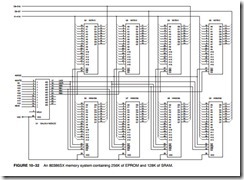
Figure 10–32 illustrates a memory system connected to the 80386SX microprocessor by using a GAL22V10 as a decoder. This interface contains 256K bytes of EPROM in the form of
four 27512 (64K × 8) EPROMs and 128K bytes of SRAM memory found in four 62256 (32K × 8) SRAMs.
Notice in Figure 10–32 that the PLD also generates the memory bank write signals LWR and HWR. As can be gleaned from this circuit, the number of components required to interface memory has been reduced to just one, in most cases (the PLD). The program listing for the PLD is located in Example 10–8. The PLD decodes the 16-bit-wide memory addresses at locations 000000H–01FFFFH for the SRAM and locations FC0000H–FFFFFFH for the EPROM.


