Operating Modes of 8253
Each of the three counters of 8253 can be operated in one of the following six modes of operation.
1. Mode0 (Interrupt on terminal count)
2. Model (Programmable monoshot)
3. Mode2 (Rate generator)
4. Mode3 (Square wave generator)
5.Mode4 (Software Triggered robe)
6.Mode5 (Hardware triggerred strobe)
In this section, we will discuss all these modes of operation of 8253 in brief.
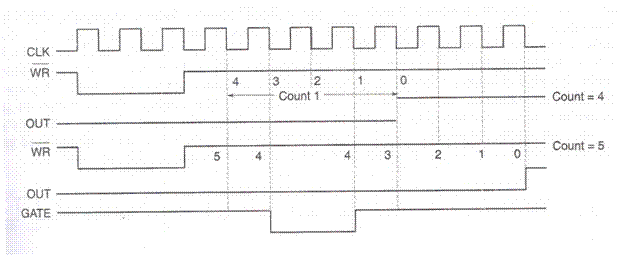
MODE 0 This mode of operation is generally called as interrupt on terminal count. In this mode, the output is initially low after the mode is set. The output remains low even after the count value is loaded in the counter. The counter starts decrementing the count value after the falling edge of the clock, if the GATE input is high. The process of decrementing the counter continues at each falling edge of the clock till the terminal count is reached, i.e. the count becomes zero. When the terminal count is reached, the output goes high and remains high till the selected control word register or the corresponding count register is reloaded with a new mode of operation or a new count, respectively. This high output may be used to interrupt the processor whenever required, by setting suitable terminal count. Writing a count register while the previous counting is in process, generates the following sequence of response.
The first byte of the new count when loaded in the count register, stops the previous count. The second byte when written, starts the new count, terminating the previous count then and there.
The GATE signal is active high and should be high for normal counting. When GATE goes low counting is terminated and the current count is latched till the GATE again goes high. Figure 1.3 shows the operational waveforms in mode0.
Fig1.3. Waveforms WR, OUT and GATE in Mode 0
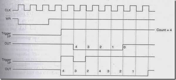
MODE 1 This mode of operation of 8253 is called as programmable one-shot mode. As the name implies, in this mode, the 8253 can be used as a monostable multivibrator. The duration of the quasistable state of the monstable multivibrator is decided by the count loaded in the count register. The gate input is used as trigger input in this mode of operation. Normally the output remains high till the suitable count is loaded in the count register and a trigger is applied. After the application of a trigger (on the positive edge), the output goes low and remains low till the count becomes zero. If another count is loaded when the output is already low, it does not disturb the previous count till a new trigger pulse is applied at the GATE input. The new counting starts after the new trigger pulse. Figure 1.4 shows the related waveforms for mode 1.
Fig1.4. WR, GATE and OUT Waveforms in Mode 1
MODE 2 This mode is called either rate generator or divide by N counter. In this mode, if N is loaded as the count value, then, after N pulses, the output becomes low only for one clock cycle. The count N is reloaded and again the output becomes high and remains high for N clock pulses. The output is normally high after initialisation or even a low signal on GATE input can force the output high. If GATE goes high, the counter starts counting down from the initial value. The counter generates an active low pulse at the output initially, after the count register is loaded with a count value. Then count down starts and whenever the count becomes zero another active low pulse is generated at the output. The duration of these active low pulses are equal to one clock cycle. The number of input clock pulses between the two low pulses at the output is equal to the count loaded. Figure 1.5 shows the related waveforms for mode 2. Interestingly, the counting is inhibited when GATE becomes low.
Fig1.5.Waveforms at pin WR and OUT in Mode 2
MODE 3 In this mode, the 8253 can be used as a square wave rate generator. In terms of operation this mode is somewhat similar to mode 2. When, the count N loaded is even, then for half of the count, the output remains high and for the remaining half it remains low. If the count loaded is odd, the first clock pulse decrements it by 1 resulting in an even count value (holding the output high). Then the output remains high for half of the new count and goes low for the remaining half. This procedure is repeated continuously resulting in the generation of a square wave. In case of odd count, the output is high for longer duration and low for shorter duration. The difference of one clock cycle duration between the two periods is due to the initial decrementing of the odd count. The waveforms for mode 3 are shown in Fig. 1.6. In general, if the loaded count value ‘N is odd, then for (N+l)/2 pulses the output remains high and for (N-l)/2 pulses it remains low.
Fig1.6.Waveforms for Mode 3
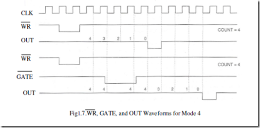
MODE 4 This mode of operation of 8253 is named as software triggerred strobe. After the mode is set, the output goes high. When a count is loaded, counting down starts. On terminal count, the output goes low for one clock cycle, and then it again goes high. This low pulse can be used as a strobe, while interfacing the microprocessor with other peripherals. The count is inhibited and the count value is latched, when the GATE signal goes low. If a new count is loaded in the count register while the previous counting is in progress, it is accepted from the next clock cycle. The counting then proceeds according to the new count. The related waveforms are shown in Fig. 1.7.
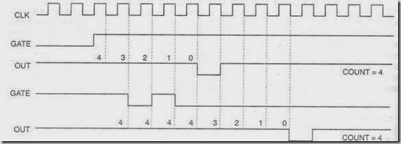
MODE 5 This mode of operation also generates a strobe in response to the rising edge at the trigger input. This mode may be used to generate a delayed strobe in response to an externally generated signal. Once this mode is programmed and the counter is loaded, the output goes high. The counter starts counting after the rising edge of the trigger input (GATE). The output goes low for one clock period, when the terminal count is reached. The output will not go low until the counter content becomes zero after the rising edge of any trigger. The GATE input in this mode is used as trigger input. The related waveforms are shown in Fig. 1.8.
Fig1.8. Waveforms in Mode 5
Programming and Interfacing 8253
As it is evident from the previous discussion, there may be two types of write operations in 8253, viz. (i) writing a control word into a control word register and (ii) writing a count value into a count register. The control word register accepts data from the data buffer and initializes the counters, as required. The control word register contents are used for (a) initialising the operating modes (mode0-mode4) (b) selection of counters (counter0-counter2) (c) choosing binary BCD counters (d) loading of the counter registers. The mode control register is a write only register and the CPU cannot read its contents.
One can directly write the mode control word for counter 2 or counter 1 prior to writing the control word for counter0. Mode control word register has a separate address, so that it can be written independently. A count register must be loaded with the count value, in the same byte sequence that was programmed in the mode control word of that counter, using the bits RL0 and RL1. The loading of the count registers of different counters is again sequence independent. One can directly write the 16-bit count register for count 2 before writing count 0 and count 1, but the two bytes in a count must be written in the byte sequence programmed using RL0 and RL1 bits of the mode control word of the counter. All the counters in 8253 are down counters, hence their count values go on decrementing if the CLK input pin is applied with a valid clock signal. A maximum count is obtained by loading all zeros into a count register, i.e.
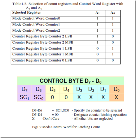
216 for binary counting and 104 for BCD counting. The 8253 responds to the negative clock edge of the clock input. The maximum operating clock frequency of 8253 is 2.6 MHz. For higher frequencies one can use timer 8254, which operates up to 10 MHz, maintaining pin compatibility with 8253. The following Table 6.2 shows the selection of different mode control words and counter register bytes depending upon address lines Ao and A1
Table 1.2 Selection of Count Registers and Control Word Register with A1 and A0. In most of the practical applications, the counter is to be read and depending on the contents of the counter a decision is to be taken. In case of 8253, the 16-bit contents of the counter can simply be read using successive 8-bit IN operations. As stated earlier, the mode control register cannot be read for any of the counters. There are two methods for reading 8253 counter registers. In the first method, either the clock or the counting procedure (using GATE) is inhibited to ensure a stable count. Then the contents are read by selecting the suitable counter using A0, Al and executing using IN instructions. The first IN instruction reads the least significant byte and the second IN instruction reads the most significant byte. Internal logic of 8253 is designed in such a way that the programmer has to complete the reading operation as programmed by him, using RL0 and RLl bits of control word.
In the second method of reading a counter, the counter can be read while counting is in progress. This method, as already mentioned is called as reading on fly. In this method, neither clock nor the counting needs to be inhibited to read the counter. The content of a counter can be read ‘on fly’ using a newly defined control word register format for online reading of the count register. Writing a suitable control word, in the mode control register internally latches the contents of the counter. The control word format for ‘read on fly’ mode is given in Fig. 1.9 along with its bit definitions. After latching the content of a counter using this method, the programmer can read it using IN instructions, as discussed before.
Example:
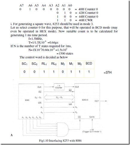
Design a programmable timer using 8253 and 8086. Interface 8253 at an address 0040H for counter 0 and write the following ALPs. The 8086 and 8253 run at 6 MHz and 1.5 MHz respectively,
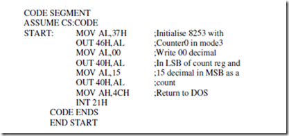
1. To generate a square wave of period 1 ms.
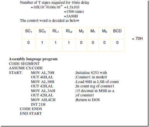
2. To interrupt the processor after 10 ms.
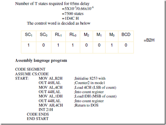
3. To derive a monoshot pulse with quasistable state duration 5 ms.
Solution: Neglecting the higher order address lines (A16-A8) the interfacing circuit diagram is shown in Fig. 1.10. The 8253 is interfaced with lower order data bus (D0-D7), hence A0 is used for selecting the even bank. The A0 and A1 of the 8253 are connected with A1 and A2 of the processor. The counter addresses can be decoded as given below. If A0 is 1, the 8253 will not be selected at all.
ii. For generating interrupt to the processor after 10ms, the 8253 is to be used in mode 0. The OUT1 pin of 8253 is connected to interrupt input of the processor. Let us use counter 1 for this purpose, and operate the 8253 in HEX count mode.
iii. For generating a 5ms quasistable state duration, the count required is calculated first. The counter 2 of 8253 is used in mode1, to count in binary. The OUT2 signal normally remains high after the count is loaded, till the trigger is applied. After the application of trigger signal, the output goes low in the next cycle, count down starts and whenever the count goes zero the output again goes high.
PROGRAMMABLE INTERRUPT CONTROLLER 8259A
The processor 8085 had five hardware interrupt pins. Out of these five interrupt pins, four pins were allotted fixed vector addresses but the pin INTR was not allotted any vector address, rather an external device was supposed to hand over the type of the interrupt, i.e. (Type 0 to 7 for RST0 to RST7), to the microprocessor. The microprocessor then gets this type and derives the interrupt vector address from that. Consider an application, where a number of I/O devices connected with a CPU desire to transfer data using interrupt driven data transfer mode. In these types of applications, more number of interrupt pins are required than available in a typical microprocessor. Moreover, in these multiple interrupt systems, the processor will have to take care of the priorities for the interrupts, simultaneously occur· ring at the interrupt request pins.
To overcome all these difficulties, we require a programmable interrupt controller which is able to handle a number of interrupts at a time. This controller takes care of a number of simultaneously appearing interrupt requests along with their types and priorities. This will relieve the processor from all these tasks. The programmable interrupt controller 8259A from Intel is one such device. The predecessor 8259 was designed to operate only with 8-bit processors like 8085. A modified version, 8259A was later introduced that is compatible with 8-bit as well as 16-bit processors.
Architecture and Signal Descriptions of 8259A
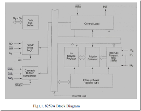
The architectural block diagram of 8259A is shown in Fig. 1.1. The functional explanation of each block is given in the following text in brief.
Interrupt Request Register (IRR) The interrupts at IRQ input lines are handled by Interrupt Request Register internally. IRR stores all the interrupt requests in it in order to serve them one by one on the priority basis.
In-Service Register (ISR) This stores all the interrupt requests those are being served, i.e ISR keeps a track of the requests being served.
Priority Resolver This unit determines the priorities of the interrupt requests appearing simultaneously. The highest priority is selected and stored into the corresponding bit of ISR during INTA pulse. The IR0 has the highest priority while the IR7 has the lowest one, normally in fixed priority mode. The priorities however may be altered by programming the 8259A in rotating priority mode.
Interrupt Mask Register (IMR) This register stores the bits required to mask the interrupt puts. IMR operates on IRR at the direction of the Priority Resolver.
Interrupt Control Logic This block manages the interrupt and interrupt acknowledge sigD8ls to be sent to the CPU for serving one of the eight interrupt requests. This also accepts interrupt acknowledge (INTA) signal from CPU that causes the 8259A to release vector address on to the data bus.
Data Bus Buffer This tristate bidirectional buffer interfaces internal 8259A bus to the microprocessor system data bus. Control words, status and vector information pass through buffer during read or write operations.
Read write Control Logic This circuit accepts and decodes commands from the CPU. This also allows the status of the 8259A to be transferred on to the data bus.
Cascade Buffer/Comparator This block stores and compares the ID’s of all the 8259As used in the system. The three I/O pins CAS0-2 are outputs
when the 8259A is used as a master. The same pins act as inputs when the 8259A is in slave mode. The 8259A in master mode sends the ID of the interrupting slave device on these lines. The slave thus selected, will send its pre programmed vector address on the data bus during the next INTA pulse.
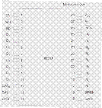
Figure 1.2 shows the pin configuration of 8259A, followed by their functional description of each of the signals in brief.
Fig.1.2. 8259 Pin Diagram
CS This is an active-low chip select signal for enabling RD* and WR* operations of 8259A.INTA* function is independent of CS*.
WR* This pin is an active-low write enable input to 8259A. This enables it to accept command words from CPU.
RD* This is an active-low read enable input to 8259A. A low on this line enables 8259A to release status onto the data bus of CPU.
D7-D0 These pins form a bidirectional data bus that carries 8-bit data either to control word or from status word registers. This also carries interrupt vector information.
CASo-CAS2 Cascade Lines A single 8259A provides eight vectored interrupts. If more interrupts are required, the 8259A is used in cascade
mode. In cascade mode, a master 8259A along with eight slaves 8259A can provide up to 64 vectored interrupt lines. These three lines act as select lines for addressing the slaves 8259A.
PS*/EN* This pin is a dual purpose pin. When the chip is used in buffered mode, it can be used as buffer enable to control buffer transreceivers. If this is not used in buffered mode then the pin is used as input to designate whether the chip is used as a master (SP = 1) or a slave (EN = 0).
INT This pin goes high whenever a valid interrupt request is asserted. This is used to interrupt the CPU and is connected to the interrupt input of CPU.
IR0-IR7(1nterrupt requests) These pins act as inputs to accept interrupt requests to the CPU. In edge triggerred mode, an interrupt service is requested by raising an IR pin from a low to a high state and holding it high until it is acknowledged, and just by latching it to high level, if used in level triggered mode.
INTA* (Interrupt acknowledge) This pin is an input used to strobe-in 8259A interrupt vector data on to the data bus. In conjunction with CS, WR, and RD pins, this selects the different operations like, writing command words, reading status word, etc.
The device 8259A can be interfaced with any CPU using either polling or interrupt. In polling, the CPU keeps on checking each peripheral device in sequence to ascertain if it requires any service from the CPU. If any such service request is noticed, the CPU serves the request and then goes on to the next device in sequence. After all the peripheral devices are scanned as above the CPU again starts from the first device. This type of system operation results in the reduction of processing speed because most of the CPU time is consumed in polling the peripheral devices.
In the interrupt driven method, the CPU performs the main processing task till it is interrupted by a service requesting peripheral device. The net processing speed of these type of systems is high because the CPU serves the peripheral only if it receives the interrupt request. If more than one interrupt requests are received at a time, all the requesting peripherals are served one by one on priority basis. This method of interfacing may require additional hardware if number of peripherals to be interfaced is more than the interrupt pins available with the CPU.
Interrupt Sequence in an 8086 System
The interrupt sequence in an 8086-8259A system is described as follows:
1. One or more IR lines are raised high that set corresponding IRR bits.
2. 8259A resolves priority and sends an INT signal to CPU.
3. The CPU acknowledges with INTA pulse.
4. Upon receiving an INTA signal from the CPU, the highest priority ISR bit is set and the corresponding IRR bit is reset. The 8259A does not drive data bus during this period.
5. The 8086 will initiate a second INTA pulse. During this period 8259A releases an 8-bit pointer on to data bus from where it is read by the CPU.
6. This completes the interrupt cycle. The ISR bit is reset at the end of the second INTA pulse if automatic end of interrupt (AEOI) mode is programmed. Otherwise ISR bit remains set until an appropriate EOI command is issued at the end of interrupt subroutine.
