Static Memory Interfacing
The general procedure of static memory interfacing with 8086 as follows:
1. Arrange the available memory chips so as to obtain 16-bit data bus width. The upper 8-bit bank is called ‘odd address memory bank’ and the lower 8-bit bank is called ‘even address memory bank’.
2. Connect available memory address lines of memory chips with those of the microprocessor and also connect the memory RD and WR inputs to the corresponding processor control signals. Connect the 16-bit data bus of the memory bank with that of the microprocessor 8086.
3. The remaining address lines of the microprocessor, BHE and Ao are used for decoding the required chip select signals for the odd and even memory banks. The CS of memory is derived from the output of the decoding circuit.
4. As a good and efficient interfacing practice, the address map of the system should be continuous as far as possible
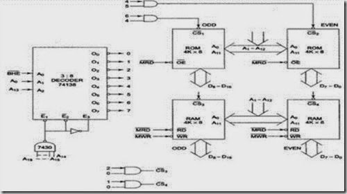
Problem 1 : Interface two 4Kx8 EPROMS and two 4Kx8 RAM chips with 8086. select suitable maps.
Solution: After reset, the IP nad CS are initialised to form address FFFFOH. Hence, this adress must lie in the EPROM. The address of RAM may be selected any where in the 1MB address space of 8086. We will select the RAM address such that the address map of the system is continuous, as shown in Table 1. Total 8K bytes of EPROM need 13 address lines Ao-A12 (since 2^13=8K). Adress lines A13 – A19 are used for decoding to generate the chip select
Fig shows the interfacing diagram for the memory system
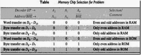
The memory system in this example contains in total four 4Kx8 memory chip. The two 4Kx8 chips of RAM and ROM are arranged in parallel to obtain 16-bit data bus width. Ao is 0, i.e. the address is even and is in RAM, then the lower RAM chip is selected indicating 8-bit transfer at an even address. If Ao is 1, i.e. the address is odd and is in RAM, the BHE goes low, the upper RAM chip is selected, further indicating that the 8-bit transfer is at an odd address. The selection of chips here takes place as shown in table 2.
Dynamic RAM Interfacing
The basic Dynamic RAM cell uses a capacitor to store the charge as a representation of data. This capacitor is manufactured as a diode that is reverse-biased so that the storage capacitance comes into the picture. This storage capacitance is utilized for storing the charge representation of data but the reverse-biased diode has a leakage current that tends to discharge the capacitor giving rise to the possibility of data loss.
To avoid this possible data loss, the data stored in a dynamic RAM cell must be refreshed after a fixed time interval reguraly. The process of refreshing the data in the RAM is known as refresh cycle. This activity is similar to reading the data from each cell of the memory, independent of the requirement of microprocessor, regularly. During this refresh period all other operations (accesses) related to the memory subsystem are suspended.
The advantages of dynamic RAM. Like low power consumption, higher packaging density and low cost, most of the advanced computer systems are designed using dynamic RAMs. Also the refresh mechanism and the additional hardware required makes the interfacing hardware, in case of dynamic RAM, more complicated, as compared to static RAM interfacing circuit.
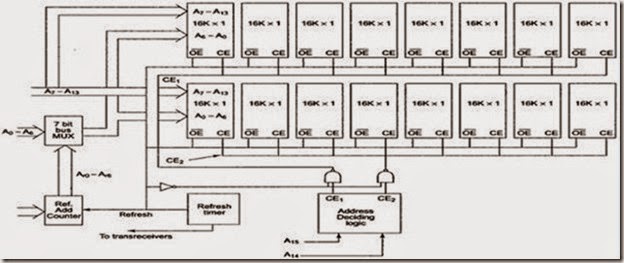
Generally dynamic RAM is available in units of several Kilobits to even Megabits of memory (note that it is not in terms bytes or nibbles as in a static RAM). This memory is arranged internally in a two dimensional matrix array so that it will have n rows and m columns. The diagram shown in figure explains the refreshing logic and 8086 interfacing with dynamic RAM.
Each of the used chips 16K * 1-bit Dynamic RAM cell array. The system contains two 16 Kbytes Dynamic RAM units. All the address and the data lines are assumed to be available from an 8086 microprocessor system. The OE pin controls output data buffers of the memory chip.
The CE pins are active high chip select of memory chips. The refresh cycle starts, if the refresh output of the refresh timer goes high. The high CE enables the memory chip for refreshing .
Interfacing I/O Ports
I/O ports or input/output ports are the devices through which the microprocessor communicates with other devices or external data sources/destinations. Input activity, as one may expect, is the activity that enables the microprocessor to read data from external devices, for example keyboard, joysticks, mouser etc. the devices are known as input devices as they feed data into a microprocessor system.
Output activity transfers data from the microprocessor top the external devices, for example CRT display, 7-segment displays, printer, etc, the devices that accept the data from a microprocessor system are called output devices.
Steps in Interfacing an I/O Device
The following steps are performed to interface a general I/O device with a CPU:
1. Connect the data bus of the microprocessor system with the data bus of the I/O port.
2. Derive a device address pulse by decoding the required address of the device and use it as the chip select of the device.
3. Use a suitable control signal, i.e. IORD and /or IOWR to carry out device operations, i.e. connect IORD to RD input of the device if it is an input devise, otherwise connect IOWR to WR input of the device. In some cases the RD or WR control signals are combined with the device address pulse to generate the device select pulse.
Input Port
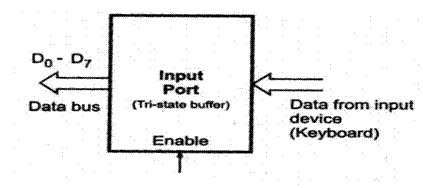
The input device is connected to the microprocessor through buffer. The simplest form of a input port is a buffer as shown in the figure.
This buffer is a tri-state buffer and its output is available only when enable signal is active. When microprocessor wants to read data from the input device (keyboard), the control signals from the microprocessor activates the buffer by asserting enable input of the buffer. Once the buffer is enabled, data from the device is available on the data bus. Microprocessor reads this data by initiating read command.
Output Port
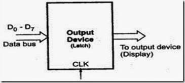
It is used to send the data to the output device such as display from the microprocessor. The simplest form of the output port is a latch.
The output device is connected to the microprocessor through latch as shown in the figure. When microprocessor wants to send data to the output device it puts the data on the data bus and activates the clock signal of the latch, latching the data from the data bus at the output of latch. It is then available at the output of latch for the output device.
I/O Interfacing Techniques
Input/output devices can be interfaced with microprocessor systems in two ways :
1. I/O mapped I/O
2. Memory mapped I/O
1. I/O mapped I/O :
8086 has special instructions IN and OUT to transfer data through the input/output ports in I/O mapped I/O system. The IN instruction copies data from a port to the Accumulator. If an 8-bit port is read data will go to AL and if 16-bit port is read the data will go to AX.
The OUT instruction copies a byte from AL or a word from AX to the specified port. The M/IO signal is always low when 8086 is executing these instructions. In this address
of I/O device is 8-bit or 16-bit. It is 8-bit for Direct addressing and 16-bit for Indirect addressing.
2. Memory mapped I/O
In this type of I/O interfacing, the 8086 uses 20 address lines to identify an I/O device. The I/O device is connected as if it is a memory device. The 8086 uses same control signals and instructions to access I/O as those of memory, here RD and WR signals are activated indicating memory bus cycle.
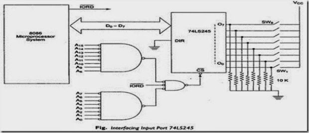
Problem : Interface an input port 74LS245 to read the status of the switches SW1 to SW8. the switches when shorted, input a ‘1’ else input a ‘0’ to the microprocessor system. Store the status in register BL. The address of the port is 0740H
Solution :
The hardware interface circuit is shown in figure. The address, control and data lines are assumed to be readily available at the microprocessor system The ALP is given as follows :
|
MOV BL, 00H |
; |
|
clear BL for status |
|
MOV DX, 0740H |
|
; |
16-bit Port address in DX |
|
IN AL,DX |
; |
|
Read Port 0740H for switch positions. |
|
MOV BL,AL |
; |
|
Store status of switches from AL into BL |
|
HLT |
; |
|
Stop |
Problem :
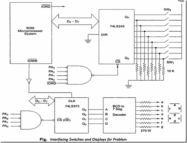
Design an interface of input port 74LS245 to read the status of switches SW1 to SW8 and output port 74LS373 with 8086. display the number of key that is pressed with the help of output port on 7 segment display.
Solution : Status of the switches is first read into the AL. Displaying the shorted switch number in the 7 segment display. Instead of using 16 address lines, one may use only A3
– A0.

