Signal Description of 8086 Microprocessor
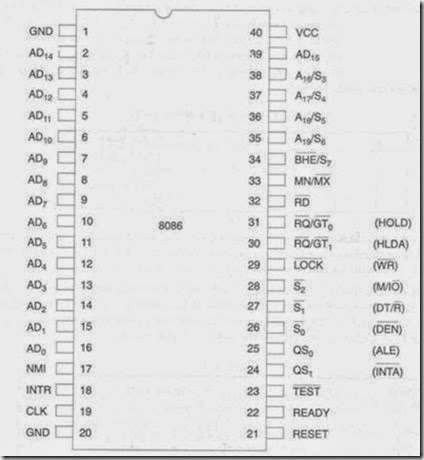
The 8086 Microprocessor is a 16-bit CPU available in 3 clock rates, i.e. 5, 8 and 10MHz, packaged in a 40 pin CERDIP or plastic package. The 8086 Microprocessor operates in single processor or multiprocessor configurations to achieve high performance. The pin configuration is as shown in fig1. Some of the pins serve a particular function in minimum mode (single processor mode) and others function in maximum mode (multiprocessor mode) configuration.
Maximum mode
The 8086 signals can be categorized in three groups. The first are the signals having common functions in minimum as well as maximum mode, the second are the signals which have special functions in minimum mode and third are the signals having special functions for maximum mode
The following signal description are common for both the minimum and maximum modes.
![]() AD15-AD0: These are the time multiplexed memory I/O address and data lines. Address remains on the lines during T1 state, while the data is available on the data bus during T2, T3, TW and T4. Here T1, T2, T3, T4 and TW are the clock states of a machine cycle. TW is a wait state. These lines are active high and float to a tristate during interrupt acknowledge and local bus hold acknowledge cycles.
AD15-AD0: These are the time multiplexed memory I/O address and data lines. Address remains on the lines during T1 state, while the data is available on the data bus during T2, T3, TW and T4. Here T1, T2, T3, T4 and TW are the clock states of a machine cycle. TW is a wait state. These lines are active high and float to a tristate during interrupt acknowledge and local bus hold acknowledge cycles.
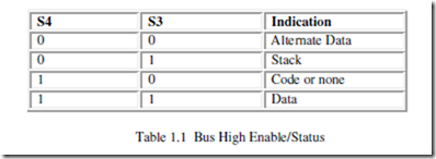
A19/S6, A18/S5, A17/S4, A16/S3: These are the time multiplexed address and status lines. During T1, these are the most significant address lines or memory operations. During I/O operations, these lines are low. During memory or I/O operations, status information is available on those lines for T2, T3, TW and T4 .The status of the interrupt enable flag bit(displayed on S5) is updated at the beginning of each clock cycle. The S4 and S3 combinedly indicate which segment register is presently being used for memory accesses as shown in Table 1.1.
These lines float to tri-state off (tristated) during the local bus hold acknowledge. The status line S6 is always low(logical). The address bits are separated from the status bits using latches controlled by the ALE signal.
BHE/S7–Bus High Enable/Status: The bus high enable signal is used to indicate the transfer of data over the higher order (D15-D8) data bus as shown in Table 1.2. It goes low for the data transfers over D15-D8 and is used to derive chip selects of odd address memory bank or peripherals. BHE is low during T1 for read, write and interrupt acknowledge cycles, when- ever a byte is to be transferred on the higher byte of the data bus. The status information is available during T2, T3 and T4. The signal is active low and is tristated during ‘hold’. It is low during T1 for the first pulse of the interrupt acknowledge cycle.
![]() RD-Read: Read signal, when low, indicates the peripherals that the processor is performing a memory or I/O read operation. RD is active low and shows the state for T2, T3, TW of any read cycle. The signal remains tristated during the ‘hold acknowledge’.
RD-Read: Read signal, when low, indicates the peripherals that the processor is performing a memory or I/O read operation. RD is active low and shows the state for T2, T3, TW of any read cycle. The signal remains tristated during the ‘hold acknowledge’.
READY: This is the acknowledgement from the slow devices or memory that they have completed the data transfer. The signal made available by the devices is synchronized by the 8284A clock generator to provide ready input to the 8086. The signal is active high.
INTR-lnterrupt Request: This is a level triggered input. This is sampled during the last clock cycle of each instruction to determine the availability of the request. If any interrupt request is pending, the processor enters the interrupt acknowledge cycle. This can be internally masked by resetting the interrupt enable flag. This signal is active high and internally synchronized.
TEST: This input is examined by a ‘WAIT’ instruction. If the TEST input goes low, execution will continue, else, the processor remains in an idle state. The input is synchronized internally during each clock cycle on leading edge of clock.
NMI-Non-maskable Interrupt: This is an edge-triggered input which causes a Type2 interrrupt. The NMI is not maskable internally by software. A transition from low to high initiates the interrupt response at the end of the current instruction. This input is internally synchronized.
RESET: This input causes the processor to terminate the current activity and start execution from FFFF0H. The signal is active high and must be active for at least four clock cycles. It restarts execution when the RESET returns low. RESET is also internally synchronized.
CLK-Clock Input: The clock input provides the basic timing for processor operation and bus control activity. Its an asymmetric square wave with 33% duty cycle. The range of frequency for different 8086 versions is from 5MHz to 10MHz.
VCC : +5V power supply for the operation of the internal circuit. GND ground for the internal circuit.
MN/MX :The logic level at this pin decides whether the processor is to operate in either minimum (single processor) or maximum (multiprocessor) mode.
The following pin functions are for the minimum mode operation of 8086.
M/IO -Memory/IO: This is a status line logically equivalent to S2 in maximum mode. When it is low, it indicates the CPU is having an I/O operation, and when it is high, it indicates that the CPU is having a memory operation. This line becomes active in the
previous T4 and remains active till final T4 of the current cycle. It is tristated during local bus "hold acknowledge".
INTA -Interrupt Acknowledge: This signal is used as a read strobe for interrupt acknowledge cycles. In other words, when it goes low, it means that the processor has accepted the interrupt. It is active low during T2, T3 and TW of each interrupt acknowledge cycle.
ALE-Address latch Enable: This output signal indicates the availability of the valid address on the address/data lines, and is connected to latch enable input of latches. This signal is active high and is never tristated.
DT /R -Data Transmit/Receive: This output is used to decide the direction of data flow through the transreceivers (bidirectional buffers). When the processor sends out data, this signal is high and when the processor is receiving data, this signal is low. Logically, this is equivalent to S1 in maximum mode. Its timing is the same as M/I/O. This is tristated during ‘hold acknowledge’.
DEN-Data Enable This signal indicates the availability of valid data over the address/data lines. It is used to enable the transreceivers (bidirectional buffers) to separate the data from the multiplexed address/data signal. It is active from the middle ofT2 until the middle of T4 DEN is tristated during ‘hold acknowledge’ cycle.
HOLD, HLDA-Hold/Hold Acknowledge: When the HOLD line goes high, it indicates to the processor that another master is requesting the bus access. The processor, after receiving the HOLD request, issues the hold acknowledge signal on HLDA pin, in the middle of the next clock cycle after completing the current bus (instruction) cycle. At the same time, the processor floats the local bus and control lines. When the processor detects the HOLD line low, it lowers the HLDA signal. HOLD is an asynchronous input, and it should be externally synchronized.
If the DMA request is made while the CPU is performing a memory or I/O cycle, it will release the local bus during T 4 provided:
1. The request occurs on or before T 2 state of the current cycle.
2. The current cycle is not operating over the lower byte of a word (or operating on an odd address).
3. The current cycle is not the first acknowledge of an interrupt acknowledge sequence.
4. A Lock instruction is not being executed.
So far we have presented the pin descriptions of 8086 in minimum mode.
The following pin functions are applicable for maximum mode operation of 8086.
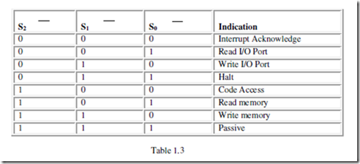
S2, S1, S0 –Status Lines: These are the status lines which reflect the type of operation, being carried out by the processor. These become active during T4 of the previous cycle
and remain active during T1 and T2 of the current bus cycle. The status lines return to passive state during T3 of the current bus cycle so that they may again become active for the next bus cycle during T4. Any change in these lines during T3 indicates the starting of a new cycle, and return to passive state indicates end of the bus cycle. These status lines are encoded in table 1.3.
LOCK: This output pin indicates that other system bus masters will be prevented from gaining the system bus, while the LOCK signal is low. The LOCK signal is activated by the ‘LOCK’ prefix instruction and remains active until the completion of the next instruction. This floats to tri-state off during "hold acknowledge". When the CPU is executing a critical instruction which requires the system bus, the LOCK prefix instruction ensures that other processors connected in the system will not gain the control of the bus. The 8086, while executing the prefixed instruction, asserts the bus lock signal output, which may be connected to an external bus controller.
QS1, QS0–Queue Status: These lines give information about the status of the code- prefetch queue. These are active during the CLK cycle after which the queue operation is performed. These are encoded as shown in Table 1.4.
This modification in a simple fetch and execute architecture of a conventional microprocessor offers an added advantage of pipelined processing of the instructions. The 8086 architecture has a 6-byte instruction prefetch queue. Thus even the largest (6- bytes) instruction can be prefetched from the memory and stored in the prefetch queue. This results in a faster execution of the instructions. In 8085, an instruction (opcode and operand) is fetched, decoded and executed and only after the execution of this instruction, the next one is fetched. By prefetching the instruction, there is a considerable speeding up in instruction execution in 8086. This scheme is known as instruction pipelining. At the starting the CS:IP is loaded with the required address from which the execution is to be started. Initially, the queue will be empty and the microprocessor starts a fetch operation to bring one byte (the first byte) of instruction code, if the CS:IP address is odd or two bytes at a time, if the CS:IP address is even. The first byte is a complete opcode in case of some instructions (one byte opcode instruction) and it is a part of opcode, in case of other instructions (two byte long opcode instructions), the remaining part of opcode may lie in the second byte. But invariably the first byte of an instruction is an opcode. These opcodes along with data are fetched and arranged in the queue. When the first byte from the queue goes for decoding and interpretation, one byte in the queue becomes empty and subsequently the queue is updated. The microprocessor does not perform the next fetch operation till at least two bytes of the instruction queue are emptied. The instruction execution cycle is never broken for fetch operation. After decoding the first byte, the decoding circuit decides whether the instruction is of single opcode byte or double opcode byte. If it is single opcode byte, the next bytes are treated as data bytes depending upon the decoded instruction length, other wise, the next byte in the queue is treated as the second byte of the instruction opcode. The second byte is then decoded in continuation with the first byte to decide the instruction length and the number of subsequent bytes to be treated as instruction data. The queue is updated after every byte is read from the queue but the fetch cycle is initiated by BIU only if at least, two bytes of the queue are empty and the EU may be concurrently executing the fetched instructions.
The next byte after the instruction is completed is again the first opcode byte of the next instruction. A similar procedure is repeated till the complete execution of the program. The main point to be noted here is, that the fetch operation of the next instruction is overlapped with the execution of the current instruction. As shown in the architecture, there are two separate units, namely, execution unit and bus interface unit. While the execution unit is busy in executing an instruction, after it is completely decoded, the bus interface unit may be fetching the bytes o( the next instruction from memory, depending upon the queue status. Figure 1.6 explains the queue operation.
RQ/GT0, RQ/GT1-ReQuest/Grant: These pins are used by other local bus masters, in maximum mode, to force the processor to release the local bus at the end of the processor’s current bus cycle. Each of the pins is bidirectional with RQ/GT0 having higher priority than RQ/ GT1, RQ/GT pins have internal pull-up resistors and may be left unconnected. The request! grant sequence is as follows:
1. A pulse one clock wide from another bus master requests the bus access to 8086.
2. During T4 (current) or T1 (next) clock cycle, a pulse one clock wide from 8086 to the requesting master, indicates that the 8086 has allowed the local bus to float and that it will enter the "hold acknowledge" state at next clock cycle. The CPU’s bus interface unit is likely to be disconnected from the local bus of the system.
3. A one clock wide pulse from the another master indicates to 8086 that the ‘hold’ request is about to end and the 8086 may regain control of the local bus at the next clock cycle.
Thus each master to master exchange of the local bus is a sequence of 3 pulses. There must be at least one dead clock cycle after each bus exchange. The request and grant pulses are active low. For the bus requests those are received while 8086 is performing memory or I/O cycle, the granting of the bus is governed by the rules as discussed i~ case of HOLD, and HLDA in minimum mode.
Until now, we have described the architecture and pin configuration of 8086. In the next section, we will study some operational features of 8086 based systems.
8284A Clock Generator
The 8284A is an ancillary component to the 8086/8088 microprocessor. Without
the clock generator, many additional circuits to generate the clock (CLK in an 8086/8088 based system. The clock Generator 8284A provides the following basic functions or signals: clock generation, RESEST synchronization, READY synchronization, and a TTL level peripheral clock signal.
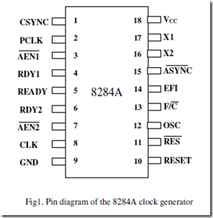
Pin Functions: The 8284A is an 18-pin integrated circuit designed specifically for use with the 8086/8088 microprocessors as shown in fig1. The following is a list of each pin and its function.
AEN1* and AEN2*: The address enable pins are provided to qualify the ready signals. RDY1 and RDY2, respectively. Which are used to cause wait states, along with the RDY1 and RDY2 inputs. Wait states are generated by the READY pin of the 8086/8088 microprocessor. This is controlled by these two inputs.
RDY1 and RDY2: The bus ready inputs are provided in conjunction with the AEN1* and AEN2* pins to cause wait states in an 8086/8088 microprocessor based system.
ASYNC*: The ready synchronization selection input selects either one or two stages of synchronization for the RDY1 and RDY2 inputs.
READY: Ready is an output pin that connects to the 8086/8088 microprocessor READY input. This signal is synchronized with the RDY1 and RDY2 inputs.
X1 and X2: The Crystal Oscillator pins connect to an external crystal used as the timing source for the clock generator and all its functions.
F/C*: The Frequency/Crystal select input results the clocking source for the 8284A. If this pin is held high, an external clock is provided to the EFI input pin, and if it is held low, the internal crystal oscillator provides the timing signal.
EFI: The External Frequency input is used when the F/C is pulled high. EFI supplies the timing whenever the F/C* pin is high.
CLK: The clock output pin provides CLK input signal to the 8086/8088 microprocessors and other components in the system. The CLK pin has an output signal that is one-third of the crystal or EFI input frequency and has a 33 percent duty cycle, which is required by the 8086/8088 microprocessors.
PCLK: The Peripheral Clock signal is one-sixth the crystal or EFI input frequency and has a 50 percent duty cycle. The PCLK output provides a clock signal to the peripheral equipment in the system.
OSC: The Oscillator output is a TTL level signal that is at the same frequency as the crystal or EFI input. (The OSC output provides and EFI input to other 8284A clock generators in some multiple processor systems).
RES*: The reset input is an active-low input to the 8284A. The RES* pin is often connected an RC network that provides power-on resetting.
RESET: The Reset output is connected to the 8086/8088 microprocessors RESET input pin.
CSYNC: The clock synchronization pin is used whenever the EFI input provides synchronization in systems with multiple processors. When the internal crystal oscillator is used, this pin must be grounded.
GND: The ground pin is connects to ground.
Vcc: This power supply pin connects to + 5.0V with a tolerance of ± 10 percent
Operation of the 8084A:
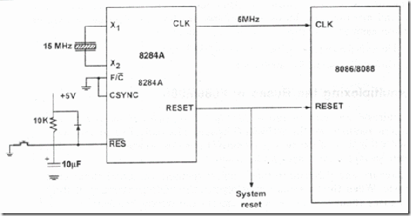
Fig1.1. The clock generator (8284A) and the 8086/8088 microprocessor illustrating the connection for the clock and reset signal. (A 15 MHz of crystal provides the 5MHz clock for the microprocessor.)
The Reset section of the 8284A is very simple. It consists of a Schmitt trigger buffer and a single D-type flip flop circuit. The D-type flip flop ensures that the timing requirements of the 8086/8088 microprocessor RESET input are met. The circuit applies the RESET signal to the microprocessor negative edge (1-to-0 transition) of each clock. The 8086/8088 microprocessor sample RESET at the positive edge (0-to-1 transition) of the clocks; therefore, the circuit meets the timing requirements of the 8086/8088 microprocessor.
The RC circuit provides a logic 0 to the RES* input pin when power is first applied to the system. After a short time, the RES* input becomes a logic 1 because the capacitor charges toward +5.0V through the resistor. A push-button switch allows the microprocessor to be reset by the operator. Correct reset timing requires the RESET input
to become logic 1 no later than four clocks after system power is applied and to be held high for at least 50µs. The flop-flop makes certain that RESET goes high in four clocks, and the RC time constant ensures that it stays high for at least 50µs.
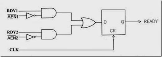
Ready Logic
The Ready Logic generates the Ready signal for the 8086/8088 microprocessor. If the Ready signal is made low by this circuit during T2 state of a machine cycle, the microprocessor introduces a wait state between T3 and T4 states of the machine cycle. The Ready logic is indicated in the figure. There are two pairs of signals in 8284 which can make the Ready output of 8284 to go low. If (RDY1=0 or AEN1*=1) and (RDY2=0 or AEN2*=1), the Ready output becomes low when the next clock transition takes place. In PCs, RDY2 and AEN2* are not used, and as such RDY2 is tied to Ground and /or AEN2* is tied to +5V. AEN1* is used for generating wait states in the 8086/8088 bus cycle, and RDY1 is used for generating wait state in the DMA bus cycle.
Reset Logic
The Reset logic generates the Reset input signal for the 8086/8088. When the RESET* pin goes low, the Reset output is generated by the 8284 when the next clock transition takes place.
In PCs, the RES* input is activated by one of the following.
-
From the manual Reset button on the front panel.
-
From the ‘Power on Reset’ circuit, which uses RC components.
-
If the ‘Power Good’ signal from the SMPS is not active.
