MINIMUM MODE 8086 SYSTEM AND TIMINGS
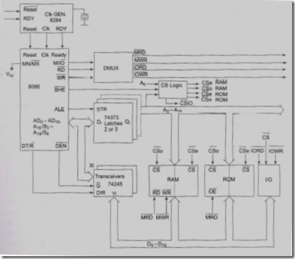
In a minimum mode 8086 system, the microprocessor 8086 is operated in minimum mode by strapping its MN/MX* pin to logic1. In this mode, all the control signals are given out by the microprocessor chip itself. There is a single microprocessor in the minimum mode system. The remaining components in the system are latches, transreceivers, clock generator, memory and I/O devices. Some type of chip selection logic may be required for selecting memory or I/O devices, depending upon the address map of the system.
The latches are generally buffered output D-type flip-flops, like, 74LS373 or 8282. They are used for separating the valid address from the multiplexed address/data signals and are controlled by the ALE signal generated by 8086. Transreceivers are the bidirectional buffers and some times they are called as data amplifiers. They are required to separate the valid data from the time multiplexed address/data signal. They are controlled by two signals, namely, DEN* and DT/R*. The DEN* signal indicates that the valid data is available on the data bus, while DT/R indicates the direction of data, i.e. from or to the processor. The system contains memory for the monitor and users program storage. Usually, EPROMS are used for monitor storage, while RAMs for users program storage. A system may contain I/O devices for communication with the processor as well as some special purpose I/O devices. The clock generator generates the clock from the crystal oscillator and then shapes it and divides to make it more precise so that it can be used as an accurate timing reference for the system. The clock generator also synchronizes some external signals with the system clock. The general system organization is shown in Fig. 1.1. Since it has 20 address lines and 16 data lines, the 8086 CPU requires three octal address latches and two octal data buffers for the complete address and data separation.
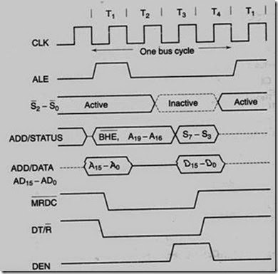
The working of the minimum mode configuration system can be better described in terms of the timing diagrams rather than qualitatively describing the operations. The opcode fetch and read cycles are similar. Hence the timing diagram can be categorized in two parts, the first is the timing diagram for read cycle and the second is the timing diagram for write cycle.
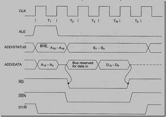
Fig 1.2 shows the read cycle timing diagram. The read cycle begins in T1 with the assertion of the address latch enable (ALE) signal and also M/IO* signal. During the negative going edge of this signal, the valid address is latched on the local bus. The BHE* and A0 signals address low, high or both bytes. From Tl to T4, the M/IO* signal indicates a memory or I/O operation. At T2 the address is removed from the local bus and is sent to the output. The bus is then tristated. The read (RD*) control signal is also activated in T2 .The read (RD) signal causes the addressed device to enable its data bus drivers. After RD* goes low, the valid data is available on the data bus. The addressed
device will drive the READY line high, when the processor returns the read signal to high level, the addressed device will again tristate its bus drivers.
Fig 1.1. Minimum Mode 8086 System
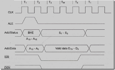
Fig 1.3 shows the write cycle timing diagram. A write cycle also begins with the assertion of ALE and the emission of the address. The M/IO* signal is again asserted to indicate a memory or I/O operation. In T2 after sending the address in Tl the processor sends the data to be written to the addressed location. The data remains on the bus until middle of T4 state. The WR* becomes active at the beginning ofT2 (unlike RD* is somewhat delayed in T2 to provide time for floating).
The BHE* and A0 signals are used to select the proper byte or bytes of memory or I/O word to be read or written. The M/IO*, RD* and WR* signals indicate the types of data transfer as specified in Table
Fig.1.2. Read Cycle Timing Diagram for Minimum Mode
HOLD Response Sequence
Fig 1.4. Bus Request and Bus Grant Timings in Minimum Mode System
The HOLD pin is checked at the end of the each bus cycle. If it is received active by the processor before T4 of the previous cycle or during T1 state of the current cycle, the CPU activities HLDA in the next clock cycle and for the succeeding bus cycles, the bus will be given to another requesting master The control control of the bus is not regained by the processor until the requesting master does not drop the HOLD pin low. When the request is dropped by the requesting master, the HLDA is dropped by the processor at the trailing edge of the next clock as shown in fig 1.4.
MAXIMUM MODE 8086 SYSTEM AND TIMINGS
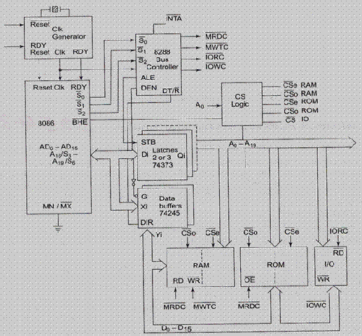
In the maximum mode, the 8086 is operated by strapping the MN/MX* pin to ground. In this mode, the processor derives the status signals S2*, S1* and S0*. Another chip called bus controller derives the control signals using this status information. In the maximum mode, there may be more than one microprocessor in the system configuration. The other components in the system are the same as in the minimum mode system. The general system organization is as shown in the fig1.1
The basic functions of the bus controller chip IC8288, is to derive control signals like RD* and WR* (for memory and I/O devices), DEN*, DT/R*, ALE, etc. using the information made available by the processor on the status lines. The bus controller chip has input lines S2*, S1* and S0* and CLK. These inputs to 8288 are driven by the CPU. It derives the outputs ALE, DEN*, DT/R*, MWTC*, AMWC*, IORC*, IOWC* and AIOWC*. The AEN*, IOB and CEN pins are specially useful for multiprocessor systems. AEN* and IOB are generally grounded. CEN pin is usually tied to +5V.
Fig 1.1 Maximum Mode 8086 System
The significance of the MCE/PDEN* output depends upon the status of the IOB pin. If IOB is grounded, it acts as master cascade enable to control cascaded 8259A; else it acts as peripheral data enable used in the multiple bus configurations. INTA* pin is used to issue two interrupt acknowledge pulses to the interrupt controller or to an interrupting device.
IORC*, IOWC* are I/O read command and I/O write command signals respectively. These signals enable an IO interface to read or write the data from or to the addressed port. The MRDC*, MWTC* are memory read command and memory write command signals respectively and may be used as memory read and write signals. All these command signals instruct the memory to accept or send data from or to the bus. For both of these write command signals, the advanced signals namely AIOWC* and AMWTC* are available. They also serve the same purpose, but are activated one clock cycle earlier than the IOWC* and MWTC* signals, respectively. The maximum mode system is shown in fig. 1.1.
The maximum mode system timing diagrams are also divided in two portions as read (input) and write (output) timing diagrams. The address/data and address/status timings are similar to the minimum mode. ALE is asserted in T1, just like minimum mode. The only difference lies in the status signals used and the available control and advanced command signals. The fig. 1.2 shows the maximum mode timings for the read operation while the fig. 1.3 shows the same for the write operation.
Fig. 1.2 Memory Read Timing in Maximum Mode
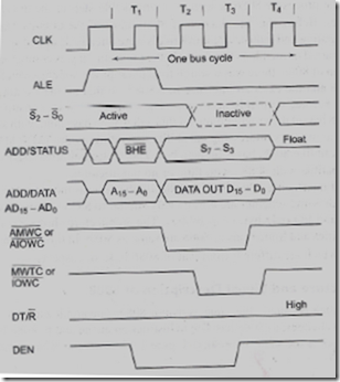 Timings for R Fig. 1.3 Memory Write Timing in Maximum Mode
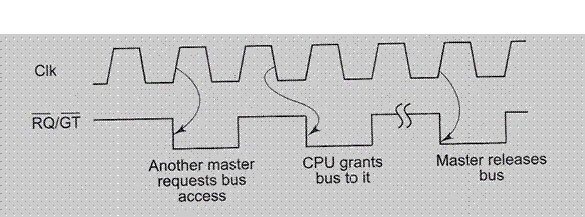 Fig1.4. RQ*/GT* Timings in Maximum Mode
