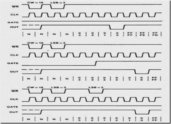
• MODE 4: SOFTWARE TRIGGERED STROBE :
• OUT will be initially high. When the initial count expires, OUT will go low for one CLK pulse and then go high again. The counting sequence is “triggered’‘ by writing the initial count.
• GATE = 1 enables counting; GATE = 0 disables counting. GATE has no effect on OUT. After writing a Control Word and initial count, the Counter will be loaded on the next CLK pulse.
• This CLK pulse does not decrement the count, so for an initial count of N, OUT does not strobe low until N + 1 CLK pulses after the initial count is written.
• If a new count is written during counting, it will be loaded on the next CLK pulse and counting will continue from the new count. If a two-byte count is written, the following happens:
1) Writing the first byte has no effect on counting.
2) Writing the second byte allows the new count to be loaded on the next CLK pulse.
• This allows the sequence to be “retriggered” by software. OUT strobes low N a 1 CLK pulses after the new count of N is written.
Figure 19. Mode 4
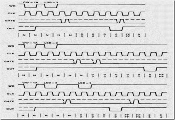
• MODE 5: HARDWARE TRIGGERED STROBE (RETRIGGERABLE):
OUT will initially be high. Counting is triggered by a rising edge of GATE. When the initial count has expired, OUT will go low for one CLK pulse and then go high again.
• After writing the Control Word and initial count, the counter will not be loaded until the CLK pulse after a trigger. This CLK pulse does not decrement the count, so for an initial count of N, OUT does not strobe low until N = 1 CLK pulses after a trigger.
• A trigger results in the Counter being loaded with the initial count on the next CLK pulse. The counting sequence is retriggerable. OUT will not strobe low for N a 1 CLK pulses after any trigger. GATE has no effect on OUT.
• If a new count is written during counting, the current counting sequence will not be affected. If a trigger occurs after the new count is written but before the current count expires, the Counter will be loaded with the new count on the next CLK pulse and counting will continue from there.
Figure 20. Mode 5
• Operation Common to All Modes:
• PROGRAMMING: When a Control Word is written to a Counter, all Control Logic is immediately reset and OUT goes to a known initial state; no CLK pulses are required for this.
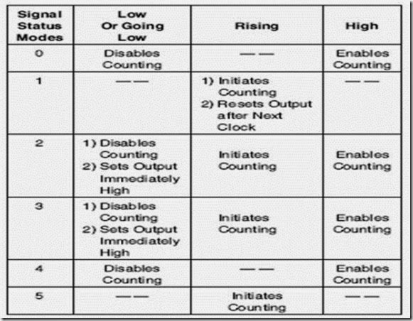
• GATE: The GATE input is always sampled on the rising edge of CLK. In Modes 0, 2, 3, and 4 the GATE input is level sensitive, and the logic level is sampled on the rising edge of CLK. In Modes 1, 2, 3, and 5 the GATE input is rising-edge sensitive.
• In these Modes, a rising edge of GATE (trigger) sets an edge-sensitive flip-flop in the Counter. This flip-flop is then sampled on the next rising edge of CLK; the flip-flop is reset immediately after it is sampled. In this way, a trigger will be detected no matter when it occurs-a high logic level does not have to be maintained until the next rising edge of CLK.
• Note that in Modes 2 and 3, the GATE input is both edge- and level-sensitive. In Modes 2 and 3, if a CLK source other than the system clock is used, GATE should be pulsed immediately following WR of a new count value.
Figure 21. Gate Pin Operations Summary
• COUNTER: New counts are loaded and Counters are decremented on the falling edge of CLK.
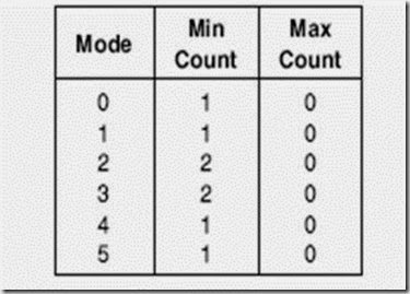
• The largest possible initial count is 0, this is equivalent to 216 for binary counting and 104 for BCD counting. The Counter does not stop when it reaches zero.
• In Modes 0, 1, 4, and 5 the Counter “wraps around” to the highest count, either FFFF hex for binary counting or 9999 for BCD counting, and continues counting.
• Modes 2 and 3 are periodic; the Counter reloads itself with the initial count and continues counting from there.
NOTE: 0 is equivalent to 216 for binary counting and 104 for BCD counting.
Figure 22. Minimum and Maximum Initial Counts
8279
• While studying 8255, we have explained the use of 8255 in interfacing keyboards and displays with 8086. The disadvantages of this method of interfacing keyboard and display with 8086 is that the processor has to refresh the display and check the status of the keyboard periodically using polling technique. Thus a considerable amount of CPU time is wasted, reducing the system operating speed.
• Intel’s 8279 is a general purpose keyboard display controller that simultaneously drives the display of a system and interfaces a keyboard with the CPU, leaving it free for its routine task.
Architecture and Signal Descriptions of 8279
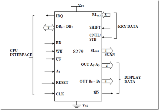
• The keyboard display controller chip 8279 provides:
a) a set of four scan lines and eight return lines for interfacing keyboards
b) A set of eight output lines for interfacing display.
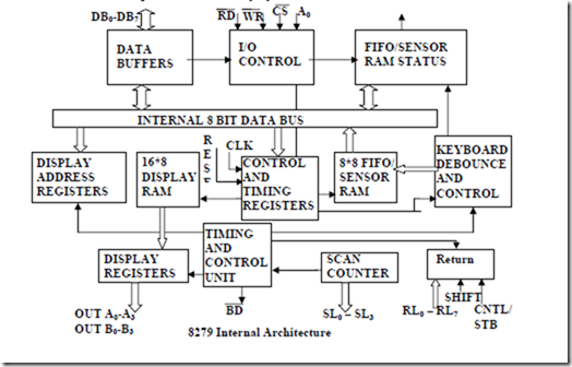
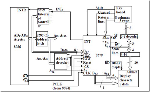
• Fig shows the functional block diagram of 8279 followed by its brief description.
• I/O Control and Data Buffers : The I/O control section controls the flow of data to/from the 8279. The data buffers interface the external bus of the system with internal bus of 8279.
• The I/O section is enabled only if CS is low. The pins A0, RD and WR select the command, status or data read/write operations carried out by the CPU with 8279.
• Control and Timing Register and Timing Control : These registers store the keyboard and display modes and other operating conditions programmed by CPU. The registers are written with A0=1 and WR=0. The Timing and control unit controls the basic timings for the operation of the circuit. Scan counter divide down the operating frequency of 8279 to derive scan keyboard and scan display frequencies.
• Scan Counter : The scan counter has two modes to scan the key matrix and refresh the display. In the encoded mode, the counter provides binary count that is to be externally decoded to provide the scan lines for keyboard and display (Four
externally decoded scan lines may drive upto 16 displays). In the decode scan mode, the counter internally decodes the least significant 2 bits and provides a decoded 1 out of 4 scan on SL0-SL3(Four internally decoded scan lines may drive upto 4 displays). The keyboard and display both are in the same mode at a time.
• Return Buffers and Keyboard Debounce and Control: This section for a key closure row wise. If a key closer is detected, the keyboard debounce unit debounces the key entry (i.e. wait for 10 ms). After the debounce period, if the key continues to be detected. The code of key is directly transferred to the sensor RAM along with SHIFT and CONTROL key status.
• FIFO/Sensor RAM and Status Logic: In keyboard or strobed input mode, this block acts as 8-byte first-in-first-out (FIFO) RAM. Each key code of the pressed key is entered in the order of the entry and in the mean time read by the CPU, till the RAM become empty.
• The status logic generates an interrupt after each FIFO read operation till the FIFO is empty. In scanned sensor matrix mode, this unit acts as sensor RAM. Each row of the sensor RAM is loaded with the status of the corresponding row of sensors in the matrix. If a sensor changes its state, the IRQ line goes high to interrupt the CPU.
• Display Address Registers and Display RAM : The display address register holds the address of the word currently being written or read by the CPU to or from the display RAM. The contents of the registers are automatically updated by 8279 to accept the next data entry by CPU.
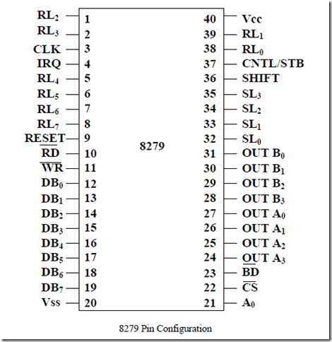
• The signal discription of each of the pins of 8279 as follows :
• DB0-DB7 : These are bidirectional data bus lines. The data and command words to and from the CPU are transferred on these lines.
• CLK : This is a clock input used to generate internal timing required by 8279.
• RESET : This pin is used to reset 8279. A high on this line reset 8279. After resetting 8279, its in sixteen 8-bit display, left entry encoded scan, 2-key lock out mode. The clock prescaler is set to 31.
• CS : Chip Select – A low on this line enables 8279 for normal read or write operations. Other wise, this pin should remain high.
• A0 : A high on this line indicates the transfer of a command or status information.
A low on this line indicates the transfer of data. This is used to select one of the internal registers of 8279.
• RD, WR (Input/Output) READ/WRITE – These input pins enable the data buffers to receive or send data over the data bus.
• IRQ : This interrupt output lines goes high when there is a data in the FIFO sensor RAM. The interrupt lines goes low with each FIFO RAM read operation but if the FIFO RAM further contains any key-code entry to be read by the CPU, this pin again goes high to generate an interrupt to the CPU.
• Vss, Vcc : These are the ground and power supply lines for the circuit.
• SL0-SL3-Scan Lines : These lines are used to scan the key board matrix and display digits. These lines can be programmed as encoded or decoded, using the mode control register.
• RL0 – RL7 – Return Lines : These are the input lines which are connected to one terminal of keys, while the other terminal of the keys are connected to the decoded scan lines. These are normally high, but pulled low when a key is pressed.
• SHIFT : The status of the shift input lines is stored along with each key code in FIFO, in scanned keyboard mode. It is pulled up internally to keep it high, till it is pulled low with a key closure.
• BD – Blank Display : This output pin is used to blank the display during digit switching or by a blanking closure.
• OUT A0 – OUT A3 and OUT B0 – OUT B3 – These are the output ports for two 16*4 or 16*8 internal display refresh registers. The data from these lines is synchronized with the scan lines to scan the display and keyboard. The two 4-bit ports may also as one 8-bit port.
• CNTL/STB- CONTROL/STROBED I/P Mode : In keyboard mode, this lines is used as a control input and stored in FIFO on a key closure. The line is a strobed lines that enters the data into FIFO RAM, in strobed input mode. It has an interrupt pull up. The lines is pulled down with a key closer.
Modes of Operation of 8279
• The modes of operation of 8279 are as follows :
1. Input (Keyboard) modes.
2. Output (Display) modes.
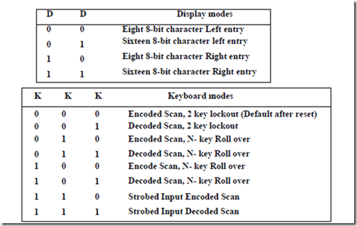
• Input (Keyboard) Modes : 8279 provides three input modes. These modes are as follows:
1. Scanned Keyboard Mode : This mode allows a key matrix to be interfaced using either encoded or decoded scans. In encoded scan, an 8*8 keyboard or in decoded scan, a 4*8 keyboard can be interfaced. The code of key pressed with SHIFT and CONTROL status is stored into the FIFO RAM.
2. Scanned Sensor Matrix : In this mode, a sensor array can be interfaced with 8279 using either encoded or decoded scans. With encoded scan 8*8 sensor matrix or with decoded scan 4*8 sensor matrix can be interfaced. The sensor codes are stored in the CPU addressable sensor RAM.
3. Strobed input: In this mode, if the control lines goes low, the data on return lines, is stored in the FIFO byte by byte.
• Output (Display) Modes : 8279 provides two output modes for selecting the display options. These are discussed briefly.
1. Display Scan : In this mode 8279 provides 8 or 16 character multiplexed displays those can be organized as dual 4- bit or single 8-bit display units.
2. Display Entry : (right entry or left entry mode) 8279 allows options for data entry on the displays. The display data is entered for display either from the right side or from the left side.
Keyboard Modes
i. Scanned Keyboard mode with 2 Key Lockout : In this mode of operation, when a key is pressed, a debounce logic comes into operation. During the next two scans, other keys are checked for closure and if no other key is pressed the first pressed key is identified.
• The key code of the identified key is entered into the FIFO with SHIFT and CNTL status, provided the FIFO is not full, i.e. it has at least one byte free. If the FIFO does not have any free byte, naturally the key data will not be entered and the error flag is set.
• If FIFO has at least one byte free, the above code is entered into it and the 8279 generates an interrupt on IRQ line to the CPU to inform about the previous key closures. If another key is found closed during the first key, the keycode is entered in FIFO.
• If the first pressed key is released before the others, the first will be ignored. A key code is entered to FIFO only once for each valid depression, independent of other keys pressed along with it, or released before it.
• If two keys are pressed within a debounce cycle (simultaneously), no key is recognized till one of them remains closed and the other is released. The last key, that remains depressed is considered as single valid key depression.
ii. Scanned Keyboard with N-Key Rollover : In this mode, each key depression is treated independently. When a key is pressed, the debounce circuit waits for 2 keyboards scans and then checks whether the key is still depressed. If it is still depressed, the code is entered in FIFO RAM.
Any number of keys can be pressed simultaneously and recognized in the order, the keyboard scan recorded them. All the codes of such keys are entered into FIFO.
In this mode, the first pressed key need not be released before the second is pressed. All the keys are sensed in the order of their depression, rather in the order the keyboard scan senses them, and independent of the order of their release.
iii. Scanned Keyboard Special Error Mode : This mode is valid only under the N- Key rollover mode. This mode is programmed using end interrupt / error mode set command. If during a single debounce period (two keyboard scans) two keys are found pressed , this is considered a simultaneous depression and an error flag is set.
• This flag, if set, prevents further writing in FIFO but allows the generation of further interrupts to the CPU for FIFO read. The error flag can be read by reading the FIFO status word. The error Flag is set by sending normal clear command with CF = 1.
iv. Sensor Matrix Mode : In the sensor matrix mode, the debounce logic is inhibited. The 8-byte FIFO RAM now acts as 8 * 8 bit memory matrix. The status of the sensor switch matrix is fed directly to sensor RAM matrix. Thus the sensor RAM bits contains the row-wise and column wise status of the sensors in the sensor matrix.
• The IRQ line goes high, if any change in sensor value is detected at the end of a sensor matrix scan or the sensor RAM has a previous entry to be read by the CPU. The IRQ line is reset by the first data read operation, if AI = 0, otherwise, by issuing the end interrupt command. AI is a bit in read sensor RAM word.
Display Modes
• There are various options of data display. For example, the command number of characters can be 8 or 16, with each character organised as single 8-bit or dual 4- bit codes. Similarly there are two display formats.
• The first one is known as left entry mode or type writer mode, since in a type writer the first character typed appears at the left-most position, while the subsequent characters appear successively to the right of the first one. The other display format is known as right entry mode, or calculator mode, since in a calculator the first character entered appears at the rightmost position and this character is shifted one position left when the next characters is entered.
• Thus all the previously entered characters are shifted left by one position when a new characters is entered.
i. Left Entry Mode : In the left entry mode, the data is entered from left side of the display unit. Address 0 of the display RAM contains the leftmost display characters and address 15 of the RAM contains the right most display characters. It is just like writing in our address is automatically updated with successive reads or writes. The first entry is displayed on the leftmost display and the sixteenth entry on the rightmost display. The seventeenth entry is again displayed at the leftmost display position.
ii. Right Entry Mode : In this right entry mode, the first entry to be displayed is entered on the rightmost display. The next entry is also placed in the right most display but after the previous display is shifted left by one display position. The leftmost characters is shifted out of that display at the seventeenth entry and is lost, i.e. it is pushed out of the display RAM.
Command Words of 8279
• All the command words or status words are written or read with A0 = 1 and CS = 0 to or from 8279. This section describes the various command available in 8279.
a) Keyboard Display Mode Set – The format of the command word to select different modes of operation of 8279 is given below with its bit definitions.
b) Programmable clock : The clock for operation of 8279 is obtained by dividing the external clock input signal by a programmable constant called prescaler.
• PPPPP is a 5-bit binary constant. The input frequency is divided by a decimal constant ranging from 2 to 31, decided by the bits of an internal prescaler, PPPPP.
c) Read FIFO / Sensor RAM : The format of this command is given below.
• This word is written to set up 8279 for reading FIFO/ sensor RAM. In scanned keyboard mode, AI and AAA bits are of no use. The 8279 will automatically drive data bus for each subsequent read, in the same sequence, in which the data was entered.
• In sensor matrix mode, the bits AAA select one of the 8 rows of RAM. If AI flag is set, each successive read will be from the subsequent RAM location.
X – don’t care
AI – Auto Increment Flag
AAA – Address pointer to 8 bit FIFO RAM
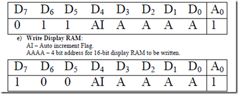
d) Read Display RAM : This command enables a programmer to read the display RAM data. The CPU writes this command word to 8279 to prepare it for display RAM read operation. AI is auto increment flag and AAAA, the 4-bit address points to the 16-byte display RAM that is to be read. If AI=1, the address will be automatically, incremented after each read or write to the Display RAM. The same address counter is used for reading and writing.
f) Display Write Inhibit/Blanking : The IW (inhibit write flag) bits are used to mask the individual nibble as shown in the below command word. The output lines are divided into two nibbles (OUTA0 – OUTA3) and (OUTB0 – OUTB3), those can be masked by setting the corresponding IW bit to 1.
• Once a nibble is masked by setting the corresponding IW bit to 1, the entry to display RAM does not affect the nibble even though it may change the unmasked nibble. The blank display bit flags (BL) are used for blanking A and B nibbles.
• Here D0, D2 corresponds to OUTB0 – OUTB3 while D1 and D3 corresponds to OUTA0-OUTA3 for blanking and masking.
• If the user wants to clear the display, blank (BL) bits are available for each nibble as shown in format. Both BL bits will have to be cleared for blanking both the nibbles.
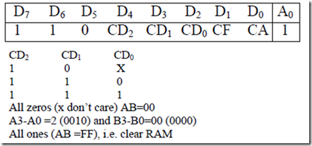
g) Clear Display RAM : The CD2, CD1, CD0 is a selectable blanking code to clear all the rows of the display RAM as given below. The characters A and B represents the output nibbles.
• CD2 must be 1 for enabling the clear display command. If CD2 = 0, the clear display command is invoked by setting CA=1 and maintaining CD1, CD0 bits exactly same as above. If CF=1, FIFO status is cleared and IRQ line is pulled down.
• Also the sensor RAM pointer is set to row 0. if CA=1, this combines the effect of CD and CF bits. Here, CA represents Clear All and CF as Clear FIFO RAM.
h) End Interrupt / Error mode Set : For the sensor matrix mode, this command lowers the IRQ line and enables further writing into the RAM. Otherwise, if a change in sensor value is detected, IRQ goes high that inhibits writing in the sensor RAM.
• For N-Key roll over mode, if the E bit is programmed to be ‘1’, the 8279 operates in special Error mode. Details of this mode are described in scanned keyboard special error mode. X– don’t care.
If we are working with an 8086, we have a problem here because the 8086 has only two interrupt inputs, NMI and INTR.
• If we save NMI for a power failure interrupt, this leaves only one interrupt for all the other applications. For applications where we have interrupts from multiple source, we use an external device called a priority interrupt controller (PIC) to the interrupt signals into a single interrupt input on the processor.
Architecture and Signal Descriptions of 8259A
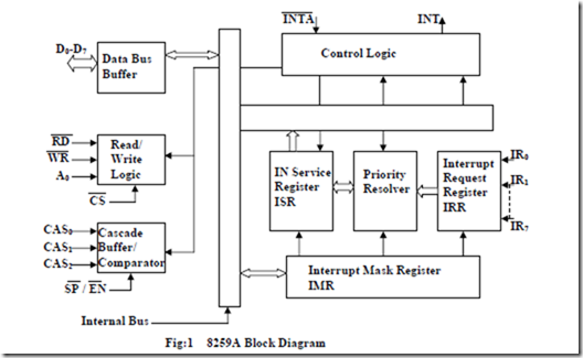
• The architectural block diagram of 8259A is shown in fig1. The functional explication of each block is given in the following text in brief.
• Interrupt Request Register (RR): The interrupts at IRQ input lines are handled by Interrupt Request internally. IRR stores all the interrupt request in it in order to serve them one by one on the priority basis.
• In-Service Register (ISR): This stores all the interrupt requests those are being served, i.e. ISR keeps a track of the requests being served.
• Priority Resolver : This unit determines the priorities of the interrupt requests appearing simultaneously. The highest priority is selected and stored into the corresponding bit of ISR during INTA pulse. The IR0 has the highest priority while the IR7 has the lowest one, normally in fixed priority mode. The priorities however may be altered by programming the 8259A in rotating priority mode.
• Interrupt Mask Register (IMR) : This register stores the bits required to mask the interrupt inputs. IMR operates on IRR at the direction of the Priority Resolver.
• Interrupt Control Logic: This block manages the interrupt and interrupt acknowledge signals to be sent to the CPU for serving one of the eight interrupt requests. This also accepts the interrupt acknowledge (INTA) signal from CPU that causes the 8259A to release vector address on to the data bus.
• Data Bus Buffer : This tristate bidirectional buffer interfaces internal 8259A bus to the microprocessor system data bus. Control words, status and vector information pass through data buffer during read or write operations.
• Read/Write Control Logic: This circuit accepts and decodes commands from the CPU. This block also allows the status of the 8259A to be transferred on to the data bus.
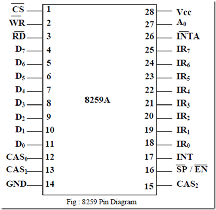
• Cascade Buffer/Comparator: This block stores and compares the ID’s all the 8259A used in system. The three I/O pins CASO-2 are outputs when the 8259A is used as a master. The same pins act as inputs when the 8259A is in slave mode. The 8259A in master mode sends the ID of the interrupting slave device on these lines. The slave thus selected, will send its preprogrammed vector address on the data bus during the next INTA pulse.
• CS: This is an active-low chip select signal for enabling RD and WR operations of 8259A. INTA function is independent of CS.
• WR : This pin is an active-low write enable input to 8259A. This enables it to accept command words from CPU.
• RD : This is an active-low read enable input to 8259A. A low on this line enables 8259A to release status onto the data bus of CPU.
• D0-D7 : These pins from a bidirectional data bus that carries 8-bit data either to control word or from status word registers. This also carries interrupt vector information.
• CAS0 – CAS2 Cascade Lines : A signal 8259A provides eight vectored interrupts. If more interrupts are required, the 8259A is used in cascade mode. In cascade mode, a master 8259A along with eight slaves 8259A can provide upto 64 vectored interrupt lines. These three lines act as select lines for addressing the slave 8259A.
• PS/EN : This pin is a dual purpose pin. When the chip is used in buffered mode, it can be used as buffered enable to control buffer transreceivers. If this is not used in buffered mode then the pin is used as input to designate whether the chip is used as a master (SP =1) or slave (EN = 0).
• INT : This pin goes high whenever a valid interrupt request is asserted. This is used to interrupt the CPU and is connected to the interrupt input of CPU.
• IR0 – IR7 (Interrupt requests) :These pins act as inputs to accept interrupt request to the CPU. In edge triggered mode, an interrupt service is requested by raising an IR pin from a low to a high state and holding it high until it is acknowledged, and just by latching it to high level, if used in level triggered mode.
• INTA (Interrupt acknowledge): This pin is an input used to strobe-in 8259A interrupt vector data on to the data bus. In conjunction with CS, WR and RD pins, this selects the different operations like, writing command words, reading status word, etc.
• The device 8259A can be interfaced with any CPU using either polling or interrupt. In polling, the CPU keeps on checking each peripheral device in sequence to ascertain if it requires any service from the CPU. If any such service request is noticed, the CPU serves the request and then goes on to the next device in sequence.
• After all the peripheral device are scanned as above the CPU again starts from first device.
• This type of system operation results in the reduction of processing speed because most of the CPU time is consumed in polling the peripheral devices.
• In the interrupt driven method, the CPU performs the main processing task till it is interrupted by a service requesting peripheral device.
• The net processing speed of these type of systems is high because the CPU serves the peripheral only if it receives the interrupt request.
• If more than one interrupt requests are received at a time, all the requesting peripherals are served one by one on priority basis.
• This method of interfacing may require additional hardware if number of peripherals to be interfaced is more than the interrupt pins available with the CPU.
Interrupt Sequence in an 8086 system
• The Interrupt sequence in an 8086-8259A system is described as follows:
1. One or more IR lines are raised high that set corresponding IRR bits.
2. 8259A resolves priority and sends an INT signal to CPU.
3. The CPU acknowledge with INTA pulse.
4. Upon receiving an INTA signal from the CPU, the highest priority ISR bit is set and the corresponding IRR bit is reset. The 8259A does not drive data during this period.
5. The 8086 will initiate a second INTA pulse. During this period 8259A releases an 8-bit pointer on to a data bus from where it is read by the CPU.
6. This completes the interrupt cycle. The ISR bit is reset at the end of the second INTA pulse if automatic end of interrupt (AEOI) mode is programmed. Otherwise ISR bit remains set until an appropriate EOI command is issued at the end of interrupt subroutine.
Command Words of 8259A
• The command words of 8259A are classified in two groups
1. Initialization command words (ICW) and
2. Operation command words (OCW).
• Initialization Command Words (ICW): Before it starts functioning, the 8259A must be initialized by writing two to four command words into the respective command word registers. These are called as initialized command words.
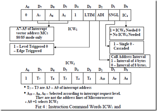
• If A0 = 0 and D4 = 1, the control word is recognized as ICW1. It contains the control bits for edge/level triggered mode, single/cascade mode, call address interval and whether ICW4 is required or not.
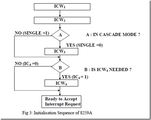
• If A0=1, the control word is recognized as ICW2. The ICW2 stores details regarding interrupt vector addresses. The initialisation sequence of 8259A is described in form of a flow chart in fig 3 below.
• The bit functions of the ICW1 and ICW2 are self explanatory as shown in fig below.
• Once ICW1 is loaded, the following initialization procedure is carried out internally.
a. The edge sense circuit is reset, i.e. by default 8259A interrupts are edge sensitive.
b. IMR is cleared.
c. IR7 input is assigned the lowest priority.
d. Slave mode address is set to 7.
e. Special mask mode is cleared and status read is set to IRR.
f. If IC4 = 0, all the functions of ICW4 are set to zero. Master/Slave bit in ICW4 is used in the buffered mode only.
g. In an 8085 based system A15-A8 of the interrupt vector address are the respective bits of ICW2.
h. In 8086 based system A15-A11 of the interrupt vector address are inserted in place of T7 – T3 respectively and the remaining three bits A8, A9, A10 are selected depending upon the interrupt level, i.e. from 000 to 111 for IR0 to IR7.
i. ICW1 and ICW2 are compulsory command words in initialization sequence of 8259A as is evident from fig, while ICW3 and ICW4 are optional. The ICW3 is read only when there are more than one 8259A in the system, cascading is used (SNGL=0).
j. The SNGL bit in ICW1 indicates whether the 8259A in the cascade mode or not.
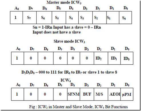
The ICW3 loads an 8-bit slave register. It detailed functions are as follows.
k. In master mode [ SP = 1 or in buffer mode M/S = 1 in ICW4], the 8-bit slave register will be set bit-wise to 1 for each slave in the system as in fig 5.
l. The requesting slave will then release the second byte of a CALL sequence. In slave mode [ SP=0 or if BUF =1 and M/S = 0 in ICW4] bits D2 to D0 identify the slave, i.e. 000 to 111 for slave 1 to slave 8. The slave compares the cascade inputs with these bits and if they are equal, the second byte of the CALL sequence is released by it on the data bus.
• ICW4: The use of this command word depends on the IC4 bit of ICW1. If IC4=1, IC4 is used, otherwise it is neglected. The bit functions of ICW4 are described as follow:
• SFNM: If BUF = 1, the buffered mode is selected. In the buffered mode, SP/EN acts as enable output and the master/slave is determined using the M/S bit of ICW4.
• M/S: If M/S = 1, 8259A is a master. If M/S =0, 8259A is slave. If BUF = 0, M/S is to be neglected.
• AEOI: If AEOI = 1, the automatic end of interrupt mode is selected.
• µPM : If the µPM bit is 0, the Mcs-85 system operation is selected and if µPM=1, 8086/88 operation is selected.
• Operation Command Words: Once 8259A is initialized using the previously discussed command words for initialisation, it is ready for its normal function, i.e. for accepting the interrupts but 8259A has its own way of handling the received
interrupts called as modes of operation. These modes of operations can be selected by programming, i.e. writing three internal registers called as operation command words.
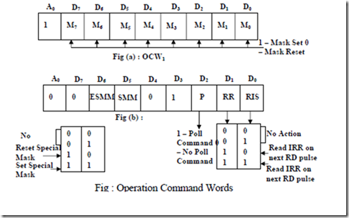
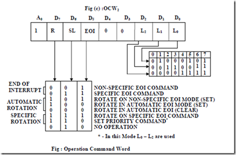
• In the three operation command words OCW1, OCW2 and OCW3 every bit corresponds to some operational feature of the mode selected, except for a few bits those are either 1 or 0. The three operation command words are shown in fig with the bit selection details.
• OCW1 is used to mask the masked and if it is 0 the request is enabled. In OCW2 the three bits, R, SL and EOI control the end of interrupt, the rotate mode and their combinations as shown in fig below.
• The three bits L2, L1 and L0 in OCW2 determine the interrupt level to be selected for operation, if SL bit is active i.e. 1.
• The details of OCW2 are shown in fig.
• In operation command word 3 (OCW3), if the ESMM bit, i.e. enable special mask mode bit is set to 1, the SMM bit is neglected. If the SMM bit, i.e. special mask mode. When ESMM bit is 0 the SMM bit is neglected. If the SMM bit. i.e. special mask mode bit is 1, the 8259A will enter special mask mode provided ESMM=1.
• If ESMM=1 and SMM=0, the 8259A will return to the normal mask mode. The details of bits of OCW3 are given in fig along with their bit definitions.
Operating Modes of 8259
• The different modes of operation of 8259A can be programmed by setting or resting the appropriate bits of the ICW or OCW as discussed previously. The different modes of operation of 8259A are explained in the following.
• Fully Nested Mode : This is the default mode of operation of 8259A. IR0 has the highest priority and IR7 has the lowest one. When interrupt request are noticed, the highest priority request amongst them is determined and the vector is placed on the data bus. The corresponding bit of ISR is set and remains set till the microprocessor issues an EOI command just before returning from the service routine or the AEOI bit is set.
• If the ISR (in service) bit is set, all the same or lower priority interrupts are inhibited but higher levels will generate an interrupt, that will be acknowledge only if the microprocessor interrupt enable flag IF is set. The priorities can afterwards be changed by programming the rotating priority modes.
• End of Interrupt (EOI) : The ISR bit can be reset either with AEOI bit of ICW1 or by EOI command, issued before returning from the interrupt service routine. There are two types of EOI commands specific and non-specific. When 8259A is operated in the modes that preserve fully nested structure, it can determine which ISR bit is to be reset on EOI.
• When non-specific EOI command is issued to 8259A it will be automatically reset the highest ISR bit out of those already set.
• When a mode that may disturb the fully nested structure is used, the 8259A is no longer able to determine the last level acknowledged. In this case a specific EOI command is issued to reset a particular ISR bit. An ISR bit that is masked by the
corresponding IMR bit, will not be cleared by non-specific EOI of 8259A, if it is in special mask mode.
• Automatic Rotation : This is used in the applications where all the interrupting devices are of equal priority.
• In this mode, an interrupt request IR level receives priority after it is served while the next device to be served gets the highest priority in sequence. Once all the device are served like this, the first device again receives highest priority.
• Automatic EOI Mode : Till AEOI=1 in ICW4, the 8259A operates in AEOI mode. In this mode, the 8259A performs a non-specific EOI operation at the trailing edge of the last INTA pulse automatically. This mode should be used only when a nested multilevel interrupt structure is not required with a single 8259A.
• Specific Rotation : In this mode a bottom priority level can be selected, using L2, L1 and L0 in OCW2 and R=1, SL=1, EOI=0.
• The selected bottom priority fixes other priorities. If IR5 is selected as a bottom priority, then IR5 will have least priority and IR4 will have a next higher priority. Thus IR6 will have the highest priority.
• These priorities can be changed during an EOI command by programming the rotate on specific EOI command in OCW2.
• Specific Mask Mode: In specific mask mode, when a mask bit is set in OCW1, it inhibits further interrupts at that level and enables interrupt from other levels, which are not masked.
• Edge and Level Triggered Mode : This mode decides whether the interrupt should be edge triggered or level triggered. If bit LTIM of ICW1 =0 they are edge triggered, otherwise the interrupts are level triggered.
• Reading 8259 Status : The status of the internal registers of 8259A can be read using this mode. The OCW3 is used to read IRR and ISR while OCW1 is used to read IMR. Reading is possible only in no polled mode.
• Poll Command : In polled mode of operation, the INT output of 8259A is neglected, though it functions normally, by not connecting INT output or by masking INT input of the microprocessor. The poll mode is entered by setting P=1 in OCW3.
• The 8259A is polled by using software execution by microprocessor instead of the requests on INT input. The 8259A treats the next RD pulse to the 8259A as an interrupt acknowledge. An appropriate ISR bit is set, if there is a request. The priority level is read and a data word is placed on to data bus, after RD is activated. A poll command may give more than 64 priority levels.
• Special Fully Nested Mode : This mode is used in more complicated system, where cascading is used and the priority has to be programmed in the master using ICW4. this is somewhat similar to the normal nested mode.
• In this mode, when an interrupt request from a certain slave is in service, this slave can further send request to the master, if the requesting device connected to the slave has higher priority than the one being currently served. In this mode, the master interrupt the CPU only when the interrupting device has a higher or the same priority than the one current being served. In normal mode, other requests than the one being served are masked out.
• When entering the interrupt service routine the software has to check whether this is the only request from the slave. This is done by sending a non-specific EOI can be sent to the master, otherwise no EOI should be sent. This mode is important, since in the absence of this mode, the slave would interrupt the master only once and hence the priorities of the slave inputs would have been disturbed.
• Buffered Mode: When the 83259A is used in the systems where bus driving buffers are used on data buses. The problem of enabling the buffers exists. The 8259A sends buffer enable signal on SP/ EN pin, whenever data is placed on the bus.
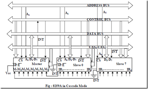
• Cascade Mode : The 8259A can be connected in a system containing one master and eight slaves (maximum) to handle upto 64 priority levels. The master controls the slaves using CAS0-CAS2 which act as chip select inputs (encoded) for slaves.
• In this mode, the slave INT outputs are connected with master IR inputs. When a slave request line is activated and acknowledged, the master will enable the slave to release the vector address during second pulse of INTA sequence.
• The cascade lines are normally low and contain slave address codes from the trailing edge of the first INTA pulse to the trailing edge of the second INTA pulse. Each 8259A in the system must be separately initialized and programmed to work in different modes. The EOI command must be issued twice, one for master and the other for the slave.
• A separate address decoder is used to activate the chip select line of each 8259A.
• Following Fig shows the details of the circuit connections of 8259A in cascade scheme.
