Architecture
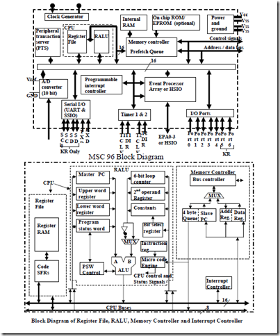
• The MCS-96 supports a complete instruction set which includes bit operations, byte operations, word operations, double-word operations (unsigned 32 bit), long operations (signed 32 bit), flag manipulations as well as jump and call instructions.
• All the standard logical and arithmetic instructions function as both byte and word operations.
• The jump bit set and jump bit clear instructions can operate on any of the SFR or bytes in the lower register files. These fast bit manipulations allow for rapid I/O functions.
• Byte and word operations make up the instruction set. The assembly language ASM-96 uses a “B” suffix on a mnemonic for a byte operation or for word operation.
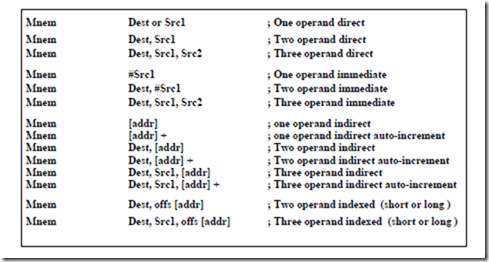
• Addressing modes: This supports the following modes.
• Register-direct, indirect, indirect with auto-increment, immediate, short-indexed and long-indexed.
• These modes increase the flexibility and overall execution speed of the MCS-96 devices.
Instruction Format
8096 Peripherals
• Standard I/O Ports – The 8096 has five 8 bit I/O ports.
• Port 0 is an input port that is also the analog input for the A/D converter.
• Port 1 is a quasi-bidirectional port.
• Port 2 contains three types of port lines.
• Quasi-Bidirectional, input and output. Other functions on the 8096 share the input and output lines with Port 2.
• Port 3 and 4 are open-drain bidirectional ports that share their pins with the address/data bus.
• Timers – The 8096 has two 16 bit timers. Timer 1 and Timer 2.
• An internal clock increments the Timer 1 value every 8 state times. (A state time is 3 oscillator periods)
• An external clock increments Timer 2 on every positive and negative transition.
• Either an internal or external source can reset Timer 2.
• This two timers can generate an interrupt when crossing the 0FFFFH/0000H boundary.
• The 8096 includes separate, dedicated timers for serial port baud rate generator and watchdog timer.
• The watchdog Timer is an internal timer that resets the system if the software fails to operate properly.
• High Speed Input Unit (HSI) – The 8096 HIS unit can record times of external events with a 9 state time resolution. It can monitor four independently configurable HSI lines and captures the value of timer 1 when events takes place.
• The four types of events that can trigger captures include: rising edge only, falling edge only, rising or falling edges, or every eight rising edge.
• The HSI unit can store upto 8 entries (Timer 1 values ).
• Reading the HSI holding register unloads the earliest entry placed in the FIFO.
• The HSI unit can generate an interrupt when loading an entry into the HSI holding register or loading the sixth entry into the FIFO.
• High Speed Output Unit (HSO) – The 8096 HSO unit can trigger events at specified times based on Timer1 or Timer2.
• These programmable events include: starting an A/D conversion, resetting Timer2, generating up to four software time delays, and setting or clearing one or more of the six HSO output lines.
• The HSO unit stores pending event and specified times in a Content Addressable Memory (CAM) file. This file stores up to 8 commands.
• Each command specifies the action time, the nature of the action, whether an interrupt is to occur, and whether Timer1 or Timer2 is the reference timer.
• Every 8 state times the HSO compares the CAM locations for time matches. The HSO unit triggers the specified event when it finds a time match.
• A command is cleared from the CAM as soon as it executes.
• Serial Port – The serial port on the 8096 has one synchronous (Mode 0) and three asynchronous modes (Modes 1, 2 and 3).
• The asynchronous modes are full duplex.
• Mode 0, the synchronous mode, is to expand the I/O capability of the 8096 using shift register.
• Mode 1 is the standard asynchronous mode used for normal serial communication.
• Modes 2, 3 are 9-bit modes commonly used for multiprocessor communications.
• Pulse Width Modulator (PWM) – The PWM output waveform is a variable duty cycle pulse that repeats every 256 state times.
• The PWM output can perform digital to analog conversions and drive several types of motors that require a PWM waveform for more efficient operation.
• A/D Converter – The 8096 A/D converts an analog input to a 10 bit digital equivalent.
• The main components of the A/D Converter are: 8 analog inputs, an 8 to 1 multiplexer, a sample and hold capacitor and resistor ladder.
• The A/D Converter can start a conversion immediately or the High Speed Output unit can trigger a conversion at a preprogrammed time.
• The A/D converter performs a conversion in 88 state times. Upon completion of each conversion the converter can generate a conversion complete interrupt.
• The 8X9X provides separate VREF and ANGND supply pins to isolate noise on the Vcc or Vss lines.
• Interrupts – There are 21 interrupts sources and 8 interrupt vector on the 8096.
• When the interrupt controller detects one of the 8 interrupts it sets the corresponding bit in the interrupt pending register. Individual interrupts are enabled or disabled by setting or clearing bits in the interrupt mask register.
• When the interrupt controller decides to process an interrupt, it executes a “call” to an interrupt service routine ISR. The corresponding interrupt vector contains the address of the ISR. The interrupt controller then clears the associated pending bit.
Chip configuration byte (CCB)
Configuring the 8096
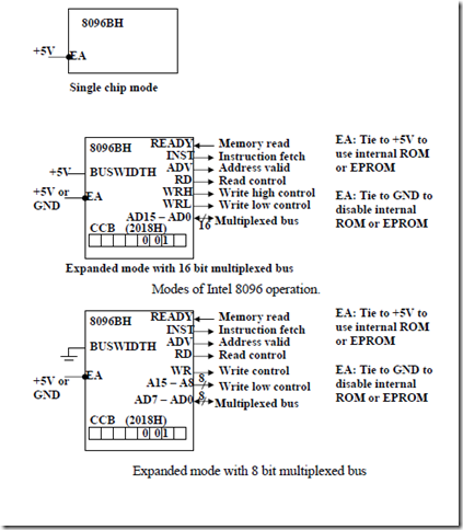
• The 8096 can be operated in either the single-chip mode, or two of its ports can be redefined to bring out the internal address bus and data bus.
• For the single chip mode, the internal ROM and EPROM must be accessed. This choice is made by tying the EA# pin high.
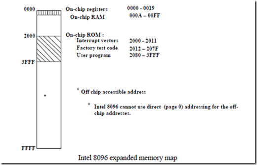
• When EA pin is tied high, the internal ROM or EPROM is accessed during instruction and data fetches from addresses 2080 to 3FFFH and for interrupt vectors located at addresses 2000 to 2011H.
• When operated in the expanded mode the internal ROM or EPROM can still be used by tying EA# high.
• Accesses to the addresses 2000 to 2011H and 2080 to 3FFFH can be made to access off-chip memory by tying the EA# pin low.
• If the EA pin is high, then we have the option of using the internal ROM or EPROM together with external memory and devices.
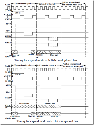
• One of the options made available by the BH series over the original 8096 family is the option to deal with either a 16 bit external data bus or else an 8 bit external data bus.
• The latter options permits expanding the 8096 with a single byte wide static RAM chip or with a single byte wide EPROM chip for program memory.
• The latter is particularly convenient for users who can either put their application program into a single EPROM or who do not have the EPROM programming capability to separate their object code into even addresses and odd addresses as required for the two byte wide EPROM used with a 16 bit data bus.
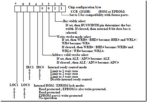
• The choice of bus width is made in two places. When the 8096 comes out of reset, it reads the content of address 2018H of our ROM or EPROM. This is called the chip configuration CCB.
• The 8096 stores this byte in a chip configuration register which is unaccessable by our software.
• Bit 1 works together with the external BUSWIDTH pin to determine the data bus width (when the EA pin is tied low).
• While the BUSWIDTH pin is tied either high or low, it can actually be changed during each bus cycle of normal operation.
• If it is tied to the A15 address lines, then accesses to external addresses 8000 to FFFFH would use a 16-bit data bus while accesses to external addresses below this would use an 8-bit data bus. In either case, the full 16 bit address bus is brought out.
• When an 8-bit data bus is brought out, the lines which bring out the upper half of the address bus do not have to be multiplexed.
• In this case, the designers of the chip have saved users the need for an external latch for the upper half of the address bus by latching the address internally.
• The original 8096 parts gave the user of the expanded chip an ALE output. This was used to latch the address. The new option is selected with a 0 in bit 3 of CCB. The ADV# line remains high during any machine cycles which are not accessing external memory, but goes low during external accesses. Because of this ADV# can be used to simplify the decoding to enable external devices.
• In addition to the external access, ADV# drop low at precisely the current time to latch the multiplexed address. Consequently, it can serve double duty, both helping with decoding and also latching the multiplexed address.
• Another feature of the original 8096 parts operating in the expanded mode was the need to decode a BHE# signal.
• This was used during writes to a byte at an odd address so that the lower byte on the 16-bit data bus could be left unchanged.
• Users of the original 8096 parts had to gate BHE# together with a WR# signal to generate two write signals.
• One for chips connected to the upper half of the data bus and one for chip connected to the lower half of the data bus.
• This option is selected with 0 bit 2 of CCB.
• INST output is a signal which takes on when the RD# line is active, signaling that a read from an external device is taking place. If the read is an instruction fetch, then INST will be high. Otherwise it will be low during the read cycle.
• Users of logia analyzers and designers of 8096 emulators can use this signal to help sort out the activity on external bus.
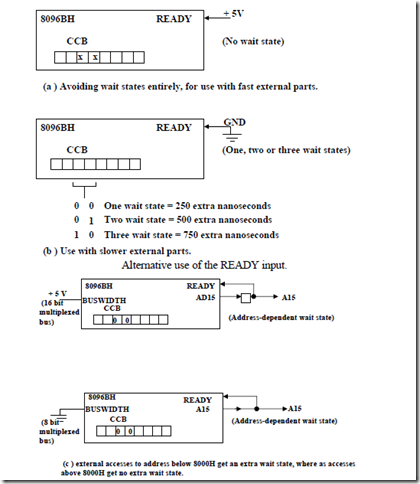
• The READY control line permits the 8096 to run at full speed for its internal accesses and yet to slow down for some of its external accesses.
• It is used in conjunction with bits 4 and 5 of CCB to introduce extra 250ns (assuming a 12 MHz crystal) wait states into external read and write cycles.
• If the READY line is tied high then the CCB bits do not matter and no external wait states are introduced into external read or writes.
• If the READY line is tied low (signifying that external devices are not ready), then this READY signal can be overridden by the CCB bits.
• Thus 00 in bits 4 and 5 of CCB will now limit the delay to a signal wait state.
• READY line can be changed by dynamically from cycle to cycle. If it is tied to the upper address lines, then we can position external devices which can run at full speed in the 8000 to FFFF address range and slower external device needing an extra wait state at lower addresses.
• The lock mode is selected by the coding of bit 6 and 7. Whether the software is in on-chip manage to get the chip to execute code from external memory and then have that external program dump the internal memory to the serial port.
• In a read-protected mode, only code executing from internal memory can read from memory addresses between 2020 to 3FFFH.
• In a write-protected mode, no code can write to memory address between 2000 and 3FFFH.
• One problem arises with a memory protection scheme such as, if we purchase ROM-protected parts from Intel, then before we use them, we would like to test them.
• We can drive the EA# line low and use our own program to test all the resource on the chip. This does not test the ROM contents.
• Intel supports the verification of ROM by including a 16byte security key, located at address 2020 to 202FH. Before protected memory can read, the chip must read external memory locations 4020 to 402FH and compare the contents with the internal security key.
• Access to protected memory will only be allowed if a match I found for all 16 bytes.
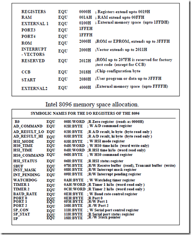
• The first 26 addresses from the register file, used to set up and access almost all of the on-chip resources. The rest of the page 0 is dedicated to internal RAM, for a total of 230 bytes of RAM.
• While the ROM or EPROM extends from 2000 to 3FFFH, Intel reserves address 2012 to 2017H.
