Module 3 Learning unit 8:
Interface
• We have four common types of memory:
• Read only memory (ROM)
• Flash memory (EEPROM)
• Static Random access memory (SARAM)
• Dynamic Random access memory (DRAM).
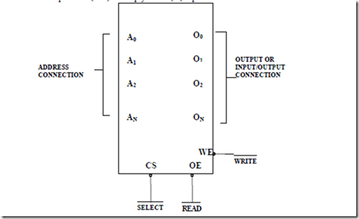
• Pin connections common to all memory devices are: The address input, data output or input/outputs, selection input and control input used to select a read or write operation.
• Address connections: All memory devices have address inputs that select a memory location within the memory device. Address inputs are labeled from A0 to An.
• Data connections: All memory devices have a set of data outputs or input/outputs. Today many of them have bi-directional common I/O pins.
• Selection connections: Each memory device has an input, that selects or enables the memory device. This kind of input is most often called a chip select ( CS ), chip enable ( CE ) or simply select ( S ) input.
MEMORY COMPONENT ILLUSTRATING THE ADDRESS, DATA AND CONTROL CONNECTIONS
• RAM memory generally has at least one CS or S input and ROM at least one CE .
• If the CE , CS , S input is active the memory device perform the read or write.
• If it is inactive the memory device cannot perform read or write operation.
• If more than one CS connection is present, all most be active to perform read or write data.
• Control connections: A ROM usually has only one control input, while a RAM often has one or two control inputs.
• The control input most often found on the ROM is the output enable ( OE ) or gate ( G ), this allows data to flow out of the output data pins of the ROM.
• If OE and the selected input are both active, then the output is enable, if OE is
inactive, the output is disabled at its high-impedance state.
• The OE connection enables and disables a set of three-state buffer located within the memory device and must be active to read data.
• A RAM memory device has either one or two control inputs. If there is one control input it is often called R/ W .
• This pin selects a read operation or a write operation only if the device is selected by the selection input ( CS ).
• If the RAM has two control inputs, they are usually labeled WE or W and OE or G .
• ( WE ) write enable must be active to perform a memory write operation and OE must be active to perform a memory read operation.
• When these two controls WE and OE are present, they must never be active at the same time.
• The ROM read only memory permanently stores programs and data and data was always present, even when power is disconnected.
• It is also called as nonvolatile memory.
• EPROM (erasable programmable read only memory) is also erasable if exposed to high intensity ultraviolet light for about 20 minutes or less, depending upon the type of EPROM.
• We have PROM (programmable read only memory)
• RMM (read mostly memory) is also called the flash memory.
• The flash memory is also called as an EEPROM (electrically erasable programmable ROM), EAROM (electrically alterable ROM), or a NOVROM (nonvolatile ROM).
• These memory devices are electrically erasable in the system, but require more time to erase than a normal RAM.
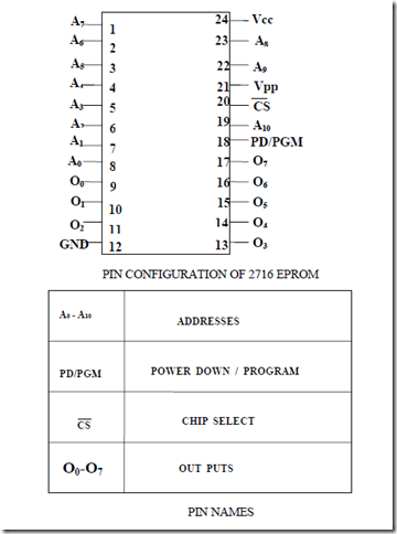
• EPROM contains the series of 27XXX contains the following part numbers : 2704(512 * 8), 2708(1K * 8), 2716(2K * 8), 2732(4K * 8), 2764(8K * 8),
27128(16K * 8) etc.
• Each of these parts contains address pins, eight data connections, one or more chip selection inputs ( CE ) and an output enable pin ( OE ).
• This device contains 11 address inputs and 8 data outputs.
• If both the pin connection CE and OE are at logic 0, data will appear on the output connection . If both the pins are not at logic 0, the data output connections remains at their high impedance or off state.
• To read data from the EPROM Vpp pin must be placed at a logic 1.
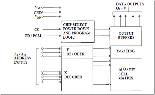
BLOCK DIAGRAM
• Static RAM memory device retain data for as long as DC power is applied.
Because no special action is required to retain stored data, these devices are called as static memory. They are also called volatile memory because they will not retain data without power.
• The main difference between a ROM and RAM is that a RAM is written under normal operation, while ROM is programmed outside the computer and is only normally read.
• The SRAM stores temporary data and is used when the size of read/write memory is relatively small.
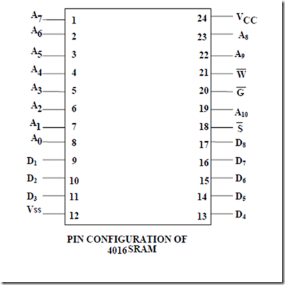
PIN NAMES
The control inputs of this RAM are slightly different from those presented earlier. The OE pin is labeled G , the CS pin S and the WE pin W .
• This 4016 SRAM device has 11 address inputs and 8 data input/output connections.
Static RAM Interfacing
• The semiconductor RAM is broadly two types – Static RAM and Dynamic RAM.
• The semiconductor memories are organised as two dimensional arrays of memory locations.
• For example 4K * 8 or 4K byte memory contains 4096 locations, where each locations contains 8-bit data and only one of the 4096 locations can be selected at a time. Once a location is selected all the bits in it are accessible using a group of conductors called Data bus.
• For addressing the 4K bytes of memory, 12 address lines are required.
• In general to address a memory location out of N memory locations, we will require at least n bits of address, i.e. n address lines where n = Log2 N.
• Thus if the microprocessor has n address lines, then it is able to address at the most N locations of memory, where 2n=N. If out of N locations only P memory locations are to be interfaced, then the least significant p address lines out of the
available n lines can be directly connected from the microprocessor to the memory chip while the remaining (n-p) higher order address lines may be used for address decoding as inputs to the chip selection logic.
• The memory address depends upon the hardware circuit used for decoding the chip select ( CS ). The output of the decoding circuit is connected with the CS pin of the memory chip.
• The general procedure of static memory interfacing with 8086 is briefly described as follows:
1. Arrange the available memory chip so as to obtain 16- bit data bus width. The upper 8-bit bank is called as odd address memory bank and the lower 8-bit bank is called as even address memory bank.
2. Connect available memory address lines of memory chip with those of the microprocessor and also connect the memory RD and WR inputs to the corresponding processor control signals. Connect the 16-bit data bus of the memory bank with that of the microprocessor 8086.
3. The remaining address lines of the microprocessor, BHE and A0 are used for decoding the required chip select signals for the odd and even memory banks. The CS of memory is derived from the o/p of the decoding circuit.
• As a good and efficient interfacing practice, the address map of the system should be continuous as far as possible, i.e. there should not be no windows in the map and no fold back space should be allowed.
• A memory location should have a single address corresponding to it, i.e. absolute decoding should be preferred and minimum hardware should be used for decoding.
Dynamic RAM
• Whenever a large capacity memory is required in a microcomputer system, the memory subsystem is generally designed using dynamic RAM because there are various advantages of dynamic RAM.
• E.g. higher packing density, lower cost and less power consumption. A typical static RAM cell may require six transistors while the dynamic RAM cell requires only a transistors along with a capacitor. Hence it is possible to obtain higher packaging density and hence low cost units are available.
• The basic dynamic RAM cell uses a capacitor to store the charge as a representation of data. This capacitor is manufactured as a diode that is reverse- biased so that the storage capacitance comes into the picture.
• This storage capacitance is utilized for storing the charge representation of data but the reverse-biased diode has leakage current that tends to discharge the capacitor giving rise to the possibility of data loss. To avoid this possible data loss, the data stored in a dynamic RAM cell must be refreshed after a fixed time interval regularly. The process of refreshing the data in RAM is called as Refresh cycle.
• The refresh activity is similar to reading the data from each and every cell of memory, independent of the requirement of microprocessor. During this refresh period all other operations related to the memory subsystem are suspended. Hence the refresh activity causes loss of time, resulting in reduce system performance.
• However keeping in view the advantages of dynamic RAM, like low power consumption, high packaging density and low cost, most of the advanced computing system are designed using dynamic RAM, at the cost of operating speed.
• A dedicated hardware chip called as dynamic RAM controller is the most important part of the interfacing circuit.
• The Refresh cycle is different from the memory read cycle in the following aspects.
1. The memory address is not provided by the CPU address bus, rather it is generated by a refresh mechanism counter called as refresh counter.
2. Unlike memory read cycle, more than one memory chip may be enabled at a time so as to reduce the number of total memory refresh cycles.
3. The data enable control of the selected memory chip is deactivated, and data is not allowed to appear on the system data bus during refresh, as more than one memory units are refreshed simultaneously. This is to avoid the data from the different chips to appear on the bus simultaneously.
4. Memory read is either a processor initiated or an external bus master initiated and carried out by the refresh mechanism.
• Dynamic RAM is available in units of several kilobits to megabits of memory.
This memory is arranged internally in a two dimensional matrix array so that it will have n rows and m columns. The row address n and column address m are important for the refreshing operation.
• For example, a typical 4K bit dynamic RAM chip has an internally arranged bit array of dimension 64 * 64 , i.e. 64 rows and 64 columns. The row address and column address will require 6 bits each. These 6 bits for each row address and column address will be generated by the refresh counter, during the refresh cycles.
• A complete row of 64 cells is refreshed at a time to minimizes the refreshing time.
Thus the refresh counter needs to generate only row addresses. The row address are multiplexed, over lower order address lines.
• The refresh signals act to control the multiplexer, i.e. when refresh cycle is in process the refresh counter puts the row address over the address bus for refreshing. Otherwise, the address bus of the processor is connected to the address bus of DRAM, during normal processor initiated activities.
• A timer, called refresh timer, derives a pulse for refreshing action after each refresh interval.
• Refresh interval can be qualitatively defined as the time for which a dynamic RAM cell can hold data charge level practically constant, i.e. no data loss takes place.
• Suppose the typical dynamic RAM chip has 64 rows, then each row should be refreshed after each refresh interval or in other words, all the 64 rows are to refreshed in a single refresh interval.
• This refresh interval depends upon the manufacturing technology of the dynamic RAM cell. It may range anywhere from 1ms to 3ms.
• Let us consider 2ms as a typical refresh time interval. Hence, the frequency of the refresh pulses will be calculated as follows:
• Refresh Time (per row) tr = (2 * 10 -3) / 64.
• Refresh Frequency fr = 64 / (2 * 10 -3) = 32 * 103 Hz.
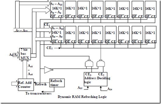
• The following block diagram explains the refreshing logic and 8086 interfacing with dynamic RAM.
• Each chip is of 16K * 1-bit dynamic RAM cell array. The system contains two 16K byte dynamic RAM units. All the address and data lines are assumed to be available from an 8086 microprocessor system.
• The OE pin controls output data buffer of the memory chips. The CE pins are active high chip selects of memory chips. The refresh cycle starts, if the refresh output of the refresh timer goes high, OE and CE also tend to go high.
• The high CE enables the memory chip for refreshing, while high OE prevents the data from appearing on the data bus, as discussed in memory refresh cycle. The 16K * 1-bit dynamic RAM has an internal array of 128*128 cells, requiring 7 bits for row address. The lower order seven lines A0-A6 are multiplexed with the refresh counter output A10-A16.
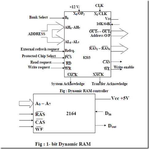
Fig : 1- bit Dynamic RAM
• The pin assignment for 2164 dynamic RAM is as in above fig.
• The RAS and CAS are row and column address strobes and are driven by the dynamic RAM controller outputs. A0 –A7 lines are the row or column address lines, driven by the OUT0 – OUT7 outputs of the controller. The WE pin indicates memory write cycles. The DIN and DOUT pins are data pins for write and read operations respectively.
• In practical circuits, the refreshing logic is integrated inside dynamic RAM controller chips like 8203, 8202, 8207 etc.
• Intel’s 8203 is a dynamic RAM controller that support 16K or 64K dynamic RAM chip. This selection is done using pin 16K/64K. If it is high, the 8203 is configured to control 16K dynamic RAM, else it controls 64K dynamic RAM. The address inputs of 8203 controller accepts address lines A1 to A16 on lines AL0-AL7 and AH0-AH7.
• The A0 lines is used to select the even or odd bank. The RD and WR signals decode whether the cycle is a memory read or memory write cycle and are accepted as inputs to 8203 from the microprocessor.
• The WE signal specifies the memory write cycle and is not output from 8203 that
drives the WE input of dynamic RAM memory chip. The OUT0 – OUT7 set of eight pins is an 8-bit output bus that carries multiplexed row and column addresses are derived from the address lines A1-A16 accepted by the controller on its inputs AL0-AL7 and AH0-AH7.
• An external crystal may be applied between X0 and X1 pins, otherwise with the OP2 pin at +12V, a clock signal may be applied at pin CLK.
• The PCS pin accepts the chip select signal derived by an address decoder. The REFREQ pin is used whenever the memory refresh cycle is to be initiated by an external signal.
• The XACK signal indicates that data is available during a read cycle or it has been written if it is a write cycle. It can be used as a strobe for data latches or as a ready signal to the processor.
• The SACK output signal marks the beginning of a memory access cycle.
• If a memory request is made during a memory refresh cycle, the SACK signal is delayed till the starring of memory read or write cycle.
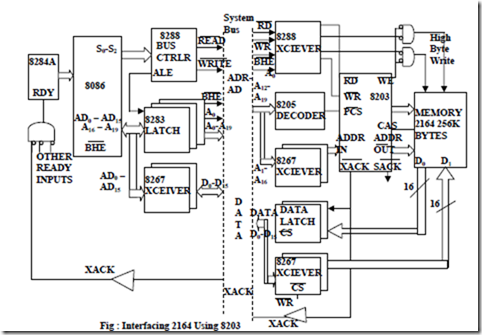
• Following fig shows the 8203 can be used to control a 256K bytes memory subsystem for a maximum mode 8086 microprocessor system.
• This design assumes that data and address busses are inverted and latched, hence the inverting buffers and inverting latches are used (8283-inverting buffer and 8287- inverting latch).
• Most of the functions of 8208 and 8203 are similar but 8208 can be used to refresh the dynamic RAM using DMA approach. The memory system is divided into even and odd banks of 256K bytes each, as required for an 8086 system.
• The inverted AACK output of 8208 latches the A0 and BHE signals required for selecting the banks. If the latched bank select signal and the WE /PCLK output of 8208 both become low. It indicates a write operation to the respective bank.
