Module 1: learning unit 2
8085 Microprocessor
Contents General definitions
• Overview of 8085 microprocessor
• Overview of 8086 microprocessor
• Signals and pins of 8086 microprocessor
The salient features of 8085 µp are:
• It is a 8 bit microprocessor.
• It is manufactured with N-MOS technology.
• It has 16-bit address bus and hence can address up to 216 = 65536 bytes (64KB) memory locations through A0-A15.
• The first 8 lines of address bus and 8 lines of data bus are multiplexed AD0 – AD7.
• Data bus is a group of 8 lines D0 – D7.
• It supports external interrupt request.
• A 16 bit program counter (PC)
• A 16 bit stack pointer (SP)
• Six 8-bit general purpose register arranged in pairs: BC, DE, HL.
• It requires a signal +5V power supply and operates at 3.2 MHZ single phase clock.
• It is enclosed with 40 pins DIP (Dual in line package).
Overview of 8085 microprocessor
8085 Architecture
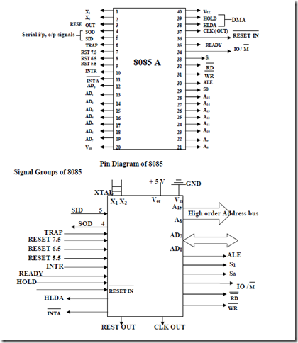
• Pin Diagram
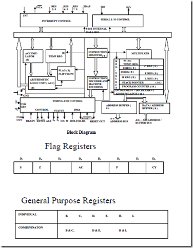
• Functional Block Diagram
Memory
• Program, data and stack memories occupy the same memory space. The total addressable memory size is 64 KB.
• Program memory – program can be located anywhere in memory. Jump, branch and call instructions use 16-bit addresses, i.e. they can be used to jump/branch anywhere within 64 KB. All jump/branch instructions use absolute addressing.
• Data memory – the processor always uses 16-bit addresses so that data can be placed anywhere.
• Stack memory is limited only by the size of memory. Stack grows downward.
• First 64 bytes in a zero memory page should be reserved for vectors used by RST instructions.
• The processor has 5 interrupts. They are presented below in the order of their priority (from lowest to highest):
• INTR is maskable 8080A compatible interrupt. When the interrupt occurs the processor fetches from the bus one instruction, usually one of these instructions:
• One of the 8 RST instructions (RST0 – RST7). The processor saves current program counter into stack and branches to memory location N * 8 (where N is a 3-bit number from 0 to 7 supplied with the RST instruction).
• CALL instruction (3 byte instruction). The processor calls the subroutine, address of which is specified in the second and third bytes of the instruction.
• RST5.5 is a maskable interrupt. When this interrupt is received the processor saves the contents of the PC register into stack and branches to 2CH (hexadecimal) address.
• RST6.5 is a maskable interrupt. When this interrupt is received the processor saves the contents of the PC register into stack and branches to 34H (hexadecimal) address.
• RST7.5 is a maskable interrupt. When this interrupt is received the processor saves the contents of the PC register into stack and branches to 3CH (hexadecimal) address.
• TRAP is a non-maskable interrupt. When this interrupt is received the processor saves the contents of the PC register into stack and branches to 24H (hexadecimal) address.
• All maskable interrupts can be enabled or disabled using EI and DI instructions.
RST 5.5, RST6.5 and RST7.5 interrupts can be enabled or disabled individually using SIM instruction.
• RESET IN: When this signal goes low, the program counter (PC) is set to Zero, µp is reset and resets the interrupt enable and HLDA flip-flops.
• The data and address buses and the control lines are 3-stated during RESET and because of asynchronous nature of RESET, the processor internal registers and flags may be altered by RESET with unpredictable results.
• RESET IN is a Schmitt-triggered input, allowing connection to an R-C network for power-on RESET delay.
• Upon power-up, RESET IN must remain low for at least 10 ms after minimum Vcc has been reached.
• For proper reset operation after the power – up duration, RESET IN should be kept low a minimum of three clock periods.
• The CPU is held in the reset condition as long as RESET IN is applied. Typical Power-on RESET RC values R1 = 75KΩ, C1 = 1µF.
• RESET OUT: This signal indicates that µp is being reset. This signal can be used to reset other devices. The signal is synchronized to the processor clock and lasts an integral number of clock periods.
• SID – Serial Input Data Line: The data on this line is loaded into accumulator bit 7 whenever a RIM instruction is executed.
• SOD – Serial Output Data Line: The SIM instruction loads the value of bit 7 of the accumulator into SOD latch if bit 6 (SOE) of the accumulator is 1.
• HOLD: Indicates that another master is requesting the use of the address and data buses. The CPU, upon receiving the hold request, will relinquish the use of the bus as soon as the completion of the current bus transfer.
• Internal processing can continue. The processor can regain the bus only after the HOLD is removed.
• When the HOLD is acknowledged, the Address, Data RD, WR and IO/M lines are 3-stated.
• HLDA: Hold Acknowledge: Indicates that the CPU has received the HOLD request and that it will relinquish the bus in the next clock cycle.
• HLDA goes low after the Hold request is removed. The CPU takes the bus one half-clock cycle after HLDA goes low.
• READY: This signal Synchronizes the fast CPU and the slow memory, peripherals.
• If READY is high during a read or write cycle, it indicates that the memory or peripheral is ready to send or receive data.
• If READY is low, the CPU will wait an integral number of clock cycle for READY to go high before completing the read or write cycle.
• READY must conform to specified setup and hold times.
• Accumulator or A register is an 8-bit register used for arithmetic, logic, I/O and load/store operations.
• Flag Register has five 1-bit flags.
• Sign – set if the most significant bit of the result is set.
• Zero – set if the result is zero.
• Auxiliary carry – set if there was a carry out from bit 3 to bit 4 of the result.
• Parity – set if the parity (the number of set bits in the result) is even.
• Carry – set if there was a carry during addition, or borrow during subtraction/comparison/rotation.
• 8-bit B and 8-bit C registers can be used as one 16-bit BC register pair. When used as a pair the C register contains low-order byte. Some instructions may use BC register as a data pointer.
• 8-bit D and 8-bit E registers can be used as one 16-bit DE register pair. When used as a pair the E register contains low-order byte. Some instructions may use DE register as a data pointer.
• 8-bit H and 8-bit L registers can be used as one 16-bit HL register pair. When used as a pair the L register contains low-order byte. HL register usually contains a data pointer used to reference memory addresses.
• Stack pointer is a 16 bit register. This register is always decremented/incremented by 2 during push and pop.
• Program counter is a 16-bit register.
• 8085 instruction set consists of the following instructions:
• Data moving instructions.
• Arithmetic – add, subtract, increment and decrement.
• Logic – AND, OR, XOR and rotate.
• Control transfer – conditional, unconditional, call subroutine, return from subroutine and restarts.
• Input/Output instructions.
• Other – setting/clearing flag bits, enabling/disabling interrupts, stack operations, etc.
• Register – references the data in a register or in a register pair.
Register indirect – instruction specifies register pair containing address, where the data is located.
Direct, Immediate – 8 or 16-bit data.

