■ SUMMARY
A microarchitecture consists of a data path and a control section. The data path contains data registers, an ALU, and the connections among them. The control section contains registers for microinstructions (for a microprogramming approach) and for condition codes, and a controller. The controller can be micro- programmed or hardwired. A micro programmed controller interprets microinstructions by executing a micro program that is stored in a control store. A hardwired controller is organized as a collection of flip-flops that maintain state information, and combinational logic that implements transitions among the states.
The hardwired approach is fast, and consumes a small amount of hardware in comparison with the micro programmed approach. The micro programmed approach is flexible, and simplifies the process of modifying the instruction set. The control store consumes a significant amount of hardware, which can be reduced to a degree through the use of nanoprogramming. Nanoprogramming adds delay to the microinstruction execution time. The choice of micro programmed or hard- wired control thus involves trade-offs: the micro programmed approach is large and slow, but is flexible and lends itself to simple implementations, whereas the hardwired approach is small and fast, but is difficult to modify, and typically results in more complicated implementations.
■ FURTHER READING
(Wilkes, 1958) is a classic reference on microprogramming. (Mudge, 1978) cov- ers microprogramming on the DEC PDP 11/60. (Tanenbaum, 1990) and (Mano, 1991) provide instructional examples of micro programmed architec- tures. (Hill and Peterson, 1987) gives a tutorial treatment of the AHPL hardware description language, and hardwired control in general. (Lipsett et. al., 1989) and (Navabi, 1993) describe the commercial VHDL hardware description language and provide examples of its use. (Gajski, 1988) covers various aspects of silicon compilation.
Gajski, D., Silicon Compilation, Addison Wesley, (1988).
Hill, F. J. and G. R. Peterson, Digital Systems: Hardware Organization and Design, 3/e, John Wiley & Sons, (1987).
Lipsett, R., C. Schaefer, and C. Ussery, VHDL: Hardware Description and Design, Kluwer Academic Publishers, (1989).
Mano, M., Digital Design, 2/e, Prentice Hall, (1991).
Mudge, J. Craig, Design Decisions for the PDP11/60 Mid-Range Minicomputer, in Computer Engineering, A DEC View of Hardware Systems Design, Digital Press, Bedford MA, (1978).
Navabi, Z., VHDL: Analysis and Modeling of Digital Systems, McGraw Hill, (1993).
Tanenbaum, A., Structured Computer Organization, 3/e, Prentice Hall, Engle- wood Cliffs, New Jersey, (1990).
Wilkes, M. V., W. Redwick, and D. Wheeler, “The Design of a Control Unit of an Electronic Digital Computer,” Proc. IRE, vol. 105, p. 21, (1958).
■ PROBLEMS
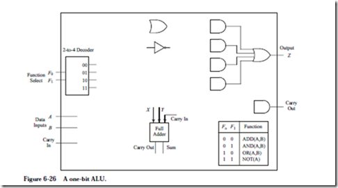
6.1 Design a 1-bit arithmetic logic unit (ALU) using the circuit shown in Figure 6-26 that performs bitwise addition, AND, OR, and NOT on the 1-bit inputs A and B. A 1-bit output Z is produced for each operation, and a carry is also produced for the case of addition. The carry is zero for AND, OR, and
NOT. Design the 1-bit ALU using the components shown in the diagram. Just draw the connections among the components. Do not add any logic gates, MUXes, or anything else. Note: The Full Adder takes two one-bit inputs (X and Y) and a Carry In, and produces a Sum and a Carry Out.
6.2 Design an ALU that takes two 8-bit operands X and Y and produces an 8-bit output Z. There is also a two-bit control input C in which 00 selects log- ical AND, 01 selects OR, 10 selects NOR, and 11 selects XOR. In designing your ALU, follow this procedure: (1) draw a block diagram of eight 1-bit ALUs that each accept a single bit from X and Y and both control bits, and produce the corresponding single-bit output for Z; (2) create a truth table that describes a 1-bit ALU; (3) design one of the 1-bit ALUs using an 8-to-1 MUX.
6.3 Design a control unit for a simple hand-held video game in which a character on the display catches objects. Treat this as an FSM problem, in which you only show the state transition diagram. Do not show a circuit. The input to the control unit is a two-bit vector in which 00 means “Move Left,” 01 means “Move Right,” 10 means “Do Not Move,” and 11 means “Halt.” The output Z is 11 if the machine is halted, and is 00, 01, or 10 otherwise, corresponding to the input patterns. Once the machine is halted, it must remain in the halted state indefinitely.
6.4 In Figure 6-3, there is no line from the output of the C Decoder to %r0.
Why is this the case?
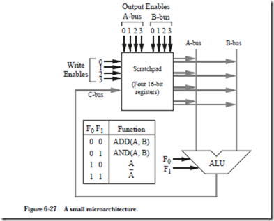
6.5 Refer to diagram Figure 6-27. Registers 0, 1, and 2 are general purpose
registers. Register 3 is initialized to the value +1, which can be changed by the microcode, but you must make certain that it does not get changed.
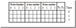
a) Write a control sequence that forms the two’s complement difference of the contents of registers 0 and 1, leaving the result in register 0. Symbolically, this might be written as: r0 ¬ r0 – r1. Do not change any registers except r0 and r1 (if needed). Fill in the table shown below with 0’s or 1’s (use 0’s when the choice of 0 or 1 does not matter) as appropriate. Assume that when no registers are selected for the A-bus or the B-bus, that the bus takes on a value of 0.
b) Write a control sequence that forms the exclusive-OR of the contents of registers 0 and 1, leaving the result in register 0. Symbolically, this might be written as: r0 ¬ XOR(r0, r1). Use the same style of solution as for part (a).
6.6 Write the binary form for the microinstructions shown below. Use the style shown in Figure 6-17. Use the value 0 for any fields that are not needed.
6.7 Three binary words are shown below, each of which can be interpreted as a microinstruction. Write the mnemonic version of the binary words using the micro-assembly language introduced in this chapter.
6.8 Rewrite the microcode for the call instruction starting at line 1280 so that only 3 lines of microcode are used instead of 4. Use the LSHIFT2 operation once instead of using ADD twice.
6.9 (a) How many microinstructions are executed in interpreting the subcc instruction that was introduced in the first Example section? Write the numbers of the microinstructions in the order they are executed, starting with microinstruction 0.
(b) Using the hardwired approach for the ARC microcontroller, how many states are visited in interpreting the addcc instruction? Write the states in the order they are executed, starting with state 0.
6.10 (a) List the microinstructions that are executed in interpreting the ba instruction.
(b) List the states (Figure 6-22) that are visited in interpreting the ba instruction.
6.11 Register %r0 can be designed using only tri-state buffers. Show this design.
6.12 What bit pattern should be placed in the C field of a microword if none of the registers are to be changed?
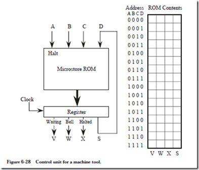
6.13 A control unit for a machine tool is shown in Figure 6-28. You are to cre-
ate the microcode for this machine. The behavior of the machine is as follows: If the Halt input A is ever set to 1, then the output of the machine stays halted forever and outputs a perpetual 1 on the X line, and 0 on the V and W lines. A waiting light (output V) is enabled (set to 1) when no inputs are enabled. That is, V is lit when the A, B, and C inputs are 0, and the machine is not halted. A bell is sounded (W=1) on every input event (B=1 and/or C=1) except when the machine is halted. Input D and output S can be used for state information for your microcode. Use 0’s for any fields that do not matter. Hint: Fill in the lower half of the table first.
6.14 For this problem, you are to extend the ARC instruction set to include a new instruction by modifying the microprogram. The new ARC instruction to be microcoded is:
xorcc — Perform an exclusive OR on the operands, and set the condition codes accordingly. This is an Arithmetic format instruction. The op3 field is 010011.
Show the new microinstructions that will be added for xorcc.
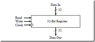
6.15 Show a design for a four-word register stack, using 32-bit registers of the form shown below:
Four registers are stacked so that the output of the top register is the input to the second register, which outputs to the input of the third, which outputs to the input of the fourth. The input to the stack goes into the top register, and the output of the stack is taken from the output of the top register (not the bottom register). There are two additional control lines, push and pop, which cause data to be pushed onto the stack or popped off the stack, respectively, when the corresponding line is 1. If neither line is 1, or if both lines are 1, then the stack is unchanged.
6.16 In line 1792 of the ARC microprogram, the conditional GOTO appears at the end of the line, but in line 8 it appears at the beginning. Does the position of the GOTO within a micro-assembly line matter?
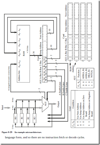
6.17 A microarchitecture is shown in Figure 6-29. The datapath has four registers and an ALU. The control section is a finite state machine, in which there is a RAM and a register. For this microarchitecture, a compiler translates a high level program directly into microcode; there is no intermediate assembly
For this problem, you are to write the microcode that implements the instructions listed below. The microcode should be stored in locations 0, 1, 2, and 3 of the RAM. Although there are no lines that show it, assume that the n and z bits are both 0 when C0C1 = 00. That is, A23 and A22 are both 0 when there is no possible jump. Note: Each bit of the A, B, and C fields corresponds directly to a register. Thus, the pattern 1000 selects register R3, not register 8, which does not exist. There are some complexities with respect to how branches are made in this microarchitecture, but you do not need to be concerned with how this is done in order to generate the microcode.
6.18 In line 2047 of the ARC microprogram shown in Figure 6-15, would the program behave differently if the “GOTO 0” portion of the instruction is deleted?
6.19 In horizontal microprogramming, the microwords are wide, whereas in vertical microprogramming the words are narrow. In general, horizontal microwords can be executed quickly, but require more space than vertical microwords, which take more time to execute. If we make the microword for- mat shown in Figure 6-11 more horizontal by expanding the A, B, and C fields to contain a single bit for each of the 38 registers instead of a coded six-bit version, then we can eliminate the A, B, and C decoders shown in Figure 6-3. This allows the clock frequency to be increased, but also increases the space for the microstore.
(a) How wide will the new horizontal microword be?
(b) By what percentage will the microstore increase in size?
6.20 Refer to Figure 6-7. Show the ALU LUT0 and ALU LUTx (x > 0) entries for the INC(A) operation.
6.21 On some architectures, there is special hardware that updates the PC, which takes into account the fact that the rightmost two bits are always 0. There is no special hardware presented in this chapter for updating the PC,
and the branch microcode in lines 2 – 20 of Figure 6-15 has an error in how the PC is updated on line 12 because branch displacements are given in terms of words. Identify the error, and explain how to fix it.
